Note: Descriptions are shown in the official language in which they were submitted.
CA 02211028 1997-08-04
PROCESS AND APPARATUS FOR MANUFACTURING POLYCRYSTALLINE
SILICON, AND PROCESS FOR MANUFACTURING SILICON WAFER FOR SOLAR
CELL
BACKGROUND OF THE INVENTION
1. Field of the Invention
This invention relates to a process and apparatus for
manufacturing polycrystalline silicon and a process for
manufacturing a silicon wafer for a solar cell. In
particular, this invention pertains to a technique which
employs metallic silicon or silicon oxide as a starting
material and permits the continuous flow production from
polycrystalline silicon to an end product, that is, a
polycrystalline silicon wafer for a solar cell.
2. Description of the Related Art
Studies on solar cells have been made for many years.
Recently, those having a photoelectric transfer efficiency of
even about 13 to 15% under sun light on the ground have
appeared and they are now being industrialized for various
applications. In our country, however, solar cells are not
so popular as an energy source for domestic electric power,
automobiles, ships or machine tools, because a technique to
mass-produce a silicon wafer at a low cost, which is
necessary for the manufacture of solar cells, has not yet
been established.
At present, for the manufacture of a silicon wafer
1
CA 02211028 1997-08-04
for a solar cell, a high-purity silicon, which is in the mass
form and conforms to the specification of a semiconductor, is
once manufactured through a chemical process by using as a
starting material a low purity metallic silicon (99.5 wt.%
Si). Then, high-purity silicon in the mass form is re-melted
and is adjusted to have a chemical composition suited to a
solar cell by a metallurgical process. The resulting
molten silicon is formed into an ingot by the pulling method
or directional solidification method, followed by slicing
into thin plates. Described specifically, as shown in
FIG S, metallic silicon is first reacted with hydrochloric
acid and formed into a trichlorosilane gas. After the gas so
obtained is fractionated to remove the impurity elements, the
residue is reacted with a hydrogen gas, whereby high-purity
silicon is precipitated from the gas by the so-called CVD
(Chemical Vapor Deposition) method. The high-purity silicon
therefore becomes only an aggregate of silicon grains owing
to the weak bonding power between crystal grains. The boron
contained in the high-purity silicon forming the aggregate is
reduced even in the order of O.OOI ppm and does not reach
the concentration necessary for satisfying the specific
resistivity of 0.5 to I.5 ohm~cm which is the specification
for P-type semiconductor wafer. In order to use the above
high-purity silicon for a solar cell, it is indispensable to
adjust the specific resistivity and to control the
crystallinity of single crystals or crystal grains so as to
2
. CA 02211028 1997-08-04
have a particle size not smaller than several mm and have a
grain boundary so as not to exert adverse effects on the
photoelectric transfer efficiency. The above silicon cannot
be formed into a wafer without further treatment. As shown in
the right hand of FIG. 5, it becomes necessary to form a
wafer after re-melting the high-purity silicon mass,
adjusting the components of the melt (by the addition of
boron) and forming into an ingot (pulling method for single
crystals, while directional solidification for polycrystals).
The above-described manufacturing method is however
accompanied with the drawbacks that it requires much labor to
re-adjust (mainly, by the addition of boron) the components
of a silicon ingot, which has a purity intentionally
heightened to be suitable for semiconductor, to be suitable
for solar cells or to purify the ingot; its yield is
inferior; it additionally requires equipment and energy for
re-melting; and therefore it costs high. As described above,
the solar cells available now are therefore expensive, which
prevents them from being popularly used. The purity
heightening of metallic silicon by a chemical process is
also accompanied with the generation of a large amount of
pollutants such as silane and chloride, which prevents mass-
production. According to the technique recently disclosed,
the manufacturing process tends to be studied, divided into
steps such as purity increase of metallic silicon or
solidification technique, which is presumed to be influenced
3
CA 02211028 1997-08-04
by the above-described manufacturing method.
For example, Japanese Published Unexamined Patent
Application No. HEI 5-139713 discloses a process in which
silicon having a Iow boron content is obtained by maintaining
molten silicon in a container composed of silica or composed
mainly of silica, and injecting a plasma gas jet flow of an
inert gas to the surface of the molten silicon, while blowing
an inert gas upwardly from the bottom of the container.
Japanese Published Unexamined Patent Application No.
HEI 7-17704 discloses a process permitting the efficient
removal of boron by forming I.5 to I5 kg of Si02 per kg
silicon in advance on the surface of metallic silicon powders
upon melting metallic Silicon through an electron beam.
Concerning solidification technique, Japanese Published
Unexamined Patent Application No. SHO 61-141612 proposes a
technique to prevent, upon casting molten silicon into a
mold, precipitation of inclusion in a silicon ingot by
turning the mold. In addition, the present applicants
themselves are now proposing a method for purifying molten
metallic silicon by directional solidification in Japanese
Patent Application HEI 7-29500 (filed on February 17, 1995).
It is impossible to say that there does not exist a
technique to manufacture solar cell silicon directly from
metallic silicon. For example, Japanese Published
Unexamined Patent Application No. SHO 62-252393 discloses a
process in which a starting material silicon, which is once
4
CA 02211028 1997-08-04
used as a semiconductor but disposed as an electron industry
waste, is subjected to zone melting by plasma jet generated
by a mixed gas of argon, hydrogen and oxygen. This process
aims principally at the use of an industrial waste so that it
does not become a mainly-employed technique suited for mass
production of a silicon wafer. In addition, although silicon
is used as a raw material, its purity has been once increased
so that the process is only a variation of the
above-described cumbersome manufacturing process. Japanese
Published Unexamined Patent Application No. SHO 63-218506
discloses a process for manufacturing, by plasma melting,
silicon in the mass form for solar cells or electronics from
metallic silicon in the farm of powders, granules or
polished dusts. This method is based on the principle of the
zone melting method using the same plasma as that disclosed
in the above Japanese Published Unexamined Patent
Application No. SHO 62-252393 and is accompanied with the
drawback that mass production cannot be carried out in spite
of large electricity consumption. According to Examples of
the above official gazette, only a silicon rod of 50 g or so
is obtained on a laboratory scale and it does not include a
description of increasing the size of the silicon wafer for a
solar cell to a practical size.
SUMMARY OF THE INVENTION
CA 02211028 1997-08-04
With the forgoing in view, an object of the present
invention is to provide a process and apparatus for
mass-producing, at a low cost in continuous flow production,
polycrystalline silicon by using metallic silicon or silicon
oxide as a starting raw material, and a wafer manufactured
using it.
With a view to attaining the above object, the
inventors of the present invention have carried out an
extensive investigation, paying attention to obtaining the
maximum economic effects without using a chemical process
but only a metallurgical process, leading to the completion
of the present invention.
In a first aspect of the present invention, there is
thus provided a process for manufacturing polycrystalline
silicon from metallic silicon, which comprises the following
steps:
A: melting metallic silicon under vacuum to remove the
phosphorus contained therein by evaporation, and then
carrying out solidification of the residue for the removal
of the impurity elements from the molten silicon (which may
hereinafter be called "melt"), thereby obtaining a first
ingot;
B: removing the impurity concentrated portion of the
first ingot by cutting;
C: re-melting the remaining portion, removing boron and
carbon from the melt by oxidizing under an oxidizing
6
CA 02211028 1997-08-04
atmosphere, and in succession, blowing an argon gas or a
mixed gas of argon and hydrogen into the melt for
deoxidization.
D: casting the deoxidized melt in a mold, followed by
directional solidification to obtain a second ingot; and
E: removing the impurity concentrated portion of the
second ingot by cutting.
In a further aspect of the present invention, there is
also provided a process for the preparation of
polycrystalline silicon, wherein in the above-described
process, said metallic silicon is obtained by reductive
smelting of silicon oxide.
In a still further aspect of the present invention,
there is also provided a process for the preparation of
polycrystalline silicon, which comprises transferring said
metallic silicon under molten state, which has been obtained
by smelting of silicon oxide in the above-described process,
into a crucible, removing boron and carbon from it
by oxidizing under an oxidizing atmosphere, and carrying out
solidification, followed by the above-described step B,
melting under vacuum and the above-described steps C, D and
E.
In a still further aspect of the present invention,
there is also provided a process for the preparation of
polycrystalline silicon, which comprises forming the
z
above-described oxidizing atmosphere from an HZO, COZ or Oz
7
CA 02211028 1997-08-04
gas in an amount small enough so that the whole interface
between the melt and the gas will not be covered with
silicon oxide, removing silicon oxide formed on the surface
of the melt by locally heating by plasma arc, or blowing an
H20, COz or Oz gas into the melt instead of placing the melt
under the above-described oxidizing atmosphere.
In a still further aspect of the present invention,
there is also provided a process for the preparation of
polycrystalline silicon, which comprises using Si02 or Si3N4
as a mold releasing agent, setting a solidification interface
moving rate at 5 mm/min or less, said solidification being
carried out for the removal of impurities, setting a
solidification interface moving rate at 2 mm/min or less for
directional solidification, or cutting the ingot at a height
at least 70o above the bottom of the ingot.
In a still further aspect of the present invention,
there is also provided a process for the preparation of
polycrystalline silicon which comprises setting a phosphorus
concentration of the melt at 0.3 ppm or less and a boron
concentration at 0.6 ppm or less or a carbon concentration
at 10 ppm or less.
The present invention also relates to an apparatus for
manufacturing polycrystalline silicon. In a still further
aspect of the present invention, there is also provided an
apparatus for manufacturing polycrystalline silicon, which
comprises heating means for melting or heating metallic
8
CA 02211028 2001-03-12
silicon, a retaining container for retaining molten
metallic silicon, a first mold in which the melt is cast
from the retaining container, a vacuum chamber for removing
phosphorus by evaporation, said chamber surrounding the
retaining container arid the f first mold, means for removing
an impurity concentrated portion of an ingot from the first
mold, re-melting mean~o for re-melting or heating a portion
of said ingot from the first mold containing fewer
impurities, a smelting container for retaining the re-melt
11) a nozzle for blowing or spraying an oxidizing gas, hydrogen
gas or a mixed gas of hydrogen and argon to the re-melt in
the smelting container and a second. mold for forming the
deoxidized re-melt into a cast ingot.
In a still further aspect of the present invention,
there is also provided an apparatus for manufacturing
polycrystalline silicon, wherein the degree of vacuum :in the
above-described vacuum chamber is set at 10-3 torr or higher,
the retaining container is a water-cooling
jacket made of copper o:r a graphite crucible; and the
2(t smelting container is a crucible made of SiOZ, an SiOz
stamped crucible or an Si02 lined crucible.
In a still further aspect of the present invention,
there is also provided an apparatus for manufacturing
polycrystalline, wherein the above-described heating mE:ans
is an electron gun; or the above-described re-melting means
is a plasma torch or a DC arc source.
In a still further aspect of the present invention,
there is also provided an apparatus for the preparation of
9
CA 02211028 1997-08-04
polycrystalline silicon, wherein the above-described first
and second molds have side walls formed of a heat insulating
material and have a bottom formed of a water cooling jacket;
and a heating source for heating the cast melt is disposed
above the molds; or a W/H ratio, that is, the ratio of the
diameter W to the height H of said mold is set at greater
than 0.5.
In a still further and essential aspect of the present
invention, there is thus provided a process for the
manufacture of a silicon wafer for a solar cell, which
comprises slicing an ingot of polycrystalline silicon, which
has been obtained by any one of the above-described
processes, to a thickness of 100 to 450 a m.
According to the present invention, polycrystalline
silicon or a silicon wafer for a solar cell is manufactured
by any one of the above-described methods or apparatuses so
that the component adjustment of high-purity silicon, which
is indispensable in the conventional method, is not
required. The present invention also makes it possible to
reduce the unnecessary consumption of energy. Since not a
chemical process which is characterized by the generation of
a large amount of pollutants but only a metallurgical process
is adopted, the present invention makes it possible to
enlarge the production equipment. As a result, a silicon
wafer for a solar cell having excellent photoelectric
transfer efficiency can be provided at a cost by far lower
t
s
t
1 0
3
CA 02211028 1997-08-04
than the conventional one. Furthermore, polycrystalline
silicon obtained by the enforcement of the present invention
can be used effectively not only for the manufacture of a
wafer but also for the use as a raw material for iron
manufacture or the like.
As described above, the present invention makes it
possible to avoid the consumption of unnecessary energy and
enlarge the manufacturing equipment, thereby mass-producing
polycrystalline silicon or polysilicon wafer for a solar cell
having relatively good purity. As a result, a
polycrystalline silicon wafer for a solar cell which has a
photoelectric transfer efficiency on the ground on the same
level with that obtained in the conventional method can be
obtained at a markedly low cost, from which the wide
diffusion of solar cells are much expected. Polycrystalline
silicon can be used effectively as a raw material for iron
manufacture as well as that for a wafer.
According to the present invention, high-purity
polycrystalline silicon and a silicon wafer for a solar cell
can be manufactured through a continuous flow production
based on only a metallurgical process. Accordingly, the
equipment can be enlarged freely and unnecessary energy can
be omitted. The present invention is therefore very useful
for the manufacture of a silicon wafer for a solar cell.
1 1
CA 02211028 1997-08-04
BRIEF DESCRIPTION OF THE DRAWINGS
FIG. 1 is a flow chart illustrating one embodiment of a
manufacturing process of polycrystalline silicon and a silicon
wafer for a solar cell according to the present
invention;
FIG. 2 is a flow chart illustrating another embodiment
of the manufacturing process of polycrystalline silicon and a
silicon wafer for a solar cell according to the present
invention;
FIG. 3 is a schematic view illustrating an apparatus
embodying the manufacturing process of polycrystalline
silicon and a silicon wafer for a solar cell according to the
present invention;
FIG. 4 illustrates another apparatus embodying the
manufacturing process of polycrystalline silicon and a
silicon wafer for a solar cell according to the present
invention; and
FIG. 5 is a flow chart illustrating the conventional
process for manufacturing a silicon wafer for a solar cell.
DETAILED DESCRIPTION OF THE PREFERRED EMBODIMENTS
In FIG. 1, one embodiment of the manufacturing process
of polycrystalline silicon and a silicon wafer for a solar
cell according to the present invention is shown together in
one flow chart (manufacture of the wafer is shown, enclosed
with a dotted line).
1 2
CA 02211028 1997-08-04
First, metallic silicon having a relatively low purity
(99.5 wt.o Si) is charged in a retaining container made of
graphite or a water-cooling retaining container made of
copper and then melted under vacuum. At this time, heating
may be conducted making use of the methods known to date
such as gas heating or electric heating, with heating by an
electron gun being most preferred. Here, the metallic
silicon so melted is maintained for a predetermined time
(for example, 30 to 60 minutes) in the above retaining
container at a temperature not lower than 1450° C but not
higher than 1900° C, whereby phosphorus and aluminum, among
impurity elements contained in the melt, are removed by
evaporation (vacuum smelting). It is preferred that the
phosphorus concentration in the melt is 0.3 ppm or less.
Then, in order to remove the impurity elements such as Fe,
Al, Ti and Ca to be 100 ppm or less, the melt is cast into a
first cast and is cooled upwardly from the bottom so that the
moving rate of solidification interface will be 5 mm/min. As
a result, an ingot in which the melt having concentrated
impurity elements has been solidified last is obtained.
In succession, the upper 30% portion of the ingot
having the concentrated impurity elements therein is removed
by cutting. The remaining portion of the ingot is charged
in a melt furnace equipped with, for example, a plasma arc,
whereby the ingot is re-melted. Also in this case, the
heating means is not limited to the plasma arc. The
1 3
CA 02211028 1997-08-04
melt is heated to a temperature not lower than 1450 ° C and
at the same time is reacted with an oxidizing gas atmosphere,
whereby boron and carbon are removed from the melt as oxides
(oxidative smelting). After oxidative smelting, an argon gas
or a mixed gas of argon and hydrogen is blown into the melt
for a predetermined time. As a result, oxygen in the melt is
deoxidized to the level not higher than 10 ppm. Incidentally,
the above-described oxidative smelting may be carried
out either in a vacuum chamber or in the air. The deoxidized
melt is then cast into a second mold coated with a mold
releasing agent, followed by directional solidification,
whereby a final ingot is obtained. Impurity elements exist
in the concentrated form in the upper portion of the ingot so
that the portion (generally, 20% or so) is removed by cutting
and the remaining portion is provided as a product of
polycrystalline silicon.
Polycrystalline silicon is prepared as described above.
It is only necessary to slice the above-described remaining
portion by a multi-wire saw into thin plates of 100 to 450
~ m thickness.
Metallic silicon, which is a starting material, is
generally available by reductive smelting of silicon oxide
so that the use of silicon oxide as a starting material is
also added to the present invention. Any known methods can
be employed to smelt silicon oxide into that having a purity
on the same level with that of the metallic silicon used in
1 4
CA 02211028 1997-08-04
the first step of the present invention. For example, silicon
oxide is melted and reduced by using a carboneous material as
a reducing agent. In the present invention, considered is a
method of removing the components, which are not necessary
for polycrystalline silicon or a silicon wafer for a solar
cell, in advance upon obtaining metallic silicon from silicon
oxide. It is a method as shown in the flow chart of FIG. 2,
wherein metallic silicon which has been obtained from silicon
oxide, has a relatively low purity and is under molten state
is charged in a smelting container (for example, crucible)
and so-called preliminary smelting is effected. Described
specifically, an oxidizing gas (H20, COz or the like) is
blown into the melt in the crucible, boron and carbon are
removed as oxides and then, the residue is solidified. The
ingot so obtained is melted in the above-described vacuum
chamber, phosphorus is removed from the melt by vacuum
smelting and the residue is subjected to directional
solidification, whereby an ingot of polycrystalline silicon
is obtained. It is only necessary to slice the ingot into
thin plates as described above to obtain a wafer. This
process has a merit in that the above-described steps of
"boron and carbon removal" and "solidification for the
removal of impurities" of the present invention can be
omitted by changing a part of ordinary metallic silicon
preparation operations. As a result, this process makes it
possible to omit some of the apparatuses and brings about
1 5
' CA 02211028 1997-08-04
effects for reducing energy consumption, whereby
polycrystalline silicon and a silicon wafer for a solar cell
on the same level with those obtained by the
above-described process of the present invention are
available at a lower cost. In particular, if boron and carbon
removal is conducted by those who prepare metallic silicon,
operations subsequent to it can be carried out more easily by
the manufacturer of polycrystalline silicon or wafer.
Incidentally, the reason for setting the moving rate of
the solidification interface at 5 mm/min or lower in the case
of the first mold and at 2 mm/min in the case of the second
mold is because moving rates higher than the above disturb
sufficient concentration of impurity metal elements in the
upper part of the ingot. The reason for cutting the ingot at
a height not lower than 70% from the bottom of the ingot is
because the target composition as polycrystalline silicon
can be attained at the remaining lower portion. In the
present invention, the degree of vacuum in the vacuum chamber
is set at 10-3 torr or higher because it is suited for
phosphorus removal by evaporation judging from the vapor
pressure of phosphorus in metallic silicon.
In the present invention, the phosphorus concentration
of the melt is set at 0.3 ppm or lower in order to secure
stable operation of solar cells, while the boron
concentration of the melt is set at 0.6 ppm or lower in order
to obtain polycrystalline silicon suited for a P-type
1 6
CA 02211028 1997-08-04
semiconductor wafer. The carbon concentration set at 10
ppm or lower makes it possible to suppress the precipitation
of SiC in silicon crystals, thereby preventing the lowering
in the photoelectric transfer efficiency.
Furthermore, in the present invention, a copper-made
water-cooling jacket or a graphite crucible is employed as
the above-described retaining container upon melting of
metallic silicon and an Si02 crucible or Si02 stamped or
lined crucible is used as the above-described smelting
container, because silicon tends to react with other
substances and when a crucible made of another substance is
used, component elements of the substance is mixed in
silicon. Incidentally, when boron is removed upon preparation
of metallic silicon, inexpensive A1203, MgO, graphite or the
like can be employed for the lining of the refractory,
because if impurities are mixed in, they can be removed at
the subsequent step. The mold releasing agent of the mold
used for solidification is specified to SiOz or Si3N4 because
of the same reason. Since the molten silicon expands by 10%
in volume when solidified, the mold releasing agent is
necessary for preventing the stress from remaining on the
ingot.
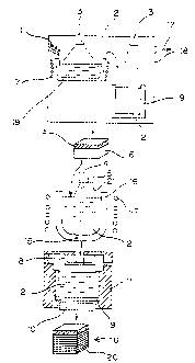
In addition, an apparatus according to the present
invention is constructed so that as shown in FIG. 3, the melt
2 of metallic silicon 1 flows to the subsequent stage almost
continuously except at the time of solidification. This
1 7
CA 02211028 1997-08-04
structure makes it possible to carry out preparation smoothly
and to shorten the operation time, leading to the reduction
in the manufacturing cost. Besides, since the apparatuses
used in the present invention are operated based on only the
metallurgical process, they can be enlarged considerably and
are free from generation of pollutants. Cost reduction by
mass production can also be expected.
The oxidizing atmosphere for the removal of boron and
carbon from the melt 2 is not required to have high acidifying
power. Preferred as the oxidizing gas is H20 or CO2. When
acidifying power is high, an Si02 film is formed on the
surface of the melt, which hinders the removal of boron and
COZ. In such a case, injection of arc from a plasma torch 4
or DC arc source is necessary for the removal of such a
film. The above-described oxidizing gas may be blown
directly into the melt. The material of a nozzle 5 from
which the oxidizing gas is blown is limited to graphite or
SiOz, because other materials contaminate the melt 2.
Incidentally, as a cutting machine (not illustrated)
for cutting the ingot 6 released from the second mold 9 into
thin plates, a known multi-wire saw or multi-blade saw can be
used without problems. The reason why the thickness of the
thin plate is set at 100 to 450 ~c m is because the plate is too
weak at the thickness less than 100 ~c m, while it has lowered
photoelectric transfer efficiency at the thickness exceeding
450 ~ m.
a
1 8
CA 02211028 1997-08-04
In the apparatus according to the present invention, a
particular consideration is taken for the structure of the
mold 9 in which solidification is carried out. Described
specifically, as shown in FIG. 3, the mold is shaped into a
so-called washball having a diameter W . height H ratio of
0.5 or greater. In addition, it is constructed to have a
heat insulating material 11 as a side wall, a water-cooled
jacket 10 as a bottom and a heating source 8 disposed in the
upper part of the mold so that the moving rate of the
solidification interface can be regulated.
In the present invention, it is also possible to carry
out the solidification operations (solidification - re-
melting) in the first mold and second mold in repetition.
Alternatively, after a plurality of molds are provided and
the above-described retaining container or smelting container
is enlarged, the melt may be poured from the enlarged
container in portions to the plural molds. Moreover, it is
not necessary to effect the steps A, B, C, D and E in this
order except that the steps D and E come last.
(Example 1)
As shown in FIG. 3, an electron gun 3 of 300 KW in output
was installed on the upper part of a vacuum chamber 18.
Metallic silicon 1 was fed to a retaining container 19
(which is also called a melting furnace) made of graphite at
kg/hour and was melted. At this time, the degree of
vacuum in the vacuum chamber 18 was 10-5 torr. From the
1 9
CA 02211028 1997-08-04
melt 2, a portion of phosphorus and aluminum elements were
evaporated and removed. The remaining melt 2 was then cast
into a water-cooling type copper-made mold 9. While the
surface of the melt was exposed to electron beam 3 to
maintain the molten state, the melt was solidified from the
bottom at a solidification interface moving rate of 1 mm/min,
whereby 50 kg of an ingot 6 were obtained. The upper 20%
portion of the ingot 6 (the portion A) was removed by cutting
to obtain an ingot having a chemical composition as shown in
Table 1.
Table 1
( Unit:ppm )
B P Fe A1 Ti La C O
Metallic 7 23 980 860 180 950 ~-5000 -
silicon
Ingot after
crude 7 <0.1 10 8.5 2 10 35 -
purification
Wafer 0.1 <0.1 <0.1 <0.1 <0.1 <0.1 3.5 5.7
2 0
CA 02211028 1997-08-04
The remaining portion of the ingot 6 was then melted
in a silica crucible (smelting container) I6 above which a
plasma torch 4 of 100 KW in output was disposed. The melt was
kept at a temperature of 1600 ° C and a mixed gas 2I of argon
and water vapor, said gas containing 15 vol.~ of water vapor,
was sprayed to the surface of the melt. At this time, a
sample was taken from the melt Z and its specific resistivity
was measured. About two hours later, the specific
resistivity became I ohm~ cm so that the mixed gas 21 was
changed to an argon gas and deoxidization was effected for 30
minutes. The melt was then poured into a second mold which
was made of graphite and coated with Si3NQ as a mold release
agent and was solidified by cooling upwardly from the bottom
under an argon gas atmosphere, whereby an ingot was
obtained. At this time, a graphite heater $ was disposed in
the upper part of the mold 9 by which the surface of the melt
was heated. As a result, the moving rate of the
solidification interface was 0.7 mm/min.
After the completion of the solidification, the upper
30% of the ingot 6 so obtained was removed by cutting and the
remaining portion of the ingot was provided as a product of
polycrystalline silicon. The product so obtained was sliced
into thin plates having a thickness of 350 ~ m, by a
mufti-wire saw, whereby 300 silicon wafers for solar cells,
each wafer having a size of 15 cm x I5 cm, were
manufactured. These wafers each had a specific resistivity
2 1
CA 02211028 1997-08-04
of 1.2 ohm~cm, had a minority carrier whose life time was 12
sec and, had a photoelectric transfer efficiency of 13.8%.
Its chemical composition is as shown in Table 1.
(Example 2)
In a similar manner to Example 1, an ingot 6 was
obtained from the first mold. The upper 70% portion of the
ingot was melted in a silica crucible (smelting container) 16
above which a plasma torch 4 of 100 KW in output was
disposed. Into the melt 2 maintained at 1600 ° C, a mixed
gas 21 of argon and water vapor, said gas containing 15 vol.o
of water vapor, was blown at a rate of 10 liter/min through a
porous plug 15 disposed at the bottom of the crucible 16,
whereby boron and carbon were removed from the melt. The
residue was subjected to deoxidization, directional
solidification and removal by cutting, whereby a product of
polycrystalline silicon was obtained. The product was sliced
in a similar manner to Example 1, whereby silicon wafers
for solar cells were manufactured.
The size, number and performance of the wafer so
obtained were much the same with those of the wafer obtained
in Example 1.
(Example 3)
Using silicon oxide as a starting material, an arc
electric furnace 12 as shown in FIG. 4 and a carbonaceous
reducing agent, melting and reduction were carried out,
whereby molten metallic silicon having a chemical composition
CA 02211028 1997-08-04
as shown in Table 2 was manufacture. In a crucible 14
equipped with a porous plug 15 at the bottom thereof and
lined with a siliceous refractory, 50 kg of the metallic
silicon 1 were charged. Then, a mixed gas of argon and
water vapor, said gas containing 20 vol% of water vapor,
was blown into the melt for 30 minutes through the porous
plug 15. The remaining melt 2 was heated to 1650 ° C by
the oxidizing heat of silicon and boron- and carbon-
removal reaction occurred. The melt 2 was cast into a first
mold which had an SiC-made heater disposed in the upper part
of the mold and had a bottom cooling system, and was
solidified by cooling at a moving rate of the solidification
surface at 1.5 mm/min. The lower 80o portion of the ingot so
obtained was melted in succession in the retaining container
disposed in the above-described vacuum chamber, followed by
dephosphorization and deoxidization. The resulting melt
was poured into the second mold, whereby directional
solidification was effected. The upper 30o portion of the
ingot 6 so obtained was removed by cutting and the remaining
portion was provided as a product of polycrystalline
silicon. The product was sliced by a multi-blade saw into
thin plates of the above size, whereby 300 polycrystalline
silicon wafers for solar cells were obtained. The wafers
each had a specific resistivity of 0.9 ohm cm, had a
minority carrier whose life time was 10 ~ sec and had a
photoelectric transfer efficiency of 13.5%. It had a
2 3
CA 02211028 1997-08-04
chemical composition as shown in Table 2.
Table 2 ( Unit . ppm )
H P Fe A1 Ti Ca C O
Metallic 7 25 1010 800 180 950 ~-5000 -
silicon
Ingot
after 7 23 10 25 3 13 6 40
smelting
in crucible
Wafer 0.I <0.1 <0.1 <0.1 <0.1 <0.1 4 1
In conclusion, the advantages of the manufacturing
process and apparatus of polycrystalline silicon and
manufacturing process of polycrystalline silicon wafers for
solar cells according to the present invention will be
summarized below compared with the conventional ones.
The processes for manufacturing polycrystalline silicon
and polycrystalline silicon wafers for solar cells according
to the present invention are free from the source-wise
problem (in other words, shortage in raw materials does not
occur), do not by-produce pollutants and are essentially
suited to the scale up of the equipment and mass production
because of a metallurgical technique employed. It
is therefore possible to supply wafers stabiy even if the
demand for solar cells will increase by several hundred times
2 4
' CA 02211028 1997-08-04
in future. In addition, during the manufacture of
wafers from high-purity silicon in the mass form, about 20
wt.% of losses and inferior products appear as a result of
pulverization or the like. Continuous and consistent
manufacture from silicon to wafers according to the present
invention, on the other hand, reduces losses, whereby
electricity and energy can be used effectively. The price of
the silicon wafer available in the enforcement of the present
invention can be reduced to half of that of the conventional
product, which makes it possible to allow the solar cell to
function economically as an electricity generating
apparatus.
2 5