Note: Descriptions are shown in the official language in which they were submitted.
CA 02211060 1997-07-22
LOGIC SELECTION CIRCUIT
David Clark
SPECIFICATION
round of th- Inv-ntio~
The present invention is generally directed to
an improved logic circuit and, more particularly, to a
logic selection circuit which automatically matches the
transistor logic type for interfacing electronic circuitry
without the undesirable necessity of human intervention.
In a preferred application, the logic selection circuit
automatically matches the transistor logic type between
the output terminals of a magnetic proximity sensor and
the corresponding input terminals of a programmable logic
controller. In this application, the magnetic proximity
sensor may, for example, sense the magnetic field
resulting from a magnet placed in spatial relationship
with the movable piston typically found in a cylinder, for
example, a rodless cylinder. The logic selection circuit,
which is electrically coupled with the circuitry of the
magnetic proximity sensor, ensures that the magnetic
proximity sensor and the programmable logic controller are
able to properly communicate with each other in an
electrical fashion.
Various types of logic circuits have been
constructed for establishing an interface between two or
more electronic circuits. As is well known in the art,
bipolar transistor technology consists of two basic
transistor logic types, NPN transistors and PNP
transistors. NPN transistors are also known as "sinking"
transistors; PNP transistors are also known as "sourcing"
transistors.
CA 02211060 1997-07-22
A communication interface between electronic
circuits requires a proper match of their transistor logic
type, otherwise the circuits will not communicate properly
with each other. Previously, human intervention was
neceC-cAry to ensure that a proper match of transistor
logic type was made between interfacing electronic
circuits. In the typical situation, the interface itself
would contain transistors of both logic types and would
require a techni cian to manually connect the interfacing
circuitry with their matching transistor logic type.
Because the scale of electronic systems and networks has
continued to grow, the cost of this human intervention has
dramatically risen. Furthermore, inadvertent errors made
by techn; cians have lead to costly troubleshooting
~Ypenses.
The use of the prior transistor logic type
matching circuitry, while providing satisfactory
performance in some applications, did not avoid the time,
error, and expense resulting from the human intervention
described above.
The present invention overcomes this drawback
and other disadvantages of the prior transistor logic type
matching circuitry by providing a logic selection circuit
which automatically selects the matching transistor logic
type for interfacing electronic circuitry.
One notable purpose for utilizing the logic
selection circuit of the present invention is to establish
a properly matched interface between the output terminals
of a transducer and the corresponding input terminals of
an interfacing data acquisition system. The transducer
might comprise practically any element capable of
electrically responding to some external stimulus,
including, but not limited to, a solenoid, a sensor, a
relay, a proximity switch, a push button, or a keyboard.
The transducer might additionally comprise the logic
selection circuit of the present invention to ensure that
a properly matched interface is established between the
CA 02211060 1997-07-22
-3-
interfacing terminals of the transducer and the data
acquisition system. In an alternative embodiment, the
logic selection circuit might be external from the
packaging of the transducer circuitry but might
nevertheless be connected to the transducer and to the
data acquisition system in a manner which permits it to
perform its function as an interface.
The data acquisition system of this particular
application might comprise most any signal processing
device, including, but not limited to, a programmable
logic controller, which receives a signal transmitted by
the transducer and controls the operation of machinery or
other electronic circuitry in response to that received
signal, or even a computer terminal, which receives the
signal transmitted by the transducer and further proc~cc~s
or stores that signal according to a set of user-defined
instructions.
In the following discussion, use of the logic
selection circuit of the present invention is described
with special reference to a specific context and specific
embodiment. This specific context and specific
embodiment relate to a system which controls the movement
of a movable piston within a cylinder, for example, a
rodless cylinder. In particular, the logic selection
circuit is included within the circuitry of each magnetic
proximity sensor embodied on opposite ends of the
cylinder. Each magnetic proximity sensor detects the
pr~nc~ or absence of a nearby magnetic field. In the
described context, the magnetic field derives from
permanent magnets that are placed in spatial relationship
with the piston. When one of these permanent magnets
comes within close proximity of the magnetic proximity
sensor (i.e., when the piston is within close proximity of
that sensor), a predetermined voltage level is present
across the sensor's output terminals. On the other hand,
when this permanent magnet is not within close proximity
of the magnetic proximity sensor (i.e., when the movable
CA 02211060 1997-07-22
--4--
piston is not within close proximity of that sensor), a
predetermined voltage level of a different magnitude is
present across the sensor's output terminals.
When each magnetic proximity sensor detects the
presence of the nearby magnetic field resulting from a
permanent magnet, that sensor transmits a signal to a
programmable logic controller which is electrically
coupled with the sensor. The purpose of the logic
selection circuit is to ensure that the co~ L e_~onding
input terminals of the programmable logic controller are
able to properly identify this signal transmitted by the
input terminals of the interfacing magnetic proximity
sensor under all circumstances.
In particular, a logic selection circuit, which
is found in each of the magnetic proximity sensors,
ensures that a properly matched transistor logic type
exists between the output terminals of each magnetic
proximity sensor and the corresponding ouL~uL terminals of
the interfacing programmable logic controller. To achieve
that result, the logic selection circuit will "sink" or
"source" the voltage level already present across the
corresponding input terminals of the programmable logic
controller, dep~nAing upon which voltage level, a
relatively high voltage level or a relatively low voltage
level, the controller is capable of identifying. In the
ordinary circumstance, the logic selection circuit will
"sink" (i.e., ground out) the voltage level present across
the corresponding input terminals of the programmable
logic controller when the level of the voltage signal
across those terminals was previously at a relatively high
voltage level. Conversely, the logic selection circuit
will "source" current to the corresponding input terminals
of the programmable logic controller when the level of the
voltage signal across those terminals was previously at a
relatively low voltage level, thereby driving the voltage
signal present across those input terminals to a
relatively high voltage level. In either case, the
CA 02211060 1997-07-22
voltage level present across the input terminals of the
programmable logic controller is inverted from its
previous voltage level. Accordingly, the programmable
logic controller is capable of identifying the detection
of a nearby magnetic field by each of the magnetic
proximity sensors.
Although this specification describes the logic
selection circuit of the present invention in the above-
identified context, the present invention is also well
suited for implementation in other end use environments.
For instance, the logic selection circuit of the present
invention might be utilized in a climate control system.
In this application, a temperature sensor would typically
monitor the temperature within an enclosed room and
transmit an enable signal to a control device when that
temperature reaches a predetermined value. The control
device might then control an air conditioning or a heating
unit in response to the signal received from the
temperature sensor. Without the logic selection circuit
of the present invention, the input terminals of the
control device would not be capable of identifying the
signal transmitted from their corresponding ouL~u~
terminals of the temperature sensor, absent the situation
where the transistor logic types of the interfacing
terminals of these two devices were already properly
matched.
The logic selection circuit of the present
invention might also be incorporated within a traffic
control system. In particular, the logic selection circuit
would serve as an interface between the output terminals
of a proximity switch, which identifies the passing of an
automotive vehicle, and the corresponding input terminals
of a control device, which might process a signal
transmitted by the proximity switch in response to the
passing automotive vehicle. This control device might,
for instance, store information about the traffic patterns
identified during specific time periods throughout the
CA 02211060 1997-07-22
day. Alternatively, this control device might control the
operation of traffic signal devices to help ensure
efficient traffic control. Again, without the logic
selection circuit of the present invention, the input
terminals of this control device would not be capable of
identifying the signal transmitted by the corresponding
ou~u~ terminals of the proximity switch, absent the
situation where the transistor logic types of the
interfacing terminals of these ~e_~c~ive devices were
already properly matched.
The above-described applications do not, by any
means, comprise an exhaustive list of the possible
applications for utilizing the logic selection circuit of
the present invention. Instead, those applications are
listed merely to identify a few of the many applications
in which use of the logic selection circuit of the present
invention would be desirable.
The present invention provides significant
advantages over the prior art. Prior to the present
invention, a t~nician would need to ensure that the
transistor logic type of the output terminals of the
transducer was properly matched with the transistor logic
type of the corresponding input terminals of the data
acquisition system, otherwise the transducer and the data
acquisition system could not communicate properly with
each other and they were essentially useless while in
combination. To meet this requirement of a properly
matched transistor logic type between the output terminals
of the transducer and the corresponding input terminals of
the data acquisition system, a technician would have to
manually connect both the transducer and the data
acquisition system to corresponding transistors which were
designed to establish the properly matched interface.
The logic selection circuit of the present
invention renders this task no longer necessAry. In
particular, the logic selection circuit of the present
invention includes transistors of both recognized
~ , CA 02211060 1997-07-22
transistor logic types. The logic selection circuit
automatically selects the interfacing transistor which is
needed to establish a properly matched interface between
the interfacing electronic circuitry. In the described
application, the logic selection circuit properly matches
the interface between the transducer and the data
acquisition system, thereby ensuring that the two
interfacing circuits may communicate properly with each
other.
Accordingly, it is a general object of the
present invention to provide a new way to match the
transistor logic type for interfacing electronic
circuitry.
It is a more specific object of the present
invention to provide a logic selection circuit which
avoids the eYrencive and error-prone human intervention
previously required for matchi~q the transistor logic type
for interfacing electronic circuitry.
It is a still more specific object of the
present invention to provide a logic selection circuit
which automatically matches the transistor logic type for
interfacing electronic circuitry.
It is a still more specific object of the
present invention to provide a logic selection circuit
which is electrically coupled with both a data acquisition
system and a transducer and which automatically matches
the transistor logic type between both circuits to ensure
that the circuits are able to communicate properly with
each other in an electrical fashion.
It is a still more specific object of the
present invention to provide a logic selection circuit
which is electrically coupled with both a ~ OyL ammable
logic controller and a magnetic proximity sensor wherein
the sensor is designed to respond to the presence or
~h~?nce of a permanent magnet placed in spatial
relationship with a movable piston of the type typically
located in a cylinder.
CA 02211060 1997-07-22
BummarY of the Invention
A logic selection circuit is provided which
selectively matches the transistor logic type of a first
interfacing circuit with the transistor logic type of a
second interfacing circuit, thereby ensuring that the two
interfacing circuits can communicate properly with each
other in an electrical fashion. The logic selection
circuit is comprised of a control interface line, which is
connectable to the first interfacing circuit, a
communication interface line, which i5 connectable to the
second interfacing circuit, a circuit matching means,
which selectively matches the transistor logic type of the
two interfacing circuits, and a circuit latching means,
which latches the voltage signal present at the input to
the circuit matching means while an enable signal is
present on the control interface line.
Brief Desoription of th- Drawing~
The features of the present invention which are
believed to be novel are set forth with particularity in
the appended claims. The invention, together with the
further objects and advantages thereof, may best be
understood by reference to the following description taken
in conjunction with the accompanying drawings, in the
several figures of which like reference numerals identify
like elements, and in which:
FIG. 1 is a perspective view of a cutting system
showing one of the many applications in which the logic
selection circuit of the present invention may be used.
Fig. 2 is a schematic diagram showing the
principal components of the electronically-controlled air
pressure system which is used to control the operation of
the cutting system depicted in Fig. 1.
Fig. 3 is an electrical schematic diagram of the
electrical connection between one of the magnetic
proximity sensors and the programmable logic controller of
the electronically-controlled air pre~sure system depicted
~ ~ CA 02211060 1997-07-22
_g_
in Fig. 2 ineluding the logie seleetion eireuit
eonstructed in accordance with the present invention.
D-~cription of th- Pr-ferred Embod~ments
Referring to Fig. 1, a eutting system generally
designated by referenee numeral 10 is shown whieh ineludes
a rodless eylinder 12, a earriage 14, a eutting element
16, a movable piston 17 (Fig. 2), a roll 18 of material
19, and a series of rollers 20. Although a rodless
eylinder is diselosed and illustrated in the Figures, it
will be appreeiated that a eylinder generally (i.e., a
eylinder whieh is not rodless) may be used in the
embodiment deseribed. However, for the sake of
eonsisteney, eylinder 12 will be deseribed as a rodless
eylinder.
In operation, a web 21 of material 19 is fed
through the series of rollers in a manner sueh as the one
shown so that the web of material is plaeed in elose
proximity to eutting element 16. Cutting element 16,
whieh is mounted on earriage 14, is used to eut the web of
material at a desired loeation. To eut the material,
cutting element 16 is dragged aeross the web of material
in a longitl~in~l-wise direetion by movement of movable
piston 17 which is in operative association with the
cutting element and which is located within rodless
cylinder 12. It will be appreciated that movable piston
17 and cutting element 16 may be operatively associated
with eaeh other in any manner well known in the art. In
the particular emho~iment depicted in Fig. 1, carriage 14
may, for instance, be magnetically coupled with movable
piston 17 so that when the piston moves in either axial-
wise direction within rodless cylinder 12, the cutting
element moves in that same direction. The strength of
this magnetic coupling determines the load that carriage
14 may carry while in operation. In the described
application, carriage 14 begins at a starting end 22 of
rodless cylinder 12, moves towards a finishing end 24 of
~ ~ CA 02211060 1997-07-22
--10--
the rodless cylinder while cutting the material, and
returns to the starting end upon completion of the desired
cut.
Referring now to Fig. 2, the movement and return
of carriage 14 is typically accomplished by an
electronically-controlled air pressure system generally
designated by reference numeral 25. A ~LGyLammable logic
controller 26 is in electrical communication with a two-
position (four-way) valve 27, which internally comprises a
solenoid 28, a two-position member 29 and a spring member
30. The positioning of two-position member 29 is
controlled by programmable logic controller 26.
In particular, when programmable logic
controller 26 applies a voltage across its output
terminals 31 and 32, the solenoid 28 within two-position
valve 27 is energized. This energization of solenoid 28
induces a magnetic field which overcomes the natural
spring force of spring member 30, causing two-position
valve to shift two-position member 29 into the position
not shown in Fig. 2 wherein the supply channel 33 of the
valve is in communication with starting end 22 of rodless
cylinder 12 and wherein the bleed channel 34 of the valve
is in communication with finishing end 24 of rodless
cylinder 12.
On the other hand, when programmable logic
controller 26 does not apply a voltage across its output
terminals 31 and 32, the solenoid 28 is de-energized. In
this situation, the natural spring force of spring member
30 causes two-position valve 27 to shift two-position
member 29 into the position shown in Fig. 2 wherein supply
channel 33 is in communication with finishing end 24 of
rodless cylinder 12 and wherein bleed channel 34 is in
communication with starting end 22 of rodless cylinder 12.
In operation, this shifting two-position member
29 by two-position valve 27 controls the movement and
return of carriage 14. Specifically, movable piston 17,
and hence carriage 14, initially rest at starting end 22
. CA 02211060 1997-07-22
of rodless cylinder 12. Programmable logic controller 26
awaits a command signal from an external source (not
shown), the signal commanding the air pressure system 25
to move carriage 14 from starting end 22 to finishing end
24. Upon receipt of this command signal at input terminal
35 of programmable logic controller 26, the controller
applies a voltage across its output terminals 31 and 32,
which, as described above, causes supply channel 33 and
bleed channel 34 to be in communication with starting end
22 and finishing end 24, respectively. Consequently, the
air pressure within a cylindrical volume generally
designated as reference numeral 36 begins to increase and
the air pressure within a cylindrical volume generally
designated as reference numeral 37 begins to decrease. As
i5 defined, cylindrical volume 36 is the volume within
rodless cylinder 12 which is bounded by starting end 22
and movable piston 17. Furthermore, as defined,
cylindrical volume 37 is the volume within rodless
cylinder 12 which is bounded by finishing end 24 and
movable piston 17.
Once the air pressure within cylindrical volume
36 surp~Ccec the air pressure within cylindrical volume
37, a differential force is exerted on movable piston 17,
causing the piston to move towards finishing end 24 of
rodless cylinder 12. Since carriage 14 is magnetically
coupled with movable piston 17, the carriage moves in that
same direction. Furthermore, cutting element 16 (see Fig.
1), which is mounted on carriage 14, moves in that
direction. Accordingly, cutting system 10 is able to cut
web 21 of material 19 at the desired location (see Fig.
1) ~ .
In the described embodiment, carriage 14 will
continue to move towards finishing end 24 of rodless
cylinder 12 until a magnetic proximity sensor 38, located
in close proximity with finishing end 24, detects the
presence of a magnetic field resulting from a first
permanent magnet 38a which is mounted on one end of
, CA 02211060 1997-07-22
-12-
carriage 14. Once magnetic proximity sensor 38 detects
the presence of this magnetic field, the sensor, which
includes the logic selection circuit of the present
invention within its circuitry, will toggle the level of
the voltage signal present across input terminals 40 and
41 of programmable logic controller 26. Tn particular,
the sensor will toggle the level of that signal from a
relatively high voltage level to a relatively low voltage
level, or vice versa, depending upon the existing
transistor logic type across input terminals 40 and 41.
When the voltage level present across input
terminals 40 and 41 of programmable logic controller 26 is
toggled by magnetic proximity sensor 38, the controller
removes the voltage previously applied across its output
terminals 31 and 32. This de-energizes solenoid 28,
which, as described above, causes supply channel 33 and
bleed channel 34 to be in communication with finishing end
24 and starting end 22, respectively. Consequently, the
air pressure within cylindrical volume 36 begins to
decrease and the air pressure within cylindrical volume 37
begins to increase.
Once the air pressure within cylindrical volume
37 surpasses the air pressure within cylindrical volume
36, a differential force is exerted on movable piston 17,
causing the piston to return towards starting end 22 of
rodless cylinder 12. Since carriage 14 is magnetically
coupled with movable piston 17, the carriage moves in that
same direction. -The carriage continues to return towards
starting end 22 of rodless cylinder 12 until a magnetic
proximity sensor 42, which may be similar in design and
operation as magnetic proximity sensor 38, detects the
pre-~nce of a nearby magnetic field resulting from a
second permanent magnet 42a which is mounted on the end of
carriage 14 opposite of first permanent magnet 38a. Upon
its detection of that magnetic field, magnetic proximity
sensor 42, which also includes the logic selection circuit
of the present invention within its circuitry, transmits a
. CA 02211060 1997-07-22
-13-
signal to input terminals 43a and 43b of programmable
logic controller 26, indicating that the air pressure
system 26 is ready to receive a subsequent command signal
from the external source (not shown). Again, sensor 42
toggles the level of the voltage signal present across
terminals 43a and 43b from a relatively high voltage level
to a relatively low voltage level, or vice versa,
depen~ing upon the existing transistor logic type across
those terminals.
The present invention is directed to circuitry,
namely a logic selection circuit, which is electrically
coupled with the circuitry of magnetic proximity sensor
38. Furthermore, a second logic selection circuit,
identical in design and operation as the first logic
selection circuit, may be electrically coupled with the
circuitry of magnetic proximity sensor 42. The purpose of
these logic selection circuits is to match the transistor
logic type between the output terminals of magnetic
proximity sensors 38 and 42 and their corresponding input
terminals 40 and 41 or 43a and 43b, respectively, of
~o~lammable logic controller 26. Although the circuitry
of the present invention is described for use within each
of the magnetic proximity sensors utilized to control the
carriage of the cutting system in Figs. 1 and 2, it will
be appreciated that the circuitry may be utilized in a
wide variety of applications. For example, the cylinder
depicted in Figs. 1 and 2 may be used for transferring
materials between different locations in a work
environment, feeding materials into machines, or~ning
doors, and even silk screening. In a broad sense, the
circuit of the present invention is designed to produce
beneficial results for any interface of two or more
electronic circuits. Therefore, the circuitry of the
present invention is generally identified as a logic
selection circuit.
As shown in a preferred embodiment depicted in
FIG. 3, magnetic proximity sensor 38 (Fig. 2) includes a
, CA 02211060 1997-07-22
logic selection circuit generally designated by reference
numeral 44. It will be appreciated, however, that logic
selection circuit 44 may be electrically coupled with
magnetic proximity sensor 38 in any manner well known in
the art. Furthermore, magnetic proximity sensor 42 (Fig.
2) includes a logic selection circuit identical in design
and operation to the logic selection circuit 44 depicted
in Fig. 3. Again, it will be appreciated that this logic
selection circuit may be electrically coupled with
magnetic proximity sensor 42 in any manner well known in
the art. For the purpose of simplicity, the logic
selection circuit within the circuitry of magnetic
proximity sensor 44 will not be diccll~ce~ herein.
Nevertheless, it will be appreciated that the logic
selection circuit within the circuitry of magnetic
proximity sensor 42 operates in an analogous manner to
logic selection circuit 44 which is described below with
reference to Fig. 3.
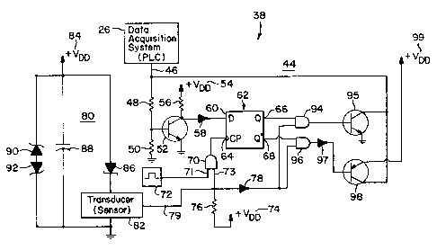
As shown in Fig. 3, the circuitry of magnetic
proximity sensor 38, which includes logic selection
circuit 44, is electrically coupled to a data acquisition
system shown in this specific context as ~cy~ammable
logic controller 26. Logic selection circuit 44 comprises
a communication interface 46 which can accommodate full
duplex digital communication between the logic selection
circuit and ~LG~ammable logic controller 26.
Communication interface 46 connects to a first terminal of
resistor 48, whieh serves as the upper half of a voltage
divider while in combination with resistor 50. The values
of resistors 48 and 50 should be sufficiently high enough
to keep any undesirable leakage current from programmable
logic controller 26 to a bare minimum. A second terminal
of resistor 48 is connected to a first terminal of
resistor 50 and to the base electrode of an input device,
which is shown in this embodiment as an NPN transistor 52.
The first terminal of resistor 50 is likewise connected to
the base electrode of NPN transistor 52. However, a
, CA 02211060 1997-07-22
second terminal of that resistor is connected directly to
ground, which completes the voltage divider network.
Acting together, resistors 48 and 50 apply a voltage
signal to the base electrode of NPN transistor 52. This
voltage signal has a voltage level comprising a
predetermined fraction of the voltage level present at
communication interface 46 (i.e., at the input terminals
of programmable logic controller 26).
In accordance with a conventional sinking or
common emitter configuration, the collector electrode of
NPN transistor 52 is connected to a power supply 54
through pull-up resistor 56 and the emitter electrode of
that device is connected directly to ground. When a
voltage signal of relatively high level is present at
communication interface 46 (i.e., at the input terminals
of ~LG~Lammable logic controller 26), the voltage divider
network comprising resistors 48 and 50 applies a voltage
signal of generally high level to the base electrode of
NPN transistor 52. In response, NPN transistor 52 assumes
a conductive state and its collector electrode voltage
sinks to ground (hereinafter identified as a LOW voltage
level). On the other hand, when a voltage signal of
relatively low level is present at communication interface
46 (i.e., at the input terminals of programmable logic
controller 26), the voltage divider network applies a
voltage signal of generally low level to the base
electrode of NPN transistor 52. In response, NPN
transistor 52 assumes a non-conductive state and its
collector electrode assumes a voltage level which
approximates the voltage magnitude of power supply 54
(hereinafter identified as a HIGH voltage level).
Accordingly, the collector electrode voltage of NPN
transistor 52 can assume two generally different voltage
levels, designated as HIGH and LOW, which allows the NPN
transistor to serve as the input device for logic
selection circuit 44.
CA 022ll060 l997-07-22
-16-
The collector electrode of NPN transistor 52 iS
further connected to the input terminal of a NOT gate 58,
which may be conventional in design and operation. The
output terminal of NOT gate 58 assumes a voltage level
which is the logical inverse of the level of the voltage
signal present at the collector electrode of NPN
transistor 52. This inverted voltage signal is then
applied to a data input line 60 of a data latch generally
designated by reference numeral 62, which may be
conventional in design and operation. Therefore, if the
voltage signal present at the collector electrode of NPN
transistor 52 iS at a HIGH level, NOT gate 58 applies a
voltage signal of LOW level to the data input line of data
latch 62. Moreover, if the voltage signal present at the
i5 collector electrode of NPN transistor 52 iS at a LOW
level, the NOT gate applies a voltage signal of HIGH level
to the data input line of data latch 62. It will be
appreciated that the data input line of data latch 62
assumes a HIGH voltage level when the voltage level of the
signal present at communication interface 46 (i.e., at the
input terminals of programmable logic controller 26) iS
relatively high. In similar fashion, the data input line
of data latch 62 assumes a LOW voltage level when the
voltage level of the signal present at communication
interface 46 (i.e., at the input terminals of programmable
logic ~,ol.L~oller 26) iS relatively low. Accordingly, the
voltage level present at data input line 60 of data latch
62 follows the voltage level of the signal p~-?nt at
communication interface 46 (i.e., at the input terminals
of programmable logic controller 26).
In addition to data input line 60, data latch 62
includes a clock line 64, an output line 66, and an
inverted output line 68. Data latch 62 will enter its
conventional sample mode only when the voltage signal
present at clock line 64 makes a triggering transition of
voltage level, which is a LOW-to-HIGH transition for a
posit~e-edge-triggered data latch and is a HIGH-to-LOW
CA 022ll060 l997-07-22
-17-
transition for a negative-edge-triggered data latch. When
a triggering transition occurs, data latch 62 detects the
transition and enters its sample mode, in which the data
latch transmits the voltage level of the ~ignal present at
data input line 60 to output line 66. Furthermore, data
latch 62 inverts the voltage level of the signal present
at its data input line and transmits this inverted signal
to its inverted output line 68 at that time.
On the other hand, when clock line 64 of data
latch 62 iS not making a transition that triggers its
sample mode, the latch remains in its conventional latch
mode, in which it locks the voltage signals present at its
output and its inverted output lines. Moreover, the latch
no longer samples the voltage signal present at its data
input line while it is in its latch mode.
Clock line 64 of data latch 62 receives its
voltage signal from the output terminal of AND gate 70. A
first input terminal 71 of AND gate 70 iS connected to a
clock pulse generator 72, which typically generates a
train of alternating HIGH and LOW voltage pulses in a
manner well known in the art. It will be appreciated that
clock 72 may include a delay me~h~nism of the type well
known in the art to satisfy any circuit timing requirement
of the present invention. A second input terminal 73 of
AND gate 70 is connected to a power supply 74 through
pull-up resistor 76, to the input terminal of a NOT gate
78, and to a control interface 79 which connects logic
selection circuit 44 with communication enable circuitry
80. The communication enable circuitry is shown in Fig. 3
as a conventionally-designed magnetic proximity switch.
In particular, communication enable circuitry includes
several circuit components comprising a solid-state sensor
82, a power supply 84, a shottky diode 86, a capacitor 88,
and two opposing zener diodes 90 and 92. Solid-state
sensor 82 has three terminals. A first terminal receives
the sensor's required operating power from power supply 84
to which it is connected through shottky diode 86. A
CA 02211060 1997-07-22
-18-
second terminal is tied directly to ground and a third
terminal is connected to logic selection circuit 44 by
control interface 79, which allows the sen~or to transmit
an enable signal to the logic selection circuit upon
sensation of an external stimulus, which, in the described
application, is the nearby magnetic field resulting from
the close proximity of permanent magnet 38a when movable
piston 17 is at finishing end 24 of rodless cylinder 12
(see Fig. 2).
Shottky diode 86, capacitor 88, and opposing
zener diodes 90 and 92 all serve as protection for solid-
state sensor 82. In particular, shottky diode 86 prevents
reverse polarity from being placed across the terminals of
the sensor, capacitor 88, which is tied in parallel to the
combination of the shottky diode and the sensor, decouples
the sensor from any ac voltage that might be inadvertently
drawn from power supply 84, and opposing zener diodes 90
and 92, which are also tied in parallel to the combination
of the shottky diode and the sensor, limit the maximum
voltage applied across the sensor.
Communication enable circuitry 80 serves as the
control mechanism for logic selection circuit 44. In
particular, when communication enable circuitry 80 does
not send an enable signal to logic selection circuit 44
(i.e., when movable piston 17 is far enough away from
fj nichi ng end 24 of rodless cylinder 12 so that solid-
state sensor 82 does not detect the presence of a nearby
magnetic field resulting from permanent magnet 38a (see
Fig. 2)), the C~conA input terminal 73 of AND gate 70
assumes a HIGH voltage level, which approximates the
voltage magnitude of power supply 74, and the gate's
output terminal will therefore follow the voltage level of
the alternating pulse train generated by clock 72. Under
those circumstances, clock line 64 of data latch 62 is
driven by clock 72. As a result, data latch 62
periodically enters its sample mode coincident with each
alternate transition cf the clock and samples the voltage
' ' CA 02211060 1997-07-22
--19--
signal present at data input line 60 which, as described
above, follows the voltage signal present across the input
terminals of programmable logic controller 26.
In the alternative situation wherein
communication enable circuitry 80 sends an enable signal
to logic selection circuit 44 (i.e., when movable piston
17 is close enough to finishing end 24 of rodless cylinder
12 so that solid-state sensor 82 detects the presence of a
nearby magnetic field resulting from permanent magnet 38a
(see Fig. 2)), the second input terminal 73 of AND gate 70
assumes a LOW voltage level. In response, the output
terminal of AND gate 70 and, likewise, clock line 64 of
data latch 62 both assume LOW voltage levels. Because no
triggering transition of clock line 64 will occur under
those circumstances, data latch 62 will remain in its
latch mode and will no longer sample data input line 60.
Instead, the latch will retain the re~a~ive voltage
signals present on its output and inverted output lines 66
and 68 until communication enable circuitry 80 once again
fails to send an enable signal to logic selection circuit
44 (i.e., when movable piston 17 moves far enough away
from finishing end 24 of rodless cylinder 12 so that
solid-state ~en~or 82 no longer detects the presence a
nearby magnetic field resulting from permanent magnet 38a
(see Fig. 2)), thereby causing the latch to periodically
reenter its sample mode.
While latch 62 periodically enters its sample
mode, the input to NOT gate 78 assumes a HIGH voltage
level which approximates that of power supply 74. In
response, the output terminal of NOT gate 78, which is
connected to one input terminal of AND gate 94, assumes a
LOW voltage level. Therefore, the output terminal of AND
gate 94 will also assume a LOW voltage level, regardless
of the level of the voltage signal present at the gate's
other input terminal. This LOW voltage level assumed by
the output terminal of AND gate 94 is applied to the base
, CA 02211060 1997-07-22
-20-
electrode of an NPN transistor 95 to render that device
non-conductive.
In addition to AND gate 94, NOT gate 78 is
connected to one input terminal of AND gate 96. As
described above, while latch 62 periodically enters its
sample mode, a signal of LOW voltage level is present at
the output terminal of NOT gate 78 and, likewise, at one
input terminal of AND gate 96. In response, the output
terminal of AND gate 96 is driven to a LOW voltage level,
regardless of the level of the voltage signal present at
its other input terminal. The output terminal of that AND
gate is connected to the input terminal of a NOT gate 97.
Here, the output terminal of NOT gate 97 assumes a HIGH
voltage level which is applied to the base electrode of a
PNP transistor 98 to render that device non-conductive.
Accordingly, when communication enable circuitry
80 does not send an enable signal to logic selection
circuit 44 (i.e., when movable piston 17 is far enough
away from finishing end 24 of rodless cylinder 12 so that
solid-state sensor 82 does not detect the presence of a
nearby magnetic field resulting from permanent magnet 38a
(see Fig. 2)), data latch 62 periodically enters its
sample mode. Moreover, NPN transistor 95 and PNP
transistor 98 are both rendered non-conductive.
In the alternative situation wherein data latch
62 remains in its latch mode, the input terminal to NOT
gate 78 assumes a LOW voltage level, which is inverted to
a HIGH voltage level by the gate and then applied to one
input terminal of AND gate 94. The other input terminal
of AND gate 94 is connected to output line 66 of data
latch 62. Thus, the output terminal of AND gate 94 will
follow the voltage level of the signal present at output
line 66 under these circumstances and will apply a signal
of that voltage level to the base electrode of NPN
transistor 95. In similar fashion, the output terminal of
NOT gate 78 is also connected to one input terminal of AND
gate 96. The other input terminal of AND gate 96 is
CA 02211060 1997-07-22
-21-
connected to inverted output line 68 of data latch 62.
Therefore, the output terminal of AND gate 96 will follow
the voltage level of the signal present at inverted output
line 68 under these circumstances and will apply a signal
of that voltage level to the input terminal of NOT gate
97, which inverts the voltage level of that signal and
transmits the inverted signal to the base electrode of PNP
transistor 98. It will be appreciated that the level of
the voltage signal present at the base electrode of PNP
transistor 98 is equivalent to the level of the voltage
signal present at the base electrode of NPN transistor 95
while data latch 62 remains in its latch mode. In
particular, the base electrodes of both transistors are
set to a HIGH voltage level if a signal having a
relatively high voltage level was present at communication
interface 46 (i.e., across the input terminals of
programmable logic controller 26) when the final sample of
data input line 60 was taken before communication enable
circuitry 80 transmitted an enable signal to logic
selection circuit 44 (i.e., just prior to when movable
piston 17 is positioned close enough to fini-c~ing end 24
of rodless cylinder 12 so that solid-state sensor 82
detects a nearby magnetic field resulting from permanent
magnet 38a (see Fig. 2)). Likewise, the base electrodes
of both transistors are set to a LOW voltage level if a
signal having a relatively low voltage level was present
at the communication interface (i.e., across the input
terminal~ of programmable logic controller 26) when the
final sample of data input line 60 was taken (i.e., just
prior to when movable piston 17 is positioned close enough
to finishing end 24 of rodless cylinder 12 so that solid-
state sensor 82 detects a nearby magnetic field resulting
from permanent magnet 38a (see Fig. 2)).
In accordance with a conventional sinking
configuration, the emitter electrode of NPN transistor 95
is tied to ground and its collector electrode is tied to
communication interface 46 (i.e., across the nput
CA 02211060 1997-07-22
-22-
terminals of programmable logic controller 26).
Therefore, if a signal having a relatively high voltage
level is present at the communication interface (i.e.,
across the input terminals of programmable logic
s controller 26) when data latch 62 exits ita sample mode
and enters its latch mode (i.e., when communication enable
circuitry 80 sends an enable signal to logic selection
circuit 44 solid-state sensor 82 detects a nearby magnetic
field resulting from permanent magnet 38a (see Fig. 2)),
the base and collector electrodes of NPN transistor 95
initially assume a corresponding HIGH voltage level, which
renders that device conductive. NPN transistor 95 then
sinks the level of the voltage signal present at the
communication interface (i.e., across the input terminals
of programmable logic controller 26) to ground or a LOW
level while data latch 62 prevents the voltage signal
present at the communication interface (i.e., across the
input terminals of programmable logic controller 26) from
reassuming a HIGH voltage level. On the other hand, if a
signal having a relatively low voltage level is present at
the communication interface (i.e., across the input
terminals of programmable logic controller 26) when data
latch 62 exits its sample mode and enters its latch mode,
NPN transistor 95 is rendered non-conductive because of
the corresponding signal of LOW voltage level that is
applied to its base electrode throughout the latch mode
time period. Under these circumstances, NPN transistor 95
has no effect on-the level of the voltage signal present
at the communication interface (i.e., across the input
terminals of programmable logic controller 26).
In accordance with a conventional sourcing
configuration, the emitter electrode of PNP transistor 98
is tied directly to a power supply 99 and its collector
electrode is tied to communication interface 46 (i.e.,
across the input terminals of programmable logic
controller 26). Therefore, if a signal having a
relatively high voltage level is present at the
CA 02211060 1997-07-22
-23-
communication interface (i.e., across the input terminals
of programmable logic controller 26) when data latch 62
exits its sample mode and enters its latch mode (i.e.,
upon movement of movable piston 17 to a position
sufficiently close enough to finishing end 24 of rodless
cylinder 12 so that solid-state sensor 82 detects the
presence of a nearby magnetic field resulting from
permanent magnet 38a (see Fig. 2)), the base electrode of
PNP transistor 98 assumes a corresponding HIGH voltage
level throughout the latch mode time period. This renders
PNP transistor 98 non-conductive and therefore that device
has no effect on the level of the voltage signal present
at the communication interface (i.e., across the input
terminals of programmable logic controller 26). However,
if a signal of relatively low voltage level is present at
communication interface 46 (i.e., across the input
terminals of programmable logic controller 26) when data
latch 62 exits its sample mode and enters its latch mode
(i.e., upon movement of movable piston 17 to a position
sufficiently close enough to finishing end 24 of rodless
cylinder 12 so that solid-state sensor 82 detects the
presence of a nearby magnetic field resulting from
permanent magnet 38a (see Fig. 2)), PNP transistor 98 is
rendered conductive because of the corresponding signals
of LOW voltage level that are initially applied to its
base and collector electrodes. This conductivity of PNP
transistor 98 allows power supply 99 to source current to
communication interface 46, which causes the communication
interface to assume a HIGH voltage level ay~ oximating the
voltage magnitude of power supply 99. As a result, the
input terminals of programmable logic controller also
assume this same HIGH voltage level which approximates the
voltage magnitude of power supply 99. Data latch 62
prevents the communication interface (i.e., the input
terminals of programmable logic controller 26) from
reassuming a LOW voltage level under these circumstances.
CA 022ll060 l997-07-22
-24-
Accordingly, if a signal having a relatively
high voltage level i8 present at communication interface
46 (i.e., across the input terminals of programmable logic
controller 26) when data latch 62 exits its sample mode
and enters its latch mode (i.e., upon movement of movable
piston 17 to a position sufficiently close enough to
finishing end 24 of rodless cylinder 12 so that solid-
state sensor 82 detects the presence of a nearby magnetic
field resulting from permanent magnet 38a (see Fig. 2)),
NPN transistor 95 sinks the level of the voltage signal
present at the communication interface (i.e., across the
input terminals of programmable logic controller 26) to
ground until the latch reenters its sample mode (i.e.,
when movable piston 17 moves sufficiently far enough away
from finiching end 24 of rodless cylinder 12 SO that
solid-state sensor no longer detects the presence of a
nearby magnetic field resulting from permanent magnet 38a
(see Fig. 2)). On the other hand, if a signal having a
relatively low voltage level is present at communication
interface 46 (i.e., across the input terminals of
programmable logic controller 26) when data latch 62 exits
its sample mode and enters its latch mode (i.e., when
movable piston 17 moves sufficiently close enough to
finishing end 24 of rodless cylinder 12 so that solid-
2 5 state sensor detects the presence of a nearby magneticfield resulting from permanent magnet 38a (see Fig. 2)),
PNP transistor 98 allows power supply 99 to source current
to the communication interface, thereby driving the
voltage signal present at the communication interface
(i.e., across the input terminals to programmable logic
controller 26) to a HIGH level which approximates the
voltage magnitude of the power supply. Once data latch 62
reenters its sample mode (i.e., when movable piston 17
moves far enough away from finishing end 24 of rodless
cylinder 12 SO that solid-state sensor can no longer
detect the presence of a magnetic field resulting from
permanent magnet 38a (see Fig. 2)), NPN transistor 95 and
~ CA 02211060 1997-07-22
-25-
PNP transistor 98 both assume a non-conductive state,
thereby permitting communication interface 46 (i.e., the
input terminals of programmable logic controller 26) to
reassume its normal operating voltage level.
While a particular embodiment of the invention
has been shown and described, it will be obvious to those
skilled in the art that changes and modifications may be
made therein without departing from the invention in its
broader aspects, and, therefore, the aim in the appended
claims is to cover all such changes and modifications as
fall within the true spirit and scope of the invention.