Note: Descriptions are shown in the official language in which they were submitted.
CA 02211231 1997-07-23
1
DISTORTION COMPENSATION CONTROL FOR A POWER AMPLIFIER
This invention relates to the control of a distortion
compensation arrangement for a power amplifier, such as a
multi-channel linear power amplifier for a cellular radio
communications system:
Backaround of the Inven ion
As is well known, an RF amplifier operating at high
1o power levels has non-linear amplifier characteristics which
produce undesired intermodulation distortion due to
interaction between signals being amplified.
In order to compensate for the non-linear
characteristics, prior art systems provide distortion
compensation arrangements in which a part of the incoming
signal is subtracted, with appropriate delay, and phase and
gain adjustments, from a part of an amplified signal which
is subject to the non-linear amplifier characteristics to
2o isolate a distortion signal component. This distortion
signal is a form of compensation signal used to predistort
the main signal in order to compensate for the distortion
prior to amplification. Other known systems use a "feed
forward" arrangement where the compensation signal
comprises an adjusted copy of the original signal which is
used to compensate for the distortion after amplification.
Prior art systems, for example, those taught in United
States Patent No. 4,879,519 issued November 7, 1989, naming
Robert E. Myer as inventor, entitled "Predistortion
3o Compensated Linear Amplifier", and United States Patent No.
4,885,551 issued December 5, 1989, naming Robert E. Myer as
inventor, entitled "Feed Forward Linear Amplifier"
recognize the difficulty of controlling the compensation
because this requires modifying the gain and phase of the
compensation (e.g., the predistortion) signal component to
match the gain and phase shift of the amplified signal on a
continuing basis in order to compensate for changes in
operating conditions. To this end, these patents describe
CA 02211231 1997-07-23
2
the use of frequency scanning for sensing the presence of
an intermodulation signals. The system controls are then
adjusted in order to reduce such intermodulation signals
below a predefined threshold, using an iterative, trial and
error approach. In such systems, an initial adjustment is
made to the compensation signal. The output is then
frequency scanned in order to evaluate the results of the
initial adjustment. If such an adjustment does not reduce
the intermodulation signals below the threshold, another
to adjustment is made. The resulting intermodulation signal
detected by the frequency scanning process is then compared
with the previous intermodulation signal in order to
determine the next adjustment. This iterative approach is
continued until the intermodulation signals are below a
predefined threshold or a predetermined number of
adjustments have been made. Such an approach can take a
period of time while the iterative adjustments are made
before the intermodulation products are suitably reduced.
During this time period, unwanted distortion is potentially
2o produced by such a system.
There exists a need for a system which promptly
determines the gain and phase adjustments required for the
compensation signal to minimize the distortion signals
produced.
CA 02211231 1997-07-23
3
summary of the Invention
An object of.this invention is to provide a
compensation arrangement for a linear power amplifier which
adaptively controls the gain and phase of the compensation
signal component in order to reduce the total distortion
produced by the system.
Another object of the invention is to provide a
compensation arrangement which promptly determines the gain
1o and phase adjustments required for the compensation signal
to minimize the distortion signals produced.
The invention makes use of a reference signal, of
known frequency, which is amplified along with the desired
carrier signals. Such a system evaluates the errors
introduced to the known reference signal, and determines
the errors, (e. g., the intermodulation distortion) produced
by the amplification of the reference signal by the power
amplifier. These error signals are then used to determine
2o the actual adjustments to the compensation signal which
reduce the resulting error signals. Thus, a control loop
is introduced which, by reducing the distortion introduced
to the reference signal, reduces the overall distortion
introduced to the carriers.
Such a reference signal can be added to the carriers
prior to amplification and then subsequently canceled.
Alternatively, if the carriers to be amplified include a
suitable signal which is continuously present, such a
3o signal can be used as the reference signal. In the
preferred embodiment, the distortion (e.g., the
intermodulation products surrounding the reference signal
frequency) introduced to said reference signal is evaluated
by comparing an unamplified copy of the reference signal
with the reference signal component of the combined signal
amplified by the amplifier. A quadrature amplitude
modulation (QAM) demodulator is used for.this purpose. In
another embodiment of the invention, the distortion
CA 02211231 1997-07-23
4
introduced to the reference signal is evaluated by using an
FM discriminator centered at the known frequency of the
reference signal and an envelope detector.
According to one aspect of the invention, there is
provided a distortion compensation circuit for a power
amplifier comprising an input path for forwarding a
combined signal to the amplifier to form an amplified
signal, the combined signal comprising at least one carrier
1o and a reference signal; a compensation path for producing a
compensation signal for compensating for the distortion
produced by the amplifier; a control unit; coupler for
coupling the amplified signal to the control unit; the
control unit comprising error signal means for producing a
first difference signal indicative of the difference in
gain between the reference signal and an amplified
reference signal component of the amplified signal and for
producing a second difference signal indicative of the
difference in phase between the reference signal and the
2o amplified reference signal component; a gain and phase
adjuster, responsive the control unit, for adjusting the
gain and phase of the compensation signal in order to
minimize the error signals.
According to another aspect of the invention, there is
provided a method of minimizing the intermodulation
distortion produced by a RF power amplifier comprising the
steps of
(a) introducing an RF signal to be amplified, the RF
3o signal including a reference signal;
(b) producing a compensation signal which will largely
cancel the distortion produced by the RF power amplifier;
(c) producing a pair of error signals indicative of
the distortion introduced by the RF power amplifier to the
reference signal;
(d) adaptively adjusting the gain and phase of the
compensation signal in order to minimize the error signals.
CA 02211231 1997-07-23
Brief Describtion of the Drawinas
The present invention, together with further objects
and advantages thereof will be further understood from the
5 following description of example embodiments with reference
to the drawings in which:
Fig. 1 schematically illustrates one embodiment of the
invention incorporating a power amplifier with a
predistortion compensation arrangement;
to Fig. 2 schematically illustrates an amplifier and
predistortion compensation control arrangement in
accordance with an embodiment of the invention;
Figs. 3 and 4 show respectively a phase plane diagram
and a frequency spectrum diagram with reference to which
the operation of the arrangement of Fig. 2 is explained.
Fig. 5 illustrates a feed-forward arrangement used in
conjunction with the embodiment of Figures,l and 2.
Fig. 6 illustrates an alternative embodiment of the
control arrangement.
Detailed Describtion of the Preferred Embodiments
The preferred embodiment of the invention will be
described with respect to its implementation for
controlling a predistortion arrangement. It should be
appreciated that the control mechanism can also be suitably
adapted for use in controlling the .compensation signal used
in a feed forward system.
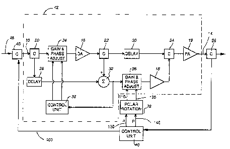
Referring to Fig. 1, there is illustrated~an input 48
3o for an RF signal to be amplified, a linear power amplifier
(PA) 12, couplers 46 and 26, an output 14 for an amplified
RF signal, a predistortion compensation arrangement which
is constituted by the components inside box 42, a control
arrangement 40 and a polar rotation unit 78. The RF signal
is, for example, a multi-channel signal including multiple
channels with frequencies within a portion of the 25 MHz
band from 869 to 894 MHz for use in a cellular radio
communications system. The distortion compensation
CA 02211231 1997-07-23
6
arrangement 42 serves to compensate for non-linear
characteristics of the amplifier 12, especially at higher
powers, thereby reducing intermodulation distortion among
the multiple channels.
The predistortion compensation arrangement comprises a
driver amplifier (DA) 16 which has characteristics closely
matched to those of the power amplifier 12; a further
amplifier 18; couplers (C) 20, 22, and 24; delay units 28
and 30; a subtracter 32; gain and phase adjustment units 34
and 36; and control unit 38 for controlling unit 34. The
predistortion and power amplifier arrangement (PD & PA)
within box 42 is known.
As shown in Fig. 1, control signals for gain and phase
adjustment unit 36, which originate from control unit 40
pass through polar rotation box 78.
Referring to box 42 of Fig. 1, the incoming signal
2o from the input 48 is coupled to a reference signal 100
originating from control unit 40 via coupler 46. This
combined signal 10 is then coupled to the input of the
power amplifier 12 via coupler 20; the gain and phase
adjustment unit 34, the driver amplifier 16, the coupler
22, the delay unit 30, and the coupler 24 in sequence. A
portion of the signal amplified by the driver amplifier 16
is coupled by the coupler 22 to an additive (+) input of
the subtracter 32, a subtractive (-) input of which is
supplied with a portion of the incoming signal l0 from the
3o coupler 20, after a compensating delay provided by the
delay unit 28. An output 33 of the subtracter 32 is
supplied as a feedback signal to the control unit 38, which
controls the gain and phase adjustment unit 34 to
substantially eliminate components of the incoming signal
at the output of the subtracter 32. Consequently, the
output 33 of the subtracter 32 is a distortion signal
component due to non-linearity or distortion in the driver
amplifier 16, corresponding (because of the close matching
CA 02211231 1997-07-23
7
of the amplifier 16 to the amplifier 12) to non-linearity
or distortion in the power amplifier 12. It should be
appreciated that the gain and phase adjustment unit 34
could alternatively be provided at other positions in
either of the input paths to the subtracter 32. The
arrangement shown has the advantage of positioning unit 34
in a feedback loop capable of compensating for gain
variations of amplifier 16 resulting from changes in
operating conditions, such as variations in temperature,
1o supply voltage, aging components, etc., which do not occur
in the path from 20 to 28 to 32.
Thus; elements 20, 34, 16, 22, 28, 32, and 38 serve
the primary function of producing distortion signal 33 as
the output of the subtracter 32 which closely approximates
the distortion added by amplifier 12, as is known in the
art. This distortion signal 33 is then used to predistort
the main signal to be amplified as follows.
2o This distortion signal 33 is then supplied, via the
gain and phase adjustment unit 36, to the amplifier 18 in
which the signal is amplified. The signal also undergoes a
180 degree phase shift, effectively inverting the signal,
in either the amplifier l8 or the adjuster 36. The output
of the amplifier 18 is supplied to the coupler 24, in which
the amplified distortion signal is subtracted (because of
its inversion) from the amplified combined signal (i.e:,
the output from DA16), the combined signal being provided
with a compensating delay in the delay unit 30. After the
subtraction in coupler 24, the predistorted signal is
supplied to the power amplifier 12.
Gain and phase adjustment unit 36 has two adjustable
input settings (or parameters). One parameter, which in
Fig. 1 is controlled by signal 110, adjusts the gain of the
distortion signal passing through the unit. The second
parameter, which in this case is controlled by signal 120,
adjusts the phase of the distortion signal passing through
CA 02211231 1997-07-23
g
the unit. The settings of gain and phase adjustments in
unit 36 are initially preset in order to produce a
distortion signal passing into amplifier 12 which will
largely cancel the distortion signal produced by amplifier
12, thus minimizing the intermodulation distortion at
output 14, as is known in the art.
A portion of the output signal 14 from the power
amplifier 12 is coupled by the coupler 26 back to the
control unit 40 to form a feedback loop, which controls the
gain and phase adjustment unit 36. This feed back loop
adjusts the settings of unit 36 in order to adaptively
compensate for changes in operating conditions, such as
variations in temperature, humidity, power supply voltage,
aging components, etc..
Two types of distortion which are produced by PA12 are
AM/AM (amplitude modulation to amplitude modulation
distortion) and AM/PM (amplitude modulation to phase
modulation distortion). For small errors in the settings
in unit 36, the effect on the composite non-linearity of
the entire system is as follows: errors in the gain
control signal 110 result in a composite non-linear
distortion of the same type (AM/AM or AM/PM) as that
produced by amplifiers 16 and 12, whereas errors in the
phase control signal 120 result in a composite non-linear
distortion of the opposite type as that produced by
amplifiers 16 and 12.
3o For example, let us assume amplifiers 16 and 12
produced only AM/PM (phase-rotation dependent on the input
signal envelope). For such an amplifier, an error in the
gain control signal 110 results in a composite AM/PM (same
type distortion) whose sign and magnitude are proportional
to the gain setting error, whereas an error in the phase
control signal 120 results in a composite AM/AM (RF gain
dependent on input signal envelope; i.e., opposite type
distortion) whose sign and magnitude are proportional to
CA 02211231 1997-07-23
9
the phase setting error. Similarly if amplifiers 16 and 12
only produced AM/AM distortion, then the gain control
signal 110 adjusts the composite AM/AM distortion and the
phase control signal 120 adjusts the composite AM/PM
distortion.
An amplifier typically exhibits both AM/AM and AM/PM
in some weighted combination. Therefore, an error in the
gain control setting 110 produces a similarly weighted
1o combination of AM/AM and AM/PM distortion and an error~in
the phase control setting 120 produces a differently
weighted combination of AM/AM and AM/PM distortion. For
the purposes of automating control in accordance with the
embodiment of the invention shown in Figs. 1 and 2, control -
unit 140 produces a pair of control signals (a, p), wherein
"a" is an AM/AM distortion compensation control signal, and
"p" is an AM/PM distortion compensation control signal, as
will be explained below. A polar rotation is applied to
the pair of control signals (a, p) produced by control unit
140, which is a complex number, in polar rotation unit 78
in order to produce the gain control signal 110 and the
phase control signal 120. This is done in such a manner
that changes in the "a" control signal results in largely
AM/AM distortion, and changes in the control signal "p"
results in largely AM/PM distortion. Polar rotation unit
78 produces gain control signal 110 = a * cos(theta) + p
sin(theta) and produces phase control signal 120 = a
sin(theta) - p * cos(theta), where theta is a fixed angle
selected according to the mix of AM/AM and AM/PM produced
3o by the amplifiers. For example, for amplifiers dominated
by AM/AM theta is close to zero degrees while for
amplifiers with mostly AM/PM, theta is close to 90 degrees.
For amplifiers which produce similar amounts of AM/AM and
AM/PM theta is close to 45 degrees. This actual setting
for theta in polar rotation unit 78 is set initially
depending on the characteristics of PA 12.
CA 02211231 1997-07-23
This invention is concerned particularly with the
manner in which the 'a' and 'p' signals, which are the
inputs into polar rotation unit 78, are produced, as
illustrated in Fig. 2. In Fig. 2, all of the components of
5 the arrangement of Fig. 1 inside box 42 are referred to as
a feed forward predistorter and power amplifier (PD & PA)
unit. Fig. 2 also shows polar rotation unit 78, initial
coupler 46 for producing input 10 from an initial input
signal 48 to the unit 42, the coupler 26, and the output 14
io of the arrangement of Fig. 1. The remaining components
illustrated in Fig. 2 serve as the control unit 40, as
shown in phantom.
Referring to Fig. 2, control unit 40 is shown to
include a pilot generator 44 which generates a pilot signal
100 at a frequency of, for example, 910 MHz, which serves
as the reference signal. This frequency is chosen for
convenience to be a little outside the signal band of the
input signal 48 which, for this example, is between 869 and
894 MHz), so that the intermodulation products, as
discussed below, can be more easily distinguished from the
desired signals. Coupler 46 serves to couple the pilot
signal from the generator 44, and the incoming RF signal
from the input path 48, to form the input signal 10 to the
unit 42.
As can be appreciated from the foregoing description,
the non-linear characteristics of the power amplifier
result in interaction between the RF signal being amplified
3o and the pilot signal. This interaction produces
intermodulation products at frequencies centered at the
pilot signal frequency, hereafter referred to as Reference
Intermodulation Products (RIPS), and intermodulation
products centered around the actual signals to be amplified
(hereafter referred to as Signal Intermodulation Products
(SIPs)), as shown in Fig. 4. The invention make use of a
specific reference signal, for example, the pilot signal to
isolate these RIPS in order to produce the feedback control
CA 02211231 1997-07-23
11
signals a and p which minimize the RIPS produced. As a
result of controlling the gain and phase adjustment unit 36
to minimize the RIPs produced, the SIPS produced by the
predistortion unit 42 are minimized.
To do this, the reference signal is split into two
paths. The first path is coupled to the incoming RF signal
and amplified along with it, forming amplified output
signal 14 as described above. This amplified signal is
to then QAM (Quadrature Amplitude Modulation) demodulated,
with respect to an appropriately phase-shifted copy of the
reference signal 44 (2nd path). As discussed below, this
produces appropriate precursors of the "a" and "p" control
signals; namely an "I" signal representing the gain change
in the reference signal after amplification in PA 12, and a
"Q" signal representing the phase change in the reference
signal: More particularly, the "I" signal,, which in this
embodiment is the first difference signal, is a signal
having a voltage which indicates the difference in gain, at
2o any given moment in time, between the reference signal and
the reference signal component of the amplified signal.
Similarly, the "Q" signal, which in this case is the second
difference signal, is a signal having a voltage which
indicates the difference in phase, at any given moment in
time, between the reference signal and the reference signal
component of the amplified signal. The second path is used
to control a feedback loop for controlling the QAM
demodulator.
3o In the embodiment shown in Fig. 2, the portion of the
output signal 14 which is coupled off by the coupler 26 is
supplied to a bandpass filter 50. Bandpass filter 50 has a
pass band centered at the pilot signal frequency and a
bandwidth corresponding to twice the bandwidth of the RF
signal being amplified, and substantially reduces the
amplitude of the amplified RF signal outside this pass
band. In other words, bandpass filter 50 serves to isolate
the RIPS. The output of the bandpass filter 50 is supplied
CA 02211231 1997-07-23
12
to a signal input of a QAM (Quadrature Amplitude
Modulation) demodulator 52. The QAM demodulator 52 also has
a local oscillator input which is supplied with the second
path of the pilot signal from the generator 44 via a phase
adjuster 56, which is controlled to adjust the phase of the
pilot signal as described below.
The QAM demodulator 52 produces in-phase (I) and
quadrature-phase (Q) demodulated output signals which are
1o supplied to optional low pass filters 58 and 60
respectively.
The I and Q demodulated signals produced at the
outputs of the QAM demodulator 52 track the in-phase and
quadrature-phase components of the pilot tone and its
intermodulation products as illustrated in Figs. 3 and 4.
Fig. 4 is a frequency spectrum diagram, illustrating,
by way of example, the relative amplitudes of different
2o frequencies of an RF multi-channel signal, the pilot
signal, and resulting intermodulation products of the RF
signal amplified via the unit 42. In this example, the
multi-channel signal comprises a plurality of RF carriers
constituting the desired signal, at frequencies in a
frequency band from 869 to 880 MHz. The bandwidth of the
RF signal in this case is thus 11 MHz. As is well known
for cellular radio communications systems, other RF carrier
frequencies and other RF signal bandwidths may equally be
used. Adjacent this desired RF signal band, at lower and
3o higher frequencies, Fig. 4 shows that there are signal
intermodulation products (SIPS) at lower amplitudes, these
being due to distortion (non-linearity) in the power
amplifier 12.
Fig. 4 also shows the pilot tone at a frequency of 910
MHz as described above, having an amplitude which is chosen
for example to be at -30 dBc with respect to the total
signal power. Also shown are reference intermodulation
CA 02211231 1997-07-23
13
products (RIPS) at lower amplitudes, at frequencies above
and below the pilot tone frequency, due to intermodulation
between the pilot signal and the RF carriers of the multi-
channel signal.
Fig. 4 also indicates a 22 MHz bandwidth of the
predominant RIPS centered around the pilot signal. In this
example, this 22 MHz bandwidth is equal to twice the RF
signal bandwidth of 11 MHz for a power amplifier having
1o conventional 3rd order non-linearity characteristics. In
this example, a suitable bandpass of filter 50 is 22 MHz in
order to isolate the RIPS and the low pass bandwidth of
filters 60 and 58 is 11 MHz. As a result of suitable
filtering, the QAM demodulator 52 is supplied with
substantially only the pilot tone and the intermodulation
products to which the pilot tone contributes; in other
words, the bandpass and lowpass filters reject the high-
amplitude RF carriers. Filters 58 and 60 may be omitted in
some circumstances, depending on the quality of QAM
demodulator 52, especially where the bandpass filter 50 is
present. These filters may also be supplemented with, or
replaced by, clipping, squaring, or other non-linear
circuitry for the purpose of compensating for higher order
distortion effects in the power amplifier 12.
Referring again to Fig. 2, the Q signal from LPF 60 is
preferably supplied via integrator 64 as a control signal
to the phase adjuster 56, thereby forming a control loop 65
to adjust the phase of the unamplified reference signal so
3o that this signal is in phase with the amplified reference
signal components (e.g. the RIPS) of the output 14 from the
amplifier 12. This control loop can be understood with
reference to Fig. 3. Fig. 3 is a phase plane diagram,
with axes representing in conventional manner the
amplitudes of the in-phase demodulated signal I and the
quadrature-phase demodulated signal Q produced at the
outputs of the QAM demodulator 52. A point P represents an
arbitrary position corresponding to the I and Q signal
CA 02211231 1997-07-23
14
magnitudes at an arbitrary time. This control loop serves
to move the point P in the direction of an arrow A along a
circular path (i.e. only the phase is changed) to the point
P1 on the I-axis, i.e. the d.c. value of Q is zero. When
phase shifter 56 is so adjusted, the Q signal is responsive
to phase changes through unit 42 and the I signal is
responsive to gain changes through unit 42.
A direct current (d.c.) component of the resulting I
signal is removed by a d.c. remover circuit 62. As
illustrated, the d.c. remover circuit 62 comprises a
subtracter 66 , a series resistor 68 and a shunt capacitor
70. The I signal is supplied to the additive (+) input of
the subtracter 66, and a smoothed or integrated version of
the incoming signal, produced by an integrator comprising
series resistor 68 and shunt capacitor 70, is supplied to
the subtracter's subtractive (-) input. Tl~e output of the
subtracter 66 constitutes the output of the d.c. remover
circuit 62. This output represents time varying
2o fluctuations in the gain of unit 42 caused by AM/AM non-
linearity.
A similar d.c. remover circuit 72 is supplied with the
output of an envelope detector 54, which serves to provide
a signal representative of the amplitude of the RF signal
envelope. As shown, the input to envelope detector 54 is
from coupler 26. It should be appreciated that the input
to the envelope detector 54 could alternatively be derived
from any point in the main RF signal path. The output
3o signals from d.c. remover circuit 62 and low pass filter 60
are each correlated with the RF signal envelope amplitude
by multiplying these signals by the output of the d.c.
remover circuit 72 in multipliers 74 and 76 respectively.
The Q demodulated signal, derived from the output of
the QAM demodulator 52 via the low pass filter 60 consists
of a variable signal which indicates the AM/PM (amplitude
modulation to phase modulation) distortion in the amplified
CA 02211231 1997-07-23
reference signal produced by the power amplifier 12. This
AM/PM distortion is represented in Fig. 3 by fluctuations
of the point P1 in the directions shown by a double-headed
arrow B. Thus the point P1 moves as indicated by the arrow
5 B along part of the circular path: This movement
corresponds to the phase modulation of the amplified
reference signal resulting from the amplitude modulation of
the main RF signal and the non-linear distortion of the
power amplifier 12.
to
This amplitude-dependent phase variation is correlated
with the amplitude of the RF signal envelope by the
multiplier 76, which multiplies the output of the low pass
filter 60 by the output of the envelope detector 54 after
15 removal of its d.c. component by the d.c. remover circuit
72. The output of the multiplier 76 constitutes an AM/PM
estimate or error signal whose average value is indicative
of thg sign and magnitude of the error in the AM/PM
distortion compensation control 'p'. This AM/PM error
2o signal determines both the magnitude and direction of the
phase adjustment to be made.
The I demodulated signal derived from the output of
the QAM demodulator 52 via the low pass filter 58 has its
d.c. component removed by the d.c. remover circuit 62. The
resulting signal indicates the AM/AM distortion produced by
the power amplifier 12 and is represented in Fig. 3 by
movement of the point P1 in the directions shown by a
double-headed arrow C. Thus the point P1 moves as
3o indicated by the arrow C radially with respect to the
intersection of the I and Q axes, corresponding to
amplitude modulation as a result of the amplitude
modulation of the main RF signal and the non-linear
distortion of the power amplifier 12. This amplitude
variation is correlated with the amplitude of the RF signal
envelope by multiplication of the outputs of the d.c.
remover circuits 62 and 72 in the multiplier 74. The
output of the multiplier 74, constitutes an AM/AM estimate
CA 02211231 1997-07-23
16
or error signal whose average value is indicative of the
sign and magnitude of the error in the AM/AM distortion
compensation control 'a'. This AM/AM error signal
determines both the magnitude and direction of the gain
adjustment to be made.
The resulting control signals are buffered in the
integrate and store unit 80 for controlling the gain and
phase adjuster 36 via polar rotation unit 78. It should be
io noted that the AM/PM and AM/AM detector sensitivity
approaches zero in the absence of either a RF carrier or
sufficient envelope fluctuations. Thus, integrate and
store 80 is preferably only updated if the main RF signal
is of sufficiently large average signal power and exhibits
sufficient envelope fluctuation. For example, a single FM
modulated carrier may have insufficient envelope
fluctuation, while the presence of two such FM carriers or
a single wideband amplitude modulated carrier such as a
signal from a multi user IS-95 Code Division Multiple
2o Access base station is likely to provide sufficient
envelope fluctuation. If the integrator is updated when
there is no carrier or an insufficient envelope
fluctuation, the offset voltages can cause the integrated
signals to increase or decrease to the control limits.
This can potentially result in transient intermodulation
when additional carriers are added. In this situation,
this transient intermodulation is avoided by storing the
integrator outputs when there is insufficient RF power or
envelope fluctuations. To this end, for example, updating
of the store 80 is enabled by an output of a compactor (not
shown) which compares the output of the envelope detector
54 with a fixed threshold level.
The arrangement described above operates on the
principle that a reference signal, e.g. the pilot signal,
added to the RF carriers, is subject to phase shift and
gain change in accordance with the instantaneous RF carrier
envelope and the non-linearity characteristics of unit 42.
CA 02211231 1997-07-23
17
Thus the reference signal is subject to an amplitude-
dependent phase shift and gain change (compression or
expansion). Demodulating the reference signal at the
output of unit 42 enables observation of the relationship
between the reference signal phase and gain and the
instantaneous RF envelope as detected at the output of unit
42. Multiplying the Q and RF envelope together provides an
AM/PM error signal. High pass filtering the L and RF
envelope terms and multiplying these together provides an
1o AM/AM error signal. The AM/PM and AM/AM error signals are
used to adjust the gain and phase of the compensating pre-
distortion signal in a feedback loop in order to minimize
the error signals, thereby providing optimal compensation
for the power amplifier distortion.
The predistortion arrangement discussed above is used
preferably in conjunction with a feed forward arrangement,
as illustrated in Fig. 5. This feed=forward circuitry
(comprising coupler 8, compensating delay 82, subtracter
84, phase inverting amplifier 92 and coupler 96, along with
compensating delay 94 for producing output 98, as is known
in the art) acts to cancel distortion which is not canceled
by the predistortion arrangement. Furthermore, after the
pilot has served its purpose in aiding predistortion
control, the feed-forward circuitry usefully serves to
largely cancel the pilot in output 98 via coupler 96; this
cancellation is optimized by adjusting the gain and phase
of the feed forward signal in gain and phase adjuster 88,
as is known in the art.
It should be noted that, as shown in Fig. 4, a pilot
signal frequency was chosen so that there is no
considerable overlap of the frequency band of the pilot
signal and its intermodulation products with the frequency
band of the RF carriers and their intermodulation products.
Any such overlap will reduce the effectiveness of the
bandpass filter(s), resulting in increased variability or
noise in the outputs of PD and PA unit 42. In order to
CA 02211231 1997-07-23
18
attenuate the RF carriers in this case and hence reduce
output variability, it is desirable to derive the input to
the QAM demodulator 52 from after a cancellation point
(e.g., after subtracter 84) of the feed forward path of the
system as shown in Fig. 5. Thus, Fig. 5 also shows a
coupler 86 for using the subtracted signal produced by
subtracter 84 as an alternative input (not shown) to QAM
demodulator 52 instead of the input as shown in Fig. 2. By
using this signal, the RF carriers are substantially
1o attenuated but with relatively little attenuation of the
reference signal from which the AM/AM and AM/PM estimates
are derived. As a result, variability in the outputs of PD
& PA unit 42 are reduced. In this case in particular, the
need for the bandpass filter 50 is reduced and thus can be
omitted.
It should be noted that although in Fig. 4 the pilot
signal is illustrated as a signal frequency tone, it should
be appreciated by a person skilled in the art that the
2o reference signal can be modulated to spread its energy over
a wide frequency band, for example, using FM or spread
spectrum PSK (phase shift key) modulation.
Although a particular implementation of the control
arrangement has been described above, it should be
appreciated that several alternatives can be used. For
example, control loop 65 comprising integrator 64 can be
eliminated. Instead, phase adjuster 56 is preset based on
factory lookup tables determined by the actual frequency
3o chosen as the pilot signal. In this case a DC remover
circuit, similar to that shown at 62 will be used to move
the DC component from the output of low pass filter 60
prior to mixing in mixer 76.
Furthermore, rather than inserting a pilot signal as a
reference signal, the reference signal can be extracted
from the input signal bandwidth. For example, the
reference signal can be selected to be a carrier usually
CA 02211231 2000-12-O1
19
present in the RF signal, such as a beacon or control channel.
If this approach is used then the bandpass filter 50 will not
be able to isolate the amplified reference signal as it is
part of the carrier. Consequently, the feed forward loop
approach shown in Fig. 5, using the output from coupler 86 as
the input to the QAM demodulator 52 is required. Also the
factory lookup table approach for presetting phase adjuster 56
will also be required.
It should also be appreciated that one or both of the
AM/PM and AM/AM error signals can be produced in other ways
without requiring a QAM demodulator, and in some control
arrangements only one of these error signals need be produced.
For example, the reader is directed to McNicol, et al, United
States Patent No. 5,193,224, issued March 9, 1993.
For another example, as shown in Fig. 6 in which the
pilot signal is at a separate frequency from the carriers, as
shown in Fig. 4, the AM/PM error signal can alternatively be
produced by integrating the output of an FM discriminator
centered at the pilot signal. Such a discriminator has its
input supplied with a signal derived from the output of the
bandpass filter 50.
Similarly, the AM/AM error signal is produced by removing
the DC from the output of an envelope detector whose input is
supplied with the output from bandpass filter 50.
The above description has shown various embodiments of
the invention directed to a predistortion arrangement and how
to control the gain and phase adjuster of such a predistortion
arrangement. It should be appreciated by a person skilled in
the art that such a control arrangement can also control the
gain and phase of a compensation signal which, rather than
being subtracted from the signal
CA 02211231 1997-07-23
to be amplified prior to amplification as in the
predistortion approach described above, as an alternative,
the compensation signal can be used to cancel distortion
introduced after amplification in a feed forward loop.
5
Numerous other modifications, variations, and
adaptations may be made to the embodiments of the invention
described above without departing from the scope of the
invention as defined in the claims.