Note: Descriptions are shown in the official language in which they were submitted.
CA 022113F74 1997-07-24
WAVEFORM GENERATOR
FIELD OF THE INVENTION
The present invention relates to the field of waveform generators for
producing waveforms for operating CRT displays and, more particularly, to a
s waveform generator for producing a horizontal or vertical dynamic focusing
voltage waveform.
BACKGROUND OF THE INVENTION
Devices as disclosed in Japanese Laid-open Patents S61-151591, Hl-
191895, and H4-114589 are well-known waveform generators for applying
0 dynamic focusing voltage to CRTs.
Fig. 6 is a block diagram of the major parts of a waveform generator
(dynamic focusing circuit) as disclosed in Japanese Laid-open Patent Hl-191895
as an example of the waveform generator of the prior art. The prior art comprises
a VCO (voltage control oscillator) 61, a binary counter 62, D/A (digital to analog)
converter 63, multiplication unit 64, and amplifier 65.
Operation of the prior art is briefly explained with reference to Fig.
6. The conventional waveform generator employs the clock pulse from the VCO
61 to make the binary counter 62 count synchronizing to the sc~nning frequency.
The D/A converter 63 receives the output of the binary counter 62 for producing a
20 saw tooth wave.
Then, the multiplication unit 64 multiplies the signal, after removing
CA 022113~4 1997-07-24
the direct current component from the saw tooth wave, by its inverted signal to
produce a parabolic waveform. The signal comprising a parabolic waveform
produced by the waveform generator is output as the dynamic focusing voltage.
As described above, the waveform generator of the prior art, in
s general, employs a multiplication unit for converting a saw tooth wave
synchronized to the sc~nning frequency to a signal comprising a parabolic
waveform. The parabolic waveform signal which has its minimllm value at the
center is then amplified to generate a dynamic focusing voltage waveform.
With increasing flatness of a CRT display screen, the optimal
o dynamic focusing voltage waveform is tending towards being in proportion to the
distance from the screen center raised for example to the 2.8th power, whereas aparabolic waveform, which has its minimllm value at the center, is plo~ollional to
the square of the distance from the screen center.
Therefore, the waveform generator of the prior art which generally
S produces a parabolic waveform is becoming unsuitable for producing the optimaldynamic focusing voltage waveform for more recent, flat-screen CRTs. The prior
art may fail to achieve the optimal focus characteristics over the entire screen.
This is a first disadvantage of the prior art.
The output waveform produced by a waveform generator is usually
20 several volts, but CRTs require several hundreds of volts as the dynamic focusing
voltage waveform.
Accordingly, the signal produced by the waveform generator needs
to be amplified for use by CRTs. To amplify the voltage at low cost, the focusing
circuit of the prior art employs a transformer to increase the voltage and supply
2s the increased dynamic focusing voltage waveform to the CRT.
The use of transformers, however, narrows the range of optimal
CA 022113~4 1997-07-24
frequency and phase characteristics of the focusing circuit. For example, if thefocusing circuit employs a transformer which is satisfactory around the horizontal
frequency of 100 kHz for amplifying the horizontal frequency around 30 kHz, the
actual dynamic focusing voltage may become asymmetric even though the
s waveform generator outputs a symmetric waveform. Comparing the left (L) and
right (R) from the center (C), as shown in Fig. 5, the actual dynamic focusing
voltage has distorted asymmetric waveform.
Therefore the waveform generator of the prior art may produce a
distorted dynamic focusing voltage waveform for some horizontal frequencies
when it is required to process a broad range of horizontal frequencies such as the
case with the latest CRT display monitors for computers.
The prior art may have difficulty in assuring the optimal dynamic
focusing characteristics for the entire range of horizontal frequencies. This is the
second disadvantage of the prior art.
SUMMARY OF THE INVENTION
The present invention employs a conversion unit which produces a
dynamic focusing voltage waveform for CRTs.
The conversion unit converts a position signal corresponding to the
position on the CRT screen to a converted signal which may be optimal dynamic
20 focusing voltage for CRTs.
A waveform of the converted signal may require modification to
correct deterioration or deformation of the waveform caused by the dynamic
focusing output circuit applied used over a broad synchronizing frequency range.
For this purpose, the present invention employs a correction unit for
25 selecting an appropriate constant for the conversion unit and correction unit itself,
CA 022113~4 1997-07-24
and thereby correcting the converted waveform, which is made by converting the
position signal, to make a corrected position signal.
The corrected position signal is reconverted using the same
conversion unit to produce the expected dynamic focusing voltage waveform.
s Thus, the waveform generator of the present invention enables the supply of anoptimal dynamic focusing voltage waveform over a broad synchronizing
frequency range.
BRIEF DESCRIPTION OF THE DRAWINGS
Fig. l(a) is a block diagram of a waveforrn generator in accordance
with a first exemplary embodiment of the present invention.
Fig. l(b) is a block diagram of a waveform generator in accordance
with a second exemplary embodiment of the present invention.
Fig. 2 is a block diagram of a waveform generator in accordance
with a third exemplary embodiment of the present invention.
Fig. 3 is a graph illustrating an example of characteristics of a
conversion unit 11 .
Fig. 4 is a graph illustrating exemplary waveforms.
Fig. 5 is an example of a focusing output with unfavorable
frequency and phase characteristics.
Fig. 6 is a block diagram of a waveform generator in accordance
with the prior art.
DESCRIPTION OF THE PREFERRED EMBODIMENTS
First exemplary embodiment
CA 022113~4 1997-07-24
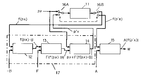
Fig. l(a) is a block diagram of a waveform generator in accordance
with a first exemplary embodiment of the present invention.
The waveform generator of the present invention uses a position
signal value px, offset coefficient -B, a coefficient F for correcting the scanning
s frequency, and an amplifying coefficient A for generating the dynamic focusingvoltage waveform output. The present invention first prepares a saw tooth wave
signal corresponding to the position on the screen for producing a dynamic
focusing voltage waveform. This is hereafter called the position signal px.
Configuration of the first exemplary embodiment is explained with
reference to Fig. l(a). The position signal px is input to a conversion unit 11
which generates a specified exponential function, for example px2 8. A first
addition unit 12 adds the output of the conversion unit 11 and the offset coefficient
-B. A first multiplication unit 13 multiplies the output of the first addition unit 12
by the sc~nning frequency correcting coefficient F. A second addition unit 14 adds
15 the output of the first multiplication unit 13 and the position signal px. The
conversion unit 11 again receives the output of the second addition unit 14. A
second multiplication unit 15 then multiplies the output of the conversion unit 11
by the amplitude coefficient A. The addition unit 12, first multiplication unit 13,
and second addition unit 14 form a correction unit 17.
Switches 16A and 16B are provided to inter-switch the input and
output of the conversion unit 11. When the position signal px is input to the
conversion unit 11, the first addition unit 12 receives the output of the conversion
unit 11. When the output of the second addition unit 14 is input to the conversion
unit 11, the second multiplication unit 15 receives the output of the conversionunit l l .
The position signal px is obtainable from a saw tooth wave produced
by a digital binary counter, ~as in the prior art. It can alternatively be obtained by
CA 022113~4 1997-07-24
converting the waveforrn of a saw tooth wave, which linearly decrease or increase
during CRT sc~nning, to a digital signal using an A/D converter.
The position signal corresponds to the sc~nning position (or data
point) x on the screen. The position signal has the minimllm value -P at the
s starting edge on the screen, O at the screen center, and the maximum value +P at
the ending edge of the screen.
The scanning position (or data point) x takes a value -n at the
starting edge of the screen, O at the screen center, and n at the ending edge of the
screen. In other words, the center value of the saw tooth wave corresponds to the
o screen center.
The position signal at each data point x (-n .. -1, O, 1, .. n) is
set as px.
The position signal px is input to the conversion unit 11, and the
conversion unit 11 outputs a corresponding functional value f(px) to the first
lS addition unit 12. The px is considered to be a normalized value because the value
of the position signal px later becomes the basis for correction and amplification
before output.
To support f(O) = O, f (-P) = f(+P), the input signal of the
conversion unit is converted to an absolute value at an input unit of the conversion
unit l l so that the conversion unit 11 always conducts operation on a positive
input value.
The conversion unit 11 comprises a memory for storing function
values. This memory desirably employs the input signal as a variable and stores
values in a part of the first quadrant near the origin of settable exponential
iùnction and those mirrored to the second quadrant symmetrical to the axis.
CA 022113~4 1997-07-24
In other cases the conversion unit comprises an absolute value circuit
for converting the input value to an absolute value and a memory for storing that
function values in a part of the first quadrant near the origin of a specified
exponential function which employs the input signal converted to an absolute
s value as a variable.
The first addition unit 12 and the second addition unit 14 can be
either a digital adder or an analog processor having a D/A converter unit.
In the same way, a first multiplication unit 13 and a second
multiplication unit 15 can be a digital multiplier or an analog multiplier, if the
addition unit is configured with an analog circuit. Likewise, addition unit and
multiplication unit can be configured in required combinations.
Table 1 is an example of the conversion unit 11 having the exponent
2.8 when P=253 and f(+P) = 63. Fig. 3 is a graph illustrating the values in Table
1.
px f(px) px f(px) px f(px) px f(px)
0 0 155 16 199 32 230 48
58 1 158 17 201 33 231 49
74 2 162 18 203 34 233 S0
3 165 19 205 35 235 51
4 168 20 207 36 236 52
102 5 171 21 209 37 238 53
109 6 174 22 211 38 239 54
l lS 7 177 23 213 39 241 SS
121 8 179 24 215 40 243 56
126 9 182 25 217 41 244 57
131 10 184 26 219 42 246 58
136 11 187 27 221 43 247 59
140 12 189 28 223 44 249 60
144 13 192 29 224 45 250 61
148 14 194 30 226 46 252 62
152 15 196 31 228 47 253 63
CA 022113~4 1997-07-24
The offset coefficient -B is pre-input to the first addition unit 12.
The output of the first addition unit 12 is
f (px) -B
This is input to the multiplication unit 13. The coefficient F is pre-
s input to the multiplication unit 13 as the sc~nnin,Q frequency correction coefficient.
The results of multiplication by the multiplication unit 13 is
F {f (px) -B}
This is input to the second addition unit 14.
The aforementioned normalized value px is also input to the second
o addition unit 14. The output of the second addition unit 14 is
px + F {f (px) -B}
This formula indicates that a position correction value
F {f (px) -B}
is added to the original normalized position signal px. If B = f (~P),
the position correction value
F {f (px) -B}
becomes 0 at the starting and ending edges of the screen, and the
minimllm value at the screen center. In other words, it can be understood that the
largest delay in the phase occurs at the screen center compared to the original
20 position signal px. This is defined as a corrected position signal:
p'x = px + F {f (px) -B}
The corrected position signal p'x is input to the conversion unit 11
CA 022113~4 1997-07-24
again, and the conversion unit 11 outputs the function value f (p'x). This is input
to the multiplication unit 15. Table 2 shows an example of details of operation up
to this point.
[Table 2] An example of conversion and calculation
s (When B = 63 and F = 0.77)
x px abs(px) f(abs(px)) f(px)-B F(f(px)-B) p'x abs(p'x) f(abs(p'x)
)
1 -255 255 64 1 1 -254 254 64
2 -220 220 43 -20 -16 -236 236 52
3 -185 185 26 -37 -28 -213 213 39
4 -150 150 15 -48 -37 -187 187 27
-115 115 7 -56 -43 -158 158 17
6 -80 80 3 -60 -47 -127 127 9
7 -45 45 1 -62 -48 -93 93 4
8 -10 10 0 -63 -49 -59 59
9 25 25 0 -63 -48 -23 23 0
1 -62 -48 12 12 0
11 95 95 4 -S9 -45 50 50
12 130 130 10 -53 -41 89 89 3
13 165 165 19 -44 -34 131 131 10
14 200 200 33 -30 -23 177 177 23
235 235 51 -12 -9 226 226 46
16 255 255 64 1 1 256 256 65
16 270 270 76 13 10 280 280 83
The constant A is pre-input to the multiplication unit 15 as an
amplitude coefficient, and the multiplication unit 15 outputs the result of
multiplication: Af (p'x). This is the dynamic focusing output:
W = Af (p'x) = Af [px + F {f(px) -B}]
o If the SC~nning frequency correction coefficient F is 0, W = Af
(px). This is merely the amplitude of a specified exponential waveform set in the
conversion unit 11 multiplied by the amplitude coefficient A.
CA 022113~4 1997-07-24
Therefore, the first exemplary embodiment of the present invention
solves the first disadvantage of the waveform generator of the prior art previously
described. More specifically, the first exemplary embodiment enables the
generation of an ideal dynamic focusing voltage waveform for increasingly flat
s CRT display monitors for which compensation using a parabolic waveform has
become difficult.
When the sc~nning frequency correction coefficient F increases, the
dynamic focusing output W deforms, generating the largest delay in the phase at
the screen center due to the effect of the corrected position signal p'x.
o Thus, the f1rst exemplary embodiment of the present invention
solves the second disadvantage of the waveform generator of the prior art
previously described by controlling the sc~nning frequency correction coefficient
F. In other words, the distortion of a waveform which is a problem caused by theemployment of a low-cost transformer in the prior art can be corrected optimally.
As explained above, the waveform generator of the present invention
solves the first disadvantage of the prior art by employing the function in which
the exponent can be specified for producing the ideal dynamic focusing voltage
waveform required for recent CRT display monitors which are becoming difficult
to satisfy using a parabolic waveform.
Furthermore, the waveform generator of the present invention is
capable of optimi7ing correction by selecting an appropriate constant: A, B, or F
for processors, which solves the second disadvantage of the prior art: that is,
distortion of waveform caused by the dynamic focusing output circuit which has
deficient frequency and phase characteristics.
Fig. 4 shows an example of changes in the dynamic focusing output
waveform when the value F is changed. When P = 0, the waveform is inclined
CA 022113~4 1997-07-24
towards the left. On the other hand, when F = 0.77, the waveform is inclined to
the right. The waveform generator of the present invention thus enables the
cancellation of any distortion generated by the dynamic focusing output circuit by
generating signals with such waveform. Furthermore, a waveform which is
s desirably bisymmetrical is obtained. As shown, it is preferred that the curve
minimllm coincide with the x-axis.
Second exemplary embodiment
The coefficients A, B and C can be pre-input to the first addition
unit 12, the first and the second multiplication unit 13, 15 using hard-wiring or
0 reading them stored in a memory. The coefficients A, B and C can be determinedby picture quality determination experiments ch~nging values of the coefficients.
In the above explanation, the input and output of single conversion
unit 11 are switched. However, it is also possible to provide two conversion unit
1 lA and 1 lB with the same function (or two different functions) as in Fig. lB.
Third exemplary embodiment
A third exemplary embodiment of the present invention is explained
with reference to a block diagram of Fig. 2.
The first and second exemplary embo(liment~ were explained
referring to a hardware circuit configuration. The third exemplary embodiment
20 may be implemented, for example, using a CPU.
In the waveform generator according to the second exemplary
embodiment of the present invention, a ROM 21 for storing function data, a RAM
23 for storing waveform data, and a CPU 24 for processing are connected to a bus20. The RAM 23 receives the output of a counter 22 which is initialized by the
2s synchronizing signal S. A D/A converter 25 receives the output of the RAM 23.
CA 022113~4 1997-07-24
The CPU 24 calculates the focusing voltage waveform data
corresponding to the position on the screen using the function data previously
stored in the ROM 21, and the result thereof is stored in the RAM 23.
The counter 22 reads out the waveform data corresponding to the
5 position on the screen from the RAM 23, and causes to output the dynamic
focusing voltage waveform.
An offset coefficient -B, scanning frequency correction coefficient
F, and amplitude coefficient A are stored in the internal register of the CPU 24,
ROM 21 or RAM 23 illustrated, or other memory not illustrated in the figure.
Needless to say, the CPU 24 may conduct more than one addition and
multiplication processing.
The functions ROM 21, RAM 23, and CPU 24 may be combined in
alternative arrangements. For example, the function data can be stored in a partof fixed program are~ ;n the CPU instead of using the ROM 21. The RAM can be
S substituted with a part of the main storage in the CPU. The counter 22 can also be
replaced with a DMA controller. The equivalent function can also be re~li7e-1 byusing a part of the main storage as the RAM 21 and RAM 23, and function data is
transferred by processing of the CPU 24.
In Fig. 2, a so-called refresh memory is configured by continuously
20 reading out data in a specified storage area of the RAM 23 by the counter 22. The
synchronizing signal S initializes the counter 22 for keeping the readout timing.
The CPU 24 sets the dynarnic focusing voltage waveform data to the specified
storage area of the RAM 23.
More specifically, the CPU 24 first produces a position signal px
2s corresponding to the sc~nning position x on the screen, which has the Illillil~llllll
value -P at the stating edge of the screen, 0 at the screen center, and the maximum
CA 022113~4 1997-07-24
value +P at the ending edge of the screen.
Next, the CPU 24 reads out the function data f (px) stored in the
ROM 21 based on the position signal px. The CPU 24 then calculates the
corrected position signal p'x = F {f (px) -B} using the offset coefficient -B and
s the sc~nning frequency correction coefficient F. Consequently, the original
normalized position signal px and the position correction value F {f(px) -B} areadded to obtain p'x = px + F{f(px) -B}. As already explained in the first
exemplary embodiment, it can be understood that the corrected position signal p'x
causes the largest phase delay at the screen center compared to the original
position signal px.
Then, the CPU 24 reads out the function data f(p'x) stored in the
ROM 21 based on the corrected position signal p'x, and calculates the dynamic
focusing output W = Af(p'x) = Af[px+F{f(px) -B}] using the amplitude
coefficient A.
The CPU 24 then writes a calculated value to the RAM 23.
By repeating this operation, a series of dynamic focusing output data
is completed in the specified area of the RAM 23.
As explained above, the waveform generator of the present invention
employs the function in which the exponent can be specified for solving the first
20 disadvantage of the prior art. More specifically, the present invention enables the
generation of an ideal dynamic focusing voltage waveform for the latest CRT
display monitors which are becoming difficult to fully compensate using a
parabolic waveform.
Furthermore, in the waveform generator of the present invention,
2s appropliate constants A, -B, and F for processors are selectable as required for
solving the second disadvantage of the prior art. More specifically, distortion
CA 022ll3~4 l997-07-24
14
caused by the dynamic focusing output circuit which has deficient frequency and
phase characteristics can be corrected optimally by selecting ap~ pliate constants
A, -B, and F.
Fig. 4 is an example of change in the dynamic focusing output
5 waveform when a value of the constant F is changed. When F = 0, the waveform
is inclined towards the left, and when F = 0.77, the waveform is inclined towards
the right. The waveform generator of the present invention thus enables the
cancellation of any distortion caused by the dynamic focusing output circuit by
generating signals with such waveform.
0 The third exemplary embodiment of the present invention can solvethe first and second disadvantages of the prior art as explained in the first
exemplary embodiment. In addition, the waveform generator of the third
exemplary embodiment can be realized by the use of a part or all of the CPU,
ROM, and RAM for controlling the entire CRT display monitor. Thus, the third
S exemplary embodiment offers a low-cost CRT display monitor with optimal
focusing performance.
Accordingly, the present invention solves a problem of a waveform
generator which produces a dynamic focusing waveform not suitable for CRTs
requiring non-parabolic waveform, and cancels distorted frequency and phase
characteristics of the output circuit. The present invention realizes a waveformgenerator which assures high-quality dynamic focusing characteristics.
In the exemplary embodiments, an example of the employment of
exponential function is explained in detail. The type of function is naturally
selected in accordance with the characteristics of CRT displays. It will be
recognized that other types of functions may be employed in accordance with the
present invention. The exemplary embodiments are also explained with the
precondition that the dynamic focusing voltage waveform is applied to the CRT in
CA 022113~4 1997-07-24
the horizontal deflecting direction. It will be appreciated that the same effect is
achieved by applying the waveform in the vertical direction. The exemplary
embodiments are also explained with the precondition of the use of a digital signal
and digital circuit. It will also be appreciated that the present invention can be
realized with the use of an analog signal and an analog circuit.
The exemplary embodiments described herein are therefore
illustrative and not restrictive. The scope of the invention being indicated by the
appended claims and all modifications which come within the true spirit of the
claims are intended to be embraced therein.