Note: Descriptions are shown in the official language in which they were submitted.
CA 02211454 1997-07-25
TITLE OF THE INVENTION
PLL circuit of display monitor
FIELD OF THE INVENTION
The present invention relates to a PLL (phase locked loop)
circuit used in a generating circuit of clock signal, a generating
circuit of horizontal drive pulse signal, or the like used in a
digital circuit in, for example, a display monitor.
BACKGROUND OF THE INVENTION
Recently, in a display monitor, digital circuits are used in
circuits for generating deflection correction waveforms for correct-
ing display distortion and others, and a PLL c~rcuit is used in a
clock signal generating circuit used in a digital circuit.
Conventionally, a horizontal drive pulse was generated in an analog
horizontal synchronizing circuit of an exclusive integrated circuit
(IC). However, when incorporating various functions of display
monitor into a digital IC, generation of horizontal drive pulse is
also accommodated in a same IC, and generation of horizontal drive
pulse requires to use the PLL circuit for multiplying the clock
signal used in the same digital circuit.
An example of such PLL circuit is shown in Fig. 4. In Fig.
4, when the frequency dividing ratio of a dividing circuit 4 is set
at a specified value N, and the PLL is in locked state, and output
signal of a VCO (voltage controlled oscillator) 3 is synchronized
- I -
CA 02211454 1997-07-25
with a reference signal entered in a phase comparator 1, and its
oscillation frequency is N times of the frequency of the reference
signal. In the PLL circuit, the frequency dividing ratio of the
dividing circuit 4 may be sometimes fixed, but it may be also
controlled by a CPU 5 depending on the frequency of the entered
reference signal as shown in the diagram.
In the PLL circuit, in order to decrease jitter generated
in the reproduced image shown in the display monitor due to phase
fluctuation or phase noise of the PLL circuit, it is preferred to
use an oscillator of an excellent frequency stability in the VCO.
Nhen an oscillator of an excellent frequency stability is used in
the VCO, the control sensitivity of the oscillation frequency of
the VCO is often lowered. Generally, since the voltage width to
be controlled is limited, the variable frequency range capable of
controlling the oscillation frequency of the YCO is narrow. For
example, the resonance type VCO high in frequency stability is
narrower in the controllable variable frequency range as compared
with the VCO of multi-vibrator type or ring oscillator type.
However, due to variations of constants of the parts being
used, the oscillation frequency oscillated by the VCO varies, and
the VCO often oscillates at a frequency exceeding an expected
frequency range. Therefore, when designing the circuit, it is
necessary to determine the stability of oscillation frequency in
consideration of variation of constituent parts used in the circuit.
By such designing, to the contrary, the stabi-lity of oscillation
-2-
CA 02211454 2006-09-06
-3-
frequency of VCO is lowered and the jitter performance
declines.
Accordingly, to suppress variations of oscillation
frequency, the circuit designers attempted to limit the VCO
composing parts to the parts particularly small in allowable
deviation, and adjust individually the oscillation frequency
in the production process by using variable capacity
capacitors or the like.
As a result, the cost of the appliances using such
circuits was raised, and the productivity was impaired.
SUMMARY OF THE INVENTION
A PLL circuit of the invention comprises frequency
detecting means for detecting a variable range of an
oscillation frequency of a VCO, a dividing circuit for
dividing the oscillation frequency of the VCO, memory means
for storing frequency data of the VCO preliminarily detected
by the frequency detecting means, and control means for
setting the dividing ratio of the dividing circuit so as to
operate the VCO at a frequency near the center of the
variable range of the oscillation frequency of the VCO on
the basis of the frequency data stored in the memory means.
By using this PLL circuit, it is possible to suppress jitter
phenomenon of image due to fluctuation of phase occurring in
the PLL circuit.
In accordance with another broad aspect, the invention
provides a setting method of frequency dividing ratio of a
PLL circuit. The method comprises a step of detecting
frequency ft of reference signal for test, a step of
sequentially changing the frequency dividing ratio with
respect to said reference signal for test, a step of
detecting a frequency of output signal of a dividing circuit
CA 02211454 2006-09-06
-3a-
by said frequency detecting means at each frequency dividing
ratio, a step of confirming that the PLL is in locked state
by comparing the frequency of the reference signal for test
and the frequency of output signal of the dividing circuit,
a step of determining and storing a maximum value and
minimum value of the frequency dividing ratio for the PLL to
maintain the locked state, a step of calculating and storing
a central value Nc of the frequency dividing ratio from the
maximum value and minimum value of said frequency dividing
ratio, a step of detecting frequency fH of reference signal
to be entered in normal operation, a step of calculating the
frequency dividing ratio from the central value Nc of the
frequency dividing ratio of the frequency fH of the
reference signal to be entered and the frequency ft of the
reference signal for test in the formula N = Nc*ft/fH, and a
step of setting the frequency dividing ratio of the dividing
circuit at frequency dividing ratio N.
In accordance with another broad aspect, the invention
provides a setting method of frequency dividing ratio of a
PLL circuit. The method comprises a step of detecting
frequency ft of reference signal for test, a step of
sequentially changing the frequency dividing ratio with
respect to said reference signal for test, a step of
detecting a frequency of output signal of a dividing circuit
by said frequency detecting means at each frequency dividing
ratio, a step of confirming that the PLL is in locked state
by comparing the frequency of the reference signal for test
and the frequency of output signal of the dividing circuit,
a -step of determining and storing a maximum value and
minimum value of the frequency dividing ratio for the PLL to
maintain the locked state, a step of storing a difference AN
from a preliminarily stored standard value Ntyp, by
calculating a central value Nc of the frequency dividing
CA 02211454 2006-09-06
-3b-
ratio from the maximum value and minimum value of said
frequency dividing ratio, a step of detecting frequency fH
of reference signal to be entered in normal operation, a
step of calculating the frequency dividing ratio from the
central value Nc of the frequency dividing ratio of the
frequency fH of the reference signal to be entered and the
frequency ft of the reference signal for test in the formula
N = Ntyp x ft/fH+ AN x ft/fH, and a step of setting the
frequency dividing ratio of the dividing circuit at
frequency dividing ratio.
BRIEF DESCRIPTION OF THE DRAWINGS
Fig. 1 is a block diagram of a PLL circuit in a first
embodiment of the invention.
CA 02211454 1997-07-25
Fig. 2 is a graph showing the control characteristic of a
VCO for explaining the first embodiment of the invention.
Fig. 3 is a block diagram showing a horizontal drive pulse
generating circuit of a display monitor in a second embodiment of
the invention.
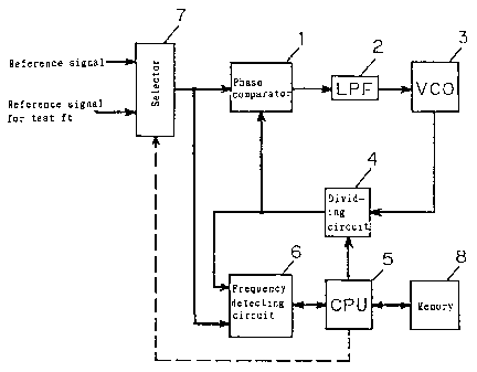
Fig. 4 is a block diagram of a conventional PLL circuit.
DESCRIPTION OF THE PREFERRED EMBODIMENTS
First exemplary embodiment
A first embodiment of the invention is described below by
referring to Fig. 1 and Fig. 2.
In Fig. 1, a phase comparator 1, a low,pass filter 2, a VCO
3, and a programmable counter (hereinafter called dividing circuit)
4 compose a general PLL circuit. A selector 7 changes over, by
control from a CPU 5, between a reference signal for test to be
entered when testing or installing a display monitor, and a
reference signal of normal operation, and issues to the phase
comparator 1. The phase comparator 1 detects the phase difference
of the output signal of the selector 7 and the output signal of
the dividing circuit 4, and issues the detected output voltage to
the.low pass filter 2. The detected output voltage filters and
attenuates the high frequency components in the low pass filter 2,
and is applied to the VCO 3 as a control voltage at a frequency
oscillated by the YCO 3.
-4-
CA 02211454 1997-07-25
The dividing circuit 4 receives the output signal of the YCO
3, and divides the oscillation frequency of the VCO 3 by a specific
frequency dividing ratio, and enters into the phase comparator 1.
The frequency dividing ratio of the dividing circuit is set by the
CPU 5.
A frequency detecting circuit 6 detects the frequency of the
reference signal and the output signal of the dividing circuit 4.
That is, the frequency detecting circuit 6 detects the frequency
of the reference signal which is an input signal to the display
monitor, and monitors the input signal, and the CPU 5 determines the
frequency dividing ratio of the dividing circuit 4 accordingly.
Moreover, the frequency detecting circuit 6 detects the
frequency of the reference signal and the output signal of the
dividing circuit 4, and sends out the result of detection to the CPU
5, while the CPU 5 confirms the locked state of the PLL.
Fig. 2 shows an example of frequency control characteristic
of the VCO. In Fig. 2, the axis of ordinates denotes the oscilla-
tion frequency of VCO. The axis of abscissas represents the control
voltage to the VCO, and its input control voltage is a voltage to be
applied to the VCO 3 through the phase comparator 1 and low pass
filter 2 in order to control the frequency oscillated by the VCO 3.
For example, line (a) shows the oscillation frequency
oscillated by a certain VCO accordingly when this VCO receives
control of control voltage. The above resonance type VCO shows such
characteristic. The left end (lower end) of the line indicates the
- 5 -
CA 02211454 1997-07-25
oscillation minimum frequency fmin of the VCO depending on the
minimum voltage Vmin of the control voltage applied to the YCO 3,
and the right end (upper end) of the line shows the oscillation
maximum frequency fmax of the YCO corresponding to the maximum
voltage Vmax of the control voltage applied to the VCO 3.
In Fig. 1, while the selector 7 is selecting the reference
signal for test, that is, while the PLL circuit is operating at the
reference signal for test at frequency ft, if the set frequency
dividing ratio is N, the oscillation frequency of the YCO 3 in the
locked state of PLL is ft x N. In the case of PLL locked state,
the frequency detecting circuit 6 detects the frequency of the
output signal of the dividing circuit 4, but the value of this
frequency is nearly same ft as the reference signal.
While the VCO is indicating the control characteristic in
Fig. 2 (a) and the input signal is operating by the reference signal
for test at frequency ft, the following measurement is carried out
in the PLL circuit.
The frequency dividing ratio of the dividing circuit 4 of
the PLL circuit is changed sequentially, and the frequency dividing
ratio at which the PLL is capable of maintaining the locked state
(therefore the frequency of the output signal of the dividing
circuit 4 is nearly ft) is measured. It is understood that the
oscillation frequency range of the VCO 3 corresponding to the
frequency dividing ratio from the lower limit value Nmin of the
measured frequency dividing ratio to the upper limit value Nmax is
6 -
CA 02211454 1997-07-25
from Nmin x ft to Nmax x ft. In the operation by the reference
signal for test, when the frequency dividing ratio of the dividing
circuit is selected in the median value of the lower limit value
Nmin and upper limit value Nmax, the operation of the PLL circuit
takes place nearly in the middle of the control range of the VCO.
In normal operation, considering the frequency ratio of
the frequency of reference signal for test and the frequency of
reference signal in normal operation, when the frequency dividing
ratio is set according to this frequency ratio, the operation of the
PLL circuit takes place nearly in the middle of the control range of
the VCO.
Thus obtained data and the data obtained by calculating them
are stored in the memory 8 as the measured VCO,frequency data.
In normal operation from the next time, the VCO frequency
data stored in the memory 8 is utilized, and the frequency dividing
ratio of the dividing circuit is determined according to the
reference signal to be entered.
In this way, corresponding to reference signals of various
frequencies, the oscillation frequency of the VCO 3 can be set
nearly in the middle of the control range for operation of PLL.
As the VCO frequency data, calculating the lower limit value
Nmin and upper limit value Nmax of the frequency dividing ratio in
the following formula. Nc may be stored in the memory 8.
Nc = (Nmin+ Nmax)/2
Incidentally, if the right side is a fraction, an integer counting
- 7 -
CA 02211454 1997-07-25
up or discarding the fraction is used as the Nc.
In next normal operation, the frequency dividing ratio N
to be set in the dividing circuit is the value calculated in the
following formula from the frequency data Nc of the VCO 3 being read
out from the memory 8, in terms of the frequency detection result fH
of the entered frequency signal.
N = Nc x ft/fH
The difference between Nc and, for example, design standard
value Ntyp, 0 N(= Nc - Ntyp) may be also stored in the memory 8.
In next normal operation, the frequency dividing ratio N to be set
in the dividing circuit is the value calculated in the following
formula from the frequency data AN of the VCO 3 being read out from
the memory 8, in terms of the frequency detection result fH of the
entered frequency signal.
N = Ntypx ft/fH+pNx ft/fH
In Fig. 2, when the frequency dividing ratio of the dividing
circuit is fixed and it is necessary to oscillate at a specified
frequency, considering the variation of the oscillation frequency of
the VCO, the YCO showing the control characteristic as shown in (b)
is required. The VCO showing such control characteristic is poor in
frequency stability, and is likely to be influenced by the control
voltage.
Such VCO changes the oscillation frequency depending on the
change of the control voltage due to a slight fluctuation of phase,
and significantly deteriorates the jitter characteristic. On the
_8-
CA 02211454 1997-07-25
other hand, the VCO showing the control characteristic as shown in
(a) is excellent in frequency characteristic, and is hence hardly
influenced by control voltage.
Such VCO is small in change of oscillation frequency
corresponding to the change of the control voltage due to fluctua-
tion of phase and is hence excellent in jitter characteristic.
Incidentally, when the design target is the characteristic
of (c) but the characteristic is actually (a) due to variation of
oscillation frequency, by setting the frequency dividing ratio of
the dividing circuit in every VCO, it is possible to operate the PLL
circuit in the middle of the control range.
Therefore, it is not necessary to match with the character-
istic of (c) by adjusting the oscillation freqpency individually in
every VCO, and the limitation of the allowable error of character-
istic value of the parts used in the VCO may be largely alleviated.
Of course, it is necessary to measure the oscillation
frequency of the YCO only once on a certain moment or occasion.
Detection of oscillation frequency range of the VCO may be done
alone if possible, but when checking the locking range of the PLL,
it is not necessary to apply certain voltage to the VCO from outside,
but it is convenient to process by the software alone.
Second exemplary embodiment
A second embodiment of the invention is described by
reference to Fig. 3. In Fig. 3, a horizontal drive pulse generating
- g -
CA 02211454 1997-07-25
circuit of display monitor is used as the PLL circuit of the
invention.
In Fig. 3, a selector 7 changes over, by the control of
a CPU 5, between a reference signal for test, and a reference
signal to be entered through a delay circuit 12 from a horizontal
synchronizing signal, and issues to a phase comparator 1.
The reference signal for test is an input signal used in
test or production process of display monitor, and it is mainly
generated by dividing a clock signal issued by a clock signal
generator composed of a quartz oscillation circuit for generating
operation clock of CPU in a dividing circuit 11. A general PLL
circuit is composed of phase comparator 1, low pass filter 2, VCO 3,
and drive pulse generating circuit 14, or of dfive pulse generating
circuit 14 and horizontal output circuit 9.
The phase comparator 1 detects the phase difference of the
output signal of the selector 7 and the output signal of the drive
pulse generating circuit 14 operating as dividing circuit, and
issues the detected output voltage to the low pass filter 2.
The detected output voltage filters and attenuates the high
frequency range in the low pass filter 2, and is applied to the VCO
3 as the control voltage at the frequency oscillated by the VCO 3.
The drive pulse generating circuit 14 operating as dividing
circuit receives the output signal of the YCO 3, divides the
oscillation frequency of the VCO 3 at a specified frequency dividing
ratio, and issues to the phase comparator 1. The frequency dividing
- 10 -
CA 02211454 1997-07-25
ratio of the dividing circuit is set by the CPU 5.
The drive pulse generating circuit 14 operating as dividing
circuit divides the output signal of the VCO 3, and issues the
divided output signal to a selector 10, and the output signal of the
drive pulse generating circuit 14 functions as the horizontal drive
pulse for driving the horizontal output circuit 9.
A frequency detecting circuit 6 detects the frequency of
the reference signal and the output signal of the dividing circuit
contained in the drive pulse generating circuit 14. That is, the
frequency detecting circuit 6 detects the frequency of the reference
signal which is an input signal to the display monitor, and monitors
the input signal, while the CPU can determine the frequency dividing
ratio of the dividing circuit accordingly.
Moreover, the frequency dividing circuit 6 detects the
frequency of the reference signal and the output signal of the drive
pulse generating circuit 14, sends out the result of detection to
the CPU 5. while the CPU 5 checks the locked state of the PLL.
The selector 10 selects either the divided output signal or
the flyback pulse. The divided output signal is a signal of divid-
ing the output signal of the VCO 3 in the drive pulse generating
circuit 14 operating as the dividing circuit. The flyback pulse is
one of the output signals of the horizontal output circuit 9, and
the output signal of the drive pulse generating circuit 14 is one of
the signals driving the horizontal output circuit 9 and issued by
the horizontal output circuit 9.
_ 11 -
CA 02211454 1997-07-25
The selector 10 selects the output signal being divided when
measuring the oscillation frequency of the VCO, and selects the
flyback pulse in normal operation.
By the PLL circuit of this circuit, if the circuit delay
of the horizontal output circuit 9 is changed due to effect of
temperature or the like, the phase of the flyback pulse can be kept
constant, and the horizontal screen position can be always fixed at
the phase determined by the delay circuit 12.
In this embodiment, the-reference signal for test is
obtained by dividing the clock for operating the CPU in the dividing
circuit 11, so that external input of reference signal for test is
not necessary. As clear from the explanation herein, on the basis
of the input from the frequency dividing circuit 6, by the control
of selector 7, selector 10, and drive pulse generating circuit or
dividing circuit, and calculation and setting of preferred frequency
dividing ratio, and the like, absorption of variations of oscilla-
tion frequency of YCO can be completely done automatically by the
software of the CPU.
Thus, according to the invention, if the oscillation
frequency of the VCO varies, it is possible to operate at the
optimum frequency depending on the oscillation frequency of each VCO,
and the design for using the VCO of stable frequency can be realized,
and therefore, while keeping low jitter, it presents a PLL circuit
minimizing the effects of variation of oscillation frequency of the
YCO on the cost and productivity
_ 12 -