Note: Descriptions are shown in the official language in which they were submitted.
CA 02212034 1997-08-01
BACKGROUND OF THE INVENTION
Field of the Invention
The present invention relates to a synchro-
nizer for a communication system, or more in particular
to a synchronizer in which a timing deviation can be
estimated based on the average value of the difference in
frame timing even in the case where a unique word (UW)
pattern fails to be received, thereby making it possible
to hold a frame timing even after a protracted line
disconnection.
Description of the Related Art
A conventional synchronizer of this type, as
shown in Fig. lA, comprises a UW pattern detection cir-
cuit 2, a reference timer 5, a latch circuit 6, a histo-
gram calculation circuit 8, a timing correction valuecalculation circuit 10, and a decoder 13. The UW pattern
detection circuit 2 detects a unique word pattern (here-
inafter referred to as "the UW pattern") contained in a
known symbol pattern (normally called "the synchronous
word" or "the unique word") of a receiving signal 1 shown
in Fig. lB. The reference timer 5 calculates the receiv-
ing time based on a reference clock 4. The latch circuit
6 fetches the time when the UW pattern is detected (the
UW pattern detection time) by latching an output signal
of the reference timer 5 by an output signal 3 of the UW
CA 02212034 1997-08-01
pattern detection circuit 2. The histogram calculation
circuit 8 calculates the histogram of the UW pattern
detection time from an output signal 7 of the latch
circuit 6 and further calculates the difference between
the frame timing of a transmitter and the frame timing of
a receiver based on the calculated histogram and an
output signal 12 of the timing correction value calcula-
tion circuit 10. The timing correction value calculation
circuit 10 produces on the basis of an output signal 9 of
the histogram calculation circuit 8 a control signal 11
to be output to the reference timer 5 for correcting the
frame timing of the receiver in the forward direction
when deviated backward of the frame timing of the trans-
mitter and backward when deviated forward of the frame
timing of the transmitter. Specifically, in correcting
the frame timing of the receiver in forward direction,
the initial value of the reference timer 5 is set to +1
by the control signal 11, while in correcting the frame
timing of the receiver backward, the initial value of the
reference timer 5 is set to -1 by the control signal 11.
In this way, the frame length is increased or decreased
by one frame, as the case may be, to set the frame timing
of the receiver to conform with that of the transmitter.
As described above, in the conventional syn-
chronizer, the frame timing of the receiver is correctedby detecting the UW pattern constantly and thus by de-
tecting the difference between the frame timing of the
receiver and that of the transmitter. As a result, in
CA 02212034 1997-08-01
the case where the UW pattern cannot be detected over a
long time due to a line disconnection or the like, the
frame timing of the receiver and that of the transmitter
are deviated considerably from each other.
SUMMARY OF THE INVENTION
The object of the present invention is to
provide a synchronizer in which the frame timing of the
receiver and that of the transmitter are prevented from
deviating from each other considerably even in the case
where a known symbol pattern fails to be detected over a
long time due to a line connection or the like.
In order to achieve the above-mentioned ob-
ject, according to the present invention, there is pro-
vided a synchronizer in which an average value of a
difference between a frame timing of a receiver and a
frame timing of a transmitter is calculated, the average
value of the difference in frame timing is integrated at
intervals of a predetermined frame time, and the timing
is corrected based on the integrated value of timing
deviations. Consequently, even in the case where the UW
pattern fails to be detected, the timing deviation can be
estimated based on the average value of the difference in
frame timing. Even in the case where the line is discon-
nected over a long time, therefore, the appropriate frame
timing can be held.
According to another aspect of the present
invention, there is provided a synchronizer which com-
CA 02212034 1997-08-01
prises a detection circuit for detecting a difference
between a reference timing of a transmitter and a refer-
ence timing of a receiver based on a time of receiving a
known transmission pattern transmitted from the trans-
mitter, an average value calculation circuit for calcu-
lating an average value of the detected difference, an
integration circuit for integrating the average value
each time of interrupting the receiver and determining an
integrated value, and a correction value calculation
circuit for correcting the reference timing of the re-
ceiver in forward direction in the case where the inte-
grated value is larger than a first threshold value and
correcting the reference timing of the receiver backward
in the case where the integrated value is smaller than a
second threshold value.
BRIEF DESCRIPTION OF THE DRAWINGS
Fig. lA is a block diagram showing a conven-
tional synchronizer.
Fig. lB is a diagram for explaining a frame
format.
Fig. 2 is a block diagram showing a synchro-
nizer according to a first embodiment of the present
invention.
Figs. 3A to 3D are diagrams for explaining the
operation of the synchronizer shown in Fig. 2.
Figs. 4A to 4D are diagrams for explaining the
operation of the synchronizer shown in Fig. 2.
CA 022l2034 l997-os-o
-- 5
Fig. 5 is a block diagram showing a synchro-
nizer according to a second embodiment of the present
invention.
Figs. 6A to 6D are diagrams for explaining the
operation of the synchronizer shown in Fig. 5.
Fig. 7 is a block diagram showing a synchro-
nizer according to a third embodiment of the present
invention.
Figs. 8A to 8E are diagrams for explaining the
operation of the synchronizer shown in Fig. 7.
Fig. 9 is a block diagram showing a synchro-
nizer according to a fourth embodiment of the present
invention.
Figs. lOA to lOE are diagrams for explaining
the operation of the synchronizer shown in Fig. 9.
Fig. 11 is a block diagram showing a synchro-
nizer according to a fifth embodiment of the present
invention.
Figs. 12A and 12B are diagrams for explaining
the operation of the synchronizer shown in Fig. 11.
Fig. 13 is a block diagram showing a synchro-
nizer according to sixth and seventh embodiments of the
present invention.
Fig. 14 is a diagram for explaining the opera-
tion of the synchronizer shown in Fig. 13.
Fig. 15 is a block diagram showing a synchro-
nizer according to an eighth embodiment of the present
invention.
CA 02212034 1997-08-01
Fig. 16 is a diagram for explaining the opera-
tion of the synchronizer shown in Fig. 15.
Fig. 17 is a block diagram showing a synchro-
nizer according to a ninth embodiment of the present
invention.
Fig. 18 is a diagram for explaining the opera-
tion of the synchronizer shown in Fig. 17.
Fig. 19 is a block diagram showing a synchro-
nizer according to a tenth embodiment of the present
invention.
Fig. 20 is a block diagram showing a synchro-
nizer according to an eleventh embodiment of the present
invention.
Fig. 21 is a block diagram showing a synchro-
nizer according to a twelfth embodiment of the presentinvention.
DESCRIPTION OF THE PREFERRED EMBODIMENTS
(First embodiment)
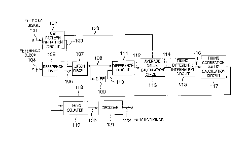
A synchronizer according to a first embodiment
of the present invention comprises, as shown in Fig. 2, a
UW pattern detection circuit 102, a reference timer 105,
a latch circuit 107, a D flip-flop (D-FF) circuit 109, a
difference circuit 111, an average value calculation
circuit 113, a timing difference integration circuit 115,
a timing correction value calculation circuit 117, a
timing counter 119 and a decoder 121.
The UW pattern detection circuit 102 detects a
CA 02212034 1997-08-01
UW pattern (Fig. lB) contained in a receiving signal 101.
Upon detection of the UW pattern, a UW pattern detection
signal 103 is output and a UW pattern detection infor-
mation signal 123, which indicates whether or not the UW
pattern is detected, is generated. The reference timer
105 calculates a receiving time based on a reference
clock 104. The latch circuit 107 latches an output
signal 106 of the reference timer 105 by the UW pattern
detection signal 103 from the UW pattern detection cir-
cuit 102 thereby to fetch a time (UW pattern detectiontime) when the UW pattern is detected. The D flip-flop
circuit 109 holds the UW pattern detection time fetched
into the latch circuit 107. The difference circuit 111
determines a difference (frame timing difference) between
a frame timing of the transmitter and a frame timing of
the receiver based on a difference between an output
signal 108 of the latch circuit 107 and an output signal
110 of the D flip-flop circuit 109. The average value
calculation circuit 113 updates an average value of the
frame timing difference calculated based on an output
signal 112 of the difference circuit 111 only when the
detection of the UW pattern is indicated by the UW pat-
tern detection information signal 123 from the UW pattern
detection circuit 102. The timing difference integration
circuit 115 integrates the average value of the frame
timing difference based on an output signal 114 of the
average value calculation circuit 113.
The timing correction value calculation cir-
CA 02212034 1997-08-01
cuit 117 produces a control signal 118 for the timing
counter 119 on the basis of an output signal 116 of the
timing difference integration circuit 115 in order to
correct the frame timing of the receiver in forward
direction in the case where it is deviated backward of
the frame timing of the transmitter on the one hand and
to correct the frame timing of the receiver backward in
the case where it is deviated forward of the frame timing
of the transmitter on the other hand. Specifically, in
the case where the frame timing of the receiver is cor-
rected in forward direction, an initial value of the
timing counter 119 is set to +1 by the control signal
118, while in the case where the frame timing of the
receiver is corrected backward, the initial value of the
timing counter 119 is set to -1 by the control signal
118. In this way, the frame length is increased or
decreased, as the case may be, by one frame thereby to
set the frame timing of the receiver to conform with the
frame timing of the transmitter. The timing counter 119
counts the reference clock 104 by a period of one frame
with the initial value set by the control signal 118 from
the timing correction value calculation circuit 117. The
decoder 121 generates various timings 122 based on an
output signal 120 of the timing counter 119.
Now, the operation of the synchronizer ac-
cording to this embodiment will be explained with refer-
ence to Figs. 3A to 3D. The receiving signal 101 inserts
therein the UW pattern for each frame as shown in Fig.
CA 02212034 1997-08-01
3A. The receiving signal 101 is transmitted based on the
frame timing of the transmitter. The one-frame time of
the transmitter can be detected, therefore, by detecting
the intervals at which the UW patterns contained in the
receiving signal 101 are received. In the receiver, UW
pattern detection time T(k+1) is detected by the value on
a timer built therein. The difference is determined
between UW pattern detection time T(k+1) detected in the
current frame and UW pattern detection time T(k) detected
in the previous frame thereby to determine the one-frame
time of the receiver (Fig. 3B). In fact, assuming that
the maximum count value of the timer is N (Fig. 3C), the
one-frame time of the receiver can be determined from the
modulo calculation shown below.
{T(k+1) + N - T(k)} modulo N (1-1)
The difference between the value determined by equation
(1-1) above and the standard frame time length consti-
tutes the difference between the frame timing of the
receiver and that of the transmitter.
The timing correction value calculation cir-
cuit 117 performs the following processes:
(1) The frame timing of the receiver, if deviated back-
ward of the frame timing of the transmitter by a set
value or more, is corrected in forward direction by the
set value.
(2) The frame timing of the receiver, if deviated in
forward direction from the frame timing of the transmit-
ter by a set value or more, is corrected backward by the
CA 02212034 1997-08-01
-- 10 --
set value.
(3) In the case where the deviation of the frame timing
of the receiver from that of the transmitter is not more
than the set value, then the frame timing of the receiver
is not corrected.
Assume that the set value is l and that the
frame timing of the receiver is required to be corrected
in forward direction by the set value. The initial value
of the timing counter 119 is set to +1. In the case
where the frame timing of the receiver is required to be
corrected backward by the set value, on the other hand,
the initial value of the timing counter 119 is set to -1.
In this way, the frame length is increased or decreased,
as the case may be, by one frame. Figs. 4A to 4D show an
example of correcting the frame timing of the receiver by
one in forward direction. This shows the manner in which
the timing generated is corrected in forward direction by
one by increasing the initial value of the timing counter
119 by one frame.
The average value calculation circuit 113
performs the following processes based on the UW pattern
detection information signal 123 from the UW pattern
detection circuit 102:
(1) The average value of the frame timing difference is
updated for the frame in which the UW pattern is detect-
ed.
(2) The average value of the frame timing difference is
not updated for the frame in which the UW pattern is not
CA 02212034 1997-08-01
detected.
As a result, even in the case where the UW
patterns are not detected continuously, the synchronizer
according to this embodiment can correct the timing using
the average value of the frame timing difference which is
not updated.
(Second embodiment)
A synchronizer according to a second embodi-
ment of the present invention, as shown in Fig. 5, is
different from the synchronizer according to the first
embodiment in that a timing counter 205 operates as the
reference timer 105 shown in Fig. 2 at the same time.
In the synchronizer according to the first
embodiment described above, the UW pattern receiving time
is detected using the reference timer 105. Consequently,
the clock rate of the timing counter 119 is normally the
same as the symbol rate or the bit rate. It is therefore
possible to detect the UW pattern receiving time with a
higher accuracy by increasing the clock rate of the
reference timer 105 as compared with that of the timing
counter 119. Such a synchronizer, however, requires two
counters for the reference counter 105 and the timing
counter 119, and therefore increases in circuit size and
power consumption.
In view of this, the synchronizer according to
this embodiment is adapted to detect the receiving time
of the UW pattern as well using the timing counter 205.
CA 022l2034 l997-08-Ol
- 12 -
As a result, a latch circuit 207 is supplied with an
output signal 206 of the timing counter 205. Also, in
order to compensate for the increase or decrease in an
output signal 212 of a difference circuit 211 due to the
detection of the UW pattern receiving time using the
timing counter 205, a D flip-flop (D-FF) circuit 221 for
holding a control signal 218 output from a timing cor-
rection value calculation circuit 217 is inserted between
the timing correction value calculation circuit 217 and
an average value calculation circuit 213.
A UW pattern detection circuit 202 detects a
UW pattern contained in a receiving signal 201. Upon
detection of the UW pattern, a UW pattern detection
signal 203 is output and a UW pattern detection infor-
mation signal 223, which indicates whether or not the UWpattern is detected, is generated. The latch circuit 207
latches the output signal 206 of the timing counter 205
by the UW pattern detection signal 203 from the UW pat-
tern detection circuit 202, thereby fetching a time when
the UW pattern is detected (UW pattern detection time).
A D flip-flop circuit 209 holds the UW pattern detection
time fetched into the latch circuit 207. The difference
circuit 211 determines a difference between the frame
timing of the transmitter and that of the receiver (frame
timing difference) based on the difference between an
output signal 208 of the latch circuit 207 and an output
signal 210 of the D flip-flop circuit 209. According to
this embodiment, the UW pattern detection time is detect-
CA 02212034 1997-08-01
ed using the timing counter 205 corrected in timing.
When the timing is corrected, therefore, the frame timing
difference determined by the difference circuit 211 is
increased or decreased by the amount of the timing cor-
rection. In view of this, the D flip-flop circuit 221
holds the control signal 218 from the timing correction
value calculation circuit 217, and the frame timing
difference determined by the difference circuit 211 is
corrected in the average value calculation circuit 213 in
accordance with the timing correction value indicated by
an output signal 222 of the D flip-flop circuit 221. The
average value calculation circuit 213 updates the average
value of the corrected frame timing difference only when
the UW pattern detection information signal 223 from the
UW pattern detection circuit 202 indicates that the UW
pattern is detected. A timing difference integration
circuit 215 integrates the average value of the frame
timing difference based on an output signal 214 of the
average value calculation circuit 213.
On the basis of an output signal 216 of the
timing difference integration circuit 215, the timing
correction value calculation circuit 217 generates the
control signal 218 for the timing counter 205 in order to
correct the frame timing of the receiver in forward
direction, if deviated backward of that of the transmit-
ter, and to correct the frame timing of the receiver
backward, if deviated forward of the frame timing of the
transmitter. Specifically, in the case of correcting the
CA 02212034 1997-08-01
- 14 -
frame timing of the receiver in forward direction, the
initial value of the timing counter 205 is set to +1 by
the control signal 218, while in the case of correcting
the frame timing of the receiver backward, the initial
value of the timing counter 205 is set to -1 by the
control signal 218. In this way, the frame timing of the
receiver is set to conform with that of the transmitter
by increasing or decreasing, as the case may be, the
frame length by one frame. The timing counter 205 counts
a reference clock 204 by frame period with the initial
value set by the control signal 218 from the timing
correction value calculation circuit 217. A decoder 219
generates various timings 220 based on the output signal
206 of the timing counter 205.
Now, the change in the UW pattern receiving
time due to the timing correction will be explained with
reference to Figs. 6A to 6D. As shown in Fig. 6A, the
receiving signal 201 inserts therein the UW pattern in
each frame thereof. In the shown example, the timing is
corrected during the period from the time when the second
UW pattern from the left is received to the time when the
third UW pattern is received. The initial value of the
timing counter 205 thus is set to +1 as shown in Fig. 6C.
The UW pattern detection time points fetched into the
latch circuit 207 the respective frames are assumed to be
t(k), t(k+1), t(k+2), t(k+3), respectively, as shown in
Fig. 6D. Assuming that the one-frame time of the trans-
mitter is identical to that of the receiver, the UW
CA 02212034 1997-08-01
pattern detection time points t(k), t(k+1), t(k+2),
t(k+3) for the respective frames have equal intervals.
Once the timing is corrected as described above, however,
the UW pattern detection time points t(k+2), t(k+3) for
the third and subsequent frames from the left in the
diagram are deviated to assume a value larger by one than
the UW pattern detection time points t(k), t(k+1) for the
first and second frames from left, respectively. Conse-
quently, the frame timing difference calculated by the
difference circuit 211 is given by the equation shown
below. It is seen that the timing difference between a
frame corrected in timing and the next frame is increased
by the timing correction value.
t(k+l) - t(k) = N (2-1)
t(k+2) - t(k+1) = N + 1 (2-2)
t(k+3) - t(k+2) = N (2-3)
The average value calculation circuit 213 subtracts the
timing correction value indicated by the output signal
222 of the D flip-flop circuit 221 from the frame timing
difference between a timing-corrected frame and the next
frame. As a result, the right frame timing difference is
obtained for all the frames. The UW pattern detection
time can thus be detected using the timing counter 205
for the timing correction.
(Third embodiment)
A synchronizer according to a third embodiment
of the present invention, as shown in Fig. 7, is differ-
CA 02212034 1997-08-01
ent from the synchronizer according to the first embodi-
ment shown in Fig. 2 in that a reference timer control
signal 324 is output to a reference timer 306 from a
decoder 322 and that a control signal 319 output from a
timing correction value calculation circuit 318 is ap-
plied also to the decoder 322.
In the synchronizer according to the first
embodiment described above, the reference timer 105 is
used for counting a period longer than the one-frame
time, while the synchronizer according to the second
embodiment uses the timing counter 205 for counting the
same period as the one-frame time. An increased number
of symbols or bits per frame is accompanied by an in-
creased number of bits of the counter, an increased
number of bits of the latch circuit, an increased number
of bits of the D flip-flop circuit for holding the UW
pattern detection time for the immediately preceding
frame and an increased number of bits of the difference
circuit, thereby leading to an increased power consump-
tion and an increased circuit size.
In view of this, in the synchronizer accordingto this embodiment, the reference timer control signal
324 is applied to the reference timer 306 from the decod-
er 322 in order to reduce the number of bits of the
counter making up the reference timer 306.
The basic operation of the synchronizer ac-
cording to this embodiment is similar to that of the
synchronizer according to the first embodiment. A method
CA 02212034 1997-08-01
of producing the reference timer control signal 324 will
be explained below.
The decoder 322 produces the reference timer
control signal 324 based on an output signal 321 of a
timing counter 320. This reference timer control signal
324, as shown in Figs. 8A to 8E, activates the reference
timer 306 a little before an assumed UW pattern receiving
time, and deactivates the reference timer 306 a little
after the assumed UW pattern receiving time. In the
process, as explained above with reference to the syn-
chronizer according to the second embodiment, in order to
correct the change in the UW pattern detection time
caused by the correction of the timing counter 320, the
decoder 322 corrects the time to activate the reference
timer 306 by the amount of correction value of the timing
counter 320 based on the control signal 319 of the timing
correction value calculation circuit 318.
The reference timer 306 is operated based on
the reference timer control signal 324 produced in the
manner described above thereby to produce the following
effects:
(1) The number of bits of the counter making up the
reference timer 306 can be reduced.
(2) The number of bits for calculation to detect the
frame timing difference can be reduced.
(3) The operation time of the reference timer 306 can be
reduced.
CA 022l2034 l997-08-Ol
- 18 -
(Fourth embodiment)
A synchronizer according to a fourth embodi-
ment of the present invention is different from the syn-
chronizer according to the third embodiment, as shown in
5 Fig. 9, in that a switch 406 iS provided on the input
side of a reference timer 408 for switching the applica-
tion and non-application of a reference clock 405 to the
reference timer 408 in accordance with a reference timer
control signal 426 from a decoder 424 and a UW pattern
detection signal 403 from a UW pattern detection circuit
402.
The synchronizer according to the third em-
bodiment described above activates the reference timer
306 a little before the assumed UW pattern receiving time
15 and deactivates the reference timer 306 a little after
the assumed UW pattern receiving time. In such a syn-
chronizer, however, the power consumption of the counter
constituting the reference timer 306 increases in the
following cases:
(1) In the case where the counter making up the refer-
ence timer 306 operates at a very high speed.
(2) In the case where the UW pattern receiving time
fluctuates to such an extent that the operation time of
the counter making up the reference timer 306 iS length-
ened.
In view of this, the synchronizer according tothis embodiment comprises the switch 406 and controls the
operation of the reference timer 408 in the following
CA 02212034 1997-08-01
-- 19 --
manner:
(1) The reference timer 406 is activated a little before
an assumed UW pattern receiving time.
(2) The reference timer 406 is deactivated upon detec-
tion of a UW patttern.
(3) The reference time 406 is deactivated a little after
the assumed UW pattern receiving time when a UW pattern
fails to be detected.
The basic operation of the synchronizer ac-
cording to this embodiment is similar to that of the
synchronizer according to the third embodiment described
above. A method of controlling the switching operation
of the switch 406 will be described. Assume that the
reference timer 408 is activated at the leading edge of
the reference timer control signal 426 from the decoder
424, as shown in Figs. lOA, lOD.
(1) In the case where a UW pattern is detected in the UW
pattern detection circuit 402:
The reference timer 408 is activated at the
leading edge of the reference timer control signal 426
from the decoder 424 (Figs. lOA to lOC). As a result, UW
pattern detection time T(k) is fetched into a latch
circuit 410 by the UW pattern detection signal 403 (Figs.
lOD, lOE). Also, the switch 406 is opened by the UW
pattern detection signal 403, so that the reference clock
405 stops being applied to the reference timer 408 and a
count value of the counter making up the reference timer
408 is reset (Fig. lOD). After that, the reference timer
CA 022l2034 l997-08-Ol
- 20 -
408 iS deactivated at the falling edge of the reference
timer control signal 426 ( Fig. lOD).
(2) In the case where a UW pattern is not detected in
the UW pattern detection circuit 402:
The reference timer 408 iS activated at the
leading edge of the reference timer control signal 426
from the decoder 424 ( Figs. lOA to lOC). In this case,
the UW pattern detection signal 403 iS not output from
the UW pattern detection circuit 402 ( Fig. lOC), and
therefore the counter making up the reference timer 408
continues to count. After that, the reference timer 408
is deactivated at the falling edge of the reference timer
control signal 426 (Fig. lOD). In the process, the UW
pattern detection time fetched into the latch circuit 410
15 remains at the previous UW pattern detection time T(k)
(Fig. lOE). An updating of an average value in an aver-
age value detection circuit 416 iS thus prohibited by a
UW pattern detection information signal 404.
In the manner described above, the synchro-
20 nizer according to this embodiment can realize a low
power consumption by shortening the operation time of the
reference timer 408.
(Fifth embodiment)
A synchronizer according to a fifth embodiment
25 of the present invention, as shown in Fig. 11, is dif-
ferent from the synchronizer according to the second
embodiment described above in that a symbol synchronizing
CA 02212034 1997-08-01
circuit 502 supplied with a receiving signal 501 is
provided on the input side of a difference circuit 514,
that a D flip-flop (D-FF) circuit 526 for holding an
output signal 503 (a symbol synchronization signal for
the immediately preceding period) of the symbol synchro-
nizing circuit 502 is provided on the input side of the
difference circuit 514, and that the differentiation
circuit 514 detects the difference between the frame
timing of the transmitter and that of the receiver using
the output signal 503 of the symbol synchronizing circuit
502 and an output signal 527 of the D flip-flop circuit
526.
Unlike the synchronizer according to the first
to fourth embodiments described above in which the UW
pattern receiving time is detected with an accuracy of
the symbol time, the synchronizer according to this
embodiment is adapted to detect the UW pattern receiving
time with an accuracy N times higher than the symbol time
accuracy.
The operation of the circuits of the synchro-
nizer according to the present embodiment, except for the
symbol synchronizing circuit 502, the D flip-flop circuit
526 and the difference circuit 514, is similar to that of
the synchronizer according to the second embodiment de-
scribed above. Explanation will therefore be made only
about the operation of the symbol synchronizing circuit
502, the D flip-flop circuit 526 and the difference
circuit 514 below with reference to Figs. 12A, 12B. For
CA 02212034 1997-08-01
facilitating the understanding, the receiving signal 501
is assumed to include a symbol string changing in polari-
ty at every symbol period in order to easily achieve the
symbol synchronism.
The symbol synchronization circuit 502 deter-
mines the absolute value of the receiving signal 501 at
intervals N times longer than the symbol period, and the
determined absolute value is added for each symbol peri-
od. Specifically, let x be the receiving signal 501, n
be the symbol number, T be the symbol time, and N be the
number of detected symbol ID points during a symbol
period (symbol ID point detection accuracy). Then, the
sum y(k) as the result of the above-mentioned addition
for the kth frame is given as follows.
y(k) = y(k) + 'x((n+k/N)T)' (3-1)
An example of the sum y(k) is shown in Fig. 12B. The
symbol synchronizing circuit 502 decides that a point
m(k) assuming the maximum sum y(k) represents the symbol
ID point for the kth frame. The symbol ID point m(k)
thus decided is stored in the D flip-flop circuit 526.
The difference circuit 514 determines the difference
between the frame timing of the transmitter and that of
the receiver according to the following equation:
{t(k+1) + m(k+1)/N} - {t(k) + m(k)/N} (3-2)
where t(k+1) and t(k) are the UW pattern detection time
for the (k+l)th frame and the kth frame, respectively,
which are applied to the difference circuit 514 from a
latch circuit 510 and a D flip-flop circuit 512. Conse-
CA 02212034 1997-08-01
quently, the difference circuit 514 can determine the
difference between the frame timing of the transmitter
and that of the receiver using the UW pattern detection
time N times as accurate as the symbol time.
Instead of integrating the absolute value of
the receiving signal 501 according to equation (3-1), the
envelope of the receiving signal 501 can be added as an
alternative.
(Sixth embodiment)
In the synchronizer according to the first to
sixth embodiments described above, the UW pattern is
detected at the same timing in each given frame. There-
fore, the time difference between the current UW pattern
detection time and the next UW pattern detection time
always remains the same. A synchronizer according to a
sixth embodiment of the present invention, on the other
hand, is adapted to detect the difference between the
frame timing of the transmitter and that of the receiver
by receiving an arbitrary slot within a given frame.
In the frame format of the synchronizer ac-
cording to this embodiment, each frame is configured of
access channels A1, A2, control channels C1 to C8 and
user channels U1 to U16, for example, as shown in Fig.
14. The access channels A1, A2 are used for notification
from a base station and the position registration from a
mobile unit. The control channels C1 to C8 are used for
allotment of the user channels U1 to U16, etc. The user
CA 02212034 1997-08-01
-- 24 --
channels U1 to U16 are used for transmitting and receiv-
ing data.
In the mobile unit, a synchronism holding cir-
cuit receives the UW pattern transmitted from the base
station using the forward-link access channel A1 thereby
to achieve the frame synchronism. Also, a timing gener-
ating circuit generates a timing by frame using the
information on the frame structure held therein. On the
basis of this timing by frame, the control channel as
designated using the forward-link access channel Al by
the base station is transmitted or received, or the data
are transmitted or received using the user channel allot-
ted from the base station by the particular control
channel.
The operation of the synchronism holding
circuit of the mobile unit will be explained with refer-
ence to the case of using the forward-link control chan-
nel Cl and the forward-link user channels U1, U2. For
facilitating the understanding, the following symbols
will be used:
tcl(k): Time when the UW pattern contained in
the forward-link control channel Cl of the kth frame is
detected
tul(k): Time when the UW pattern contained in
the forward-link user channel U1 of the kth frame is de-
tected
tu2(k): Time when the UW pattern contained in
the forward-link user channel U2 of the kth frame is
CA 02212034 1997-08-01
- 25 -
detected
tcl(k+l): Time when the UW pattern contained
in the forward-link control channel Cl of the (k+l)th
frame is detected
tul(k+l): Time when the UW pattern contained
in the forward-link user channel Ul of the (k+l)th frame
is detected
tu2(k+1): Time when the UW pattern contained
in the forward-link user channel U2 of the (k+l)th frame
is detected
Tulcl: Standard time difference (count) be-
tween forward-link user channel Ul and forward-link con-
trol channel Cl
Tu2Ul: Standard time difference (count) be-
tween forward-link user channel U2 and forward-link user
channel Ul
TU2C1: Standard time difference (count) be-
tween forward-link user channel U2 and forward-link con-
trol channel C1
The standard time differences (counts) Tulcl,
Tu2ul, Tu2cl are stored in a memory 626.
For the kth frame, the count difference on the
frame counter between the time when the UW pattern con-
tained in the forward-link control channel Cl is detected
and the time when the UW pattern contained in the
forward-link user channel Ul is detected is expressed as
tul(k) - tcl(k) (4-1)
For the kth frame, the count difference on the
CA 02212034 1997-08-01
- 26 -
frame counter between the time when the UW pattern con-
tained in the forward-link user channel Ul is detected
and the time when the UW pattern contained in the
forward-link user channel U2 is detected is expressed as
follows.
tu2(k) - tul(k) (4-2)
For the kth frame, the count difference on the
frame counter between the time when the UW pattern con-
tained in the forward-link control channel Cl is detected
and the time when the UW pattern contained in the
forward-link user channel U2 is detected is expressed as
tcl(k) - tu2(k) (4-3)
For the (k+l)th frame, the count difference on
the frame counter between the time when the UW pattern
contained in the forward-link control channel Cl is de-
tected and the time when the UW pattern contained in the
forward-link user channel Ul is detected is expressed as
follows.
tul(k+l) - tcl(k+l) (4-4)
For the (k+l)th frame, the count difference on
the frame counter between the time when the UW pattern
contained in the forward-link user channel Ul is detected
and the time when the UW pattern contained in the
forward-link user channel U2 is detected is expressed as
tu2(k+1) - tul(k+l) (4-5)
For the (k+l)th frame, the count difference on
the frame counter between the time when the UW pattern
contained in the forward-link control channel Cl is de-
CA 02212034 1997-08-01
tected and the time when the UW pattern contained in the
forward-link user channel U2 is detected is expressed as
follows.
tcl(k+l) - tu2(k+1) (4-6)
The timing deviation between the transmitter
and the receiver between corresponding channels in a
given frame can be calculated, therefore, by subtracting
the corresponding standard time difference (count) from
the results obtained by equations (4-1) to (4-6). It is
possible, for example, to calculate the timing deviation
between the transmitter and the receiver up to the
forward-link user channel Ul from the forward-link con-
trol channel Cl by subtracting the standard time differ-
ence (count) Tulcl from the result tul(k) - tcl(k) ob-
tained according to equation (4-1) above.
The synchronizer according to this embodiment,
as shown in Fig. 13, comprises the memory 626 for storing
the standard time difference (count) corresponding to a
channel type 624 and a slot number 625, so that the
standard time difference (count) is read out of the
memory 626 according to the channel type 624 and the slot
number 625. The difference circuit 611 calculates the
timing deviation between the transmitter and the receiver
using an output signal 608 (say, time tul(k)) of a latch
circuit 607, an output signal 610 (say, time tcl(k)) of a
D flip-flop circuit 609 and the standard time difference
(say, the standard time Tulcl) read out of the memory
626.
CA 022l2034 l997-08-Ol
-- 28 --
A synchronizer according to the present em-
bodiment using the standard time difference (count) based
on the channel type and the slot number is applicable
also to the synchronizer according to the second to the
fifth embodiments described above.
(Seventh embodiment)
A synchronizer according to a seventh embodi-
ment of the present invention is different from the syn-
chronizer according to the sixth embodiment described
above in that an output signal 627 of the memory 626 iS
applied also to an average value calculation circuit 613,
as shown by a dashed line in Fig. 13.
Although the synchronizer according to the
sixth embodiment concerns a method of detecting the
difference in the receiving time of a known pattern (UW
pattern) by channel type and slot number, the synchro-
nizer according to the seventh embodiment is adapted to
calculate the average value of the timing difference
between the transmitter and the receiver without regard
20 to the channel type or slot number.
The operation of the synchronizer according to
this embodiment will be explained below with reference to
the case of using the forward-link control channel Cl and
the forward-link user channels U1, U2 using the symbols
described above.
Each timing difference per symbol time is
expressed as follows.
CA 02212034 1997-08-01
- 29 -
(tul(k) - tcl(k) - Tulcl)/Tulcl (5-1)
(tu2(k) - tul(k) - Tu2ul)/Tu2ul (5-2)
(tcl(k) - tu2(k) - Tu2cl)/Tu2cl (5-3)
(tul(k+l) - tcl(k+l) - Tulcl)/Tulcl (5-4)
(tu2(k+1) - tul(k+l) - Tu2ul)/Tu2ul (5-5)
(tcl(k+l) - tu2(k+1) - Tu2cl)/Tu2cl (5-6)
Also, the timing difference between the trans-
mitter and the receiver per frame can be calculated by
multiplying the results obtained from equations (5-1) and
(5-5) by the number of symbols per frame (TFL).
Now, the operation of the synchronizer ac-
cording to this embodiment will be explained with refer-
ence to the case given by equation (5-1). When the UW
pattern contained in the forward-link control channel Cl
is detected by a UW pattern detection circuit 602, an
output signal 606 of a reference timer 605 is fetched
into the latch circuit 607, after which the output signal
608 of the latch circuit 607 is held in the D flip-flop
circuit 609. As a result, the UW pattern detection time
tcl is held in the D flip-flop circuit 609. After that,
upon detection by the UW pattern detection circuit 602 of
the UW pattern contained in the forward-link user channel
Ul, the output signal 606 of the reference timer 605 is
fetched into the latch circuit 607. The UW pattern
detection time tul thus is fetched into the latch circuit
607.
The memory 626 is supplied with the the chan-
nel type 624 and the slot number 625 for the UW pattern
CA 022l2034 l997-08-Ol
- 30 -
contained in the forward-link control channel C1, togeth-
er with the channel type 624 and the slot number 625 for
the UW pattern contained in the forward-link user channel
U1. Consequently, the standard time difference Tulcl
5 between the forward-link user channel U1 and the
forward-link control channel C1 is read out of the memory
626 and applied to the difference circuit 611 and the
average value calculation circuit 613.
The difference circuit 611 calculates the
numerator of equation ( 5-1) using the UW pattern detec-
tion time tul fetched into the latch circuit 607, the UW
pattern detection time tcl held in the D flip-flop cir-
cuit 609 and the standard time difference Tulcl from the
memory 626. The average value calculation circuit 613
15 calculates the equation ( 5-1) described above using an
output signal 612 of the difference circuit 611 and the
standard time difference Tulcl from the memory 626. As a
consequence, the timing difference between the transmit-
ter and the receiver per symbol is calculated. An output
signal 614 of the average value calculation circuit 613
is integrated at a timing difference integration circuit
615. After that, a timing correction value calculation
circuit 617 corrects the timing using an output signal
616 of the timing difference integration circuit 615.
In the foregoing embodiment, the average value
calculation circuit 613 calculates the timing difference
between the transmitter and the receiver per symbol using
the output signal 612 of the difference circuit 611 and
CA 02212034 1997-08-01
the standard time difference Tulcl from the memory 626.
The timing difference between the transmitter and the
receiver can alternatively be calculated, however, by
multiplying the result obtained from equation (5-1) by
the number (TFL) of symbols per frame. In such a case,
the timing is corrected on the basis of the integrated
value of the timing difference between the transmitter
and the receiver per frame.
The synchronizer according to this embodiment
is also applicable to the synchronizer according to the
second to fifth embodiments described above.
(Eighth embodiment)
In the case where a synchronizer uses an
oblivion coefficient a shown in the equation below for
calculating the average value of the difference between
the reference clock for the transmitter and the reference
clock for the receiver, it takes a considerable time
before the average difference value converges if the
difference between the reference clock for the trans-
mitter and the reference clock for the receiver is large.
a(k) = a-a(k-l) + (1 - a)-d(k) (6-1)
where a(k-1) is the average value of the difference
between the reference clock for the transmitter and the
reference clock for the receiver at time k, a(k) is the
average value of the difference between the reference
clock for the transmitter and the reference clock for the
receiver at time k+1, and d(k) is the difference of the
CA 02212034 1997-08-01
- 32 -
UW pattern detection time for the receiver detected at
time k.
This situation is shown in Fig. 16. Since the
inclination of convergence is identical when the same
5 oblivion coefficient a is used, a longer time is re-
quired before convergence when the time difference is
large (first timing difference) than when the timing
difference is small (second timing difference).
In view of this, a synchronizer according to
an eighth embodiment of the present invention takes
advantage of the fact that the difference between the
reference clock for the transmitter and the reference
clock for the receiver is substantially constant regard-
less of time. The detection time difference between
15 known symbol patterns is stored in a memory for all the
frames at the time of achieving the frame synchronism,
and the initial value of the average difference between
the reference clock for the transmitter and that for the
receiver is calculated upon complete achievement of the
20 frame synchronism thereby to improve the rate at which
the timing difference is calculated.
The synchronizer according to this embodiment,
as shown in Fig. 15, comprises a UW pattern detection
circuit 702, a back-end protection circuit 705, a refer-
25 ence timer 708, a latch circuit 710, a D flip-flop (D-FF)
circuit 712, a difference circuit 714, a memory 716, an
average value calculation circuit 718, a timing counter
720 and a decoder 722.
CA 02212034 1997-08-01
The UW pattern detection circuit 702 performs
the pattern matching between a UW pattern (known symbol)
and a received symbol string thereby to detect a UW
pattern contained in a receiving signal 701. The
back-end protection circuit 705 is provided for improving
the detection accuracy of the UW pattern. In fact, the
back-end protection circuit 705 decides that the frame
synchronism is established when a UW pattern detection
information signal 703 from the UW pattern detection
circuit 702 indicates the detection of the UW patterns a
predetermined number of times successively.
The reference timer 708 calculates the receiv-
ing time based on a reference clock 707. The latch
circuit 710 latches an output signal 709 of the reference
timer 708 by a UW pattern detection signal 704 from the
UW pattern detection circuit 702 thereby to fetch the
time (UW pattern detection time) when the UW pattern is
detected. The D flip-flop circuit 712 holds the UW
pattern detection time fetched into the latch circuit
710. The difference circuit 714 determines the differ-
ence between the frame timing of the transmitter and the
frame timing of the receiver (frame timing difference)
from the difference between an output signal 711 of the
latch circuit 710 and an output signal 713 of the D
flip-flop circuit 712. An output signal 715 of the
difference circuit 714 is stored in the memory 716 there-
by to store the timing difference maintained until estab-
lishment of a frame synchronization.
CA 022l2034 l997-08-Ol
- 34 -
The average value calculation circuit 718
calculates the initial average value of the timing dif-
ference based on an output signal 717 (timing difference)
of the memory 716 with a frame synchronization estab-
lishment signal 706 of the back-end protection circuit
705 as a trigger. After that, the timing is corrected in
a manner similar to the case of the above-mentioned
synchronizer according to the first embodiment using an
output signal 719 (average initial value of the timing
difference) of the average value calculation circuit 718.
As a result, the timing difference between the transmit-
ter and the receiver is not definitely determined, and
therefore the process of timing correction can be prohib-
ited until the frame synchronization is established.
The decoder 722 generates various timings 723
based on an output signal 721 of the timing counter 720.
(Ninth embodiment)
A synchronizer according to a ninth embodiment
of the present invention is intended to further improve
the timing difference convergence characteristic as
compared with the synchronizer according to the eighth
embodiment described above.
The synchronizer according to this embodiment,
as shown in Fig. 17, comprises a UW pattern detection
circuit 802, a back-end protection circuit 805, a refer-
ence timer 808, a latch circuit 810, a D flip-flop (D-FF)
circuit 812, a difference circuit 814, a switch 816, a
CA 02212034 1997-08-01
memory 819, a first average value calculation circuit
821, a second average value calculation circuit 823, a
timing difference integration circuit 825, a timing
correction value calculation circuit 827, a timing coun-
ter 829 and a decoder 831.
The UW pattern detection circuit 802 performs
the pattern matching process between a UW pattern (a
known symbol) and a receiving symbol string thereby to
detect a UW pattern contained in a receiving signal 801.
The back-end protection circuit 805 is provided for the
purpose of improving the detection accuracy of the UW
pattern. In fact, the back-end protection circuit 805
decides that a frame synchronism is established when a UW
pattern detection information 803 from the UW pattern
detection circuit 802 indicates the detection of the UW
patterns a predetermined number of times in succession.
The reference timer 808 calculates the receiv-
ing time based on a reference clock 807. The latch
circuit 810 latches an output signal 809 of the reference
timer 808 by a UW pattern detection signal 804 from the
UW pattern detection circuit 802 thereby to fetch the
time when the UW pattern is detected (UW pattern detec-
tion time). The D flip-flop circuit 812 holds the UW
pattern detection time fetched into the latch circuit
810. The difference circuit 814 determines the timing
difference between the transmitter and the receiver from
the difference between an output signal 811 of the latch
circuit 810 and an output signal 813 of the D flip-flop
CA 022l2034 l997-08-Ol
- 36 -
circuit 812.
The switch 816 iS controlled by a frame syn-
chronism establishment signal 806 from the back-end
protection circuit 805, and is closed to side a until the
5 frame synchronism is established. As a result, an output
signal 815 of the difference circuit 814 ( timing differ-
ence) is stored in the memory 819 until the frame syn-
chronism is established. The first average value calcu-
lation circuit 821 calculates the initial average value
of the timing difference based on an output signal 820
(timing difference) of the memory 819 with the frame
synchronism establishment signal 806 of the back-end
protection circuit 805 as a trigger.
With the subsequent establishment of the frame
15 synchronism, the switch 816 iS controlled by the frame
synchronism establishment signal 806 of the back-end
protection circuit 805 and thus is turned to side b. The
second average value calculation circuit 823 updates the
average value of the timing difference based on equation
20 ( 6-1) using the average initial value of the timing
difference indicated by an output signal 822 of the first
average value calculation circuit 821 and the output
signal 815 of the difference circuit 814.
Then, the timing difference integration cir-
25 cuit 825 and the timing correction value calculationcircuit 827 perform the timing correction process using
an output signal 824 of the second average value calcu-
lation circuit 823, as in the synchronizer according to
CA 022l2034 l997-08-Ol
- 37 -
the first embodiment described above. The decoder 831
generate various timings 832 based on an output signal
830 of the timing counter 829.
As described above, in the synchronizer ac-
cording to this embodiment in which the timing correctionprocess is performed with the timing difference before
frame synchronism establishment as an initial value, as
shown in Fig. 18, the convergence characteristic of the
timing difference is improved regardless of the magnitude
of the timing difference.
(Tenth embodiment)
The synchronizer according to the first em-
bodiment described above sets the timing of the receiver
to conform with that of the transmitter based on the
integrated average value of the timing difference between
the transmitter and the receiver. Also, in the synchro-
nizer according to the eighth and ninth embodiments
described above, the average initial value of the timing
difference is calculated upon establishment of frame
synchronism thereby to cause the timing of the receiver
to follow that of the transmitter. In the timing correc-
tion using the average value of the timing difference
between the transmitter and the receiver, however, the
timing difference between the transmitter and the receiv-
er is sometimes undesirably eliminated in spite of thefact that the operation becomes stable by lengthening the
average time. In view of this, a synchronizer according
CA 02212034 1997-08-01
-- 38 --
to a tenth embodiment of the present invention calculates
the timing correction value based on the timing differ-
ence between the transmitter and the receiver and calcu-
lates the timing correction value based on the histogram
of the receiving time of a known transmission pattern.
The synchronizer according to the present
embodiment, as shown in Fig. 19, comprises a reference
timer 902, a UW pattern detection circuit 905, a latch
circuit 907, a histogram calculation circuit 909, a first
timing correction value calculation circuit 911, a D
flip-flop (D-FF) circuit 914, a difference circuit 916,
an average value calculation circuit 918, a timing dif-
ference calculation circuit 920, a second timing correc-
tion value calculation circuit 922, a timing counter 924
and a decoder 926. In this synchronizer, the timing of
the receiver is set to conform with that of the trans-
mitter based on the histogram of the UW pattern detection
time. Even in the case where the UW pattern is not
detected, the timing of the receiver is set to conform
with that of the transmitter based on the average value
of the timing difference between the transmitter and the
receiver.
Now, explanation will be made about a method
of timing correction based on the histogram of the UW
pattern detection time by the synchronizer according to
this embodiment.
The UW pattern detection circuit 905 performs
the pattern matching process between a UW pattern (a
CA 02212034 1997-08-01
-- 39 --
known symbol) and a receiving symbol string thereby to
detect a UW pattern contained in a receiving signal 904.
The reference timer 902 calculates the receiving time
based on a reference clock 901. The latch circuit 907
latches an output signal 903 of the reference timer 902
by a UW pattern detection signal 906 from the UW pattern
detection circuit 905 thereby to fetch the time when the
UW patter is detected (UW pattern detection time). The
histogram calculation circuit 909 calculates the histo-
gram of the UW pattern detection time using an outputsignal 908 of the latch circuit 907. The first timing
correction value calculation circuit 911 calculates the
timing correction value based on an output signal 910 of
the histogram calculation circuit 909. The first timing
correction value calculation circuit 911 performs the
following process:
(1) The frame timing of the receiver, if deviated back-
ward of the frame timing of the transmitter by a set
value or more, is corrected in forward direction by the
set value.
(2) The frame timing of the receiver, if deviated for-
ward of the frame timing of the transmitter by a set
value or more, on the other hand, is corrected backward
by the set value.
( 3 ) In the case where the deviation of the frame timing
of the receiver with respect to that of the transmitter
is not more than a set value, the frame timing of the
receiver is not corrected.
CA 02212034 1997-08-01
- 40 -
In actual practice, assume that the set value
is 1. In correcting the frame timing of the receiver in
forward direction by the set value, the initial value of
the timing counter 924 iS set to +1, while in correcting
the frame timing of the receiver backward by the set
value, on the other hand, the initial value of the timing
counter 924 iS set to -1. In this way, the frame length
is increased or decreased, as the case may be, by one
frame.
For timing correction, the histogram calcula-
tion circuit 909 is reset. Also, in order to prevent an
erroneous operation from occurring due to the simulta-
neous execution of the timing correction based on the
histogram and the timing correction based on the inte-
grated average value of the timing difference, the timing
difference integration circuit 920 performs the following
process:
(1) In the case where the frame timing of the receiver
is corrected in forward direction by a set value (in the
20 case where the frame length is shortened once), the
correction value is subtracted from the integrated value.
( 2 ) In the case where the frame timing of the receiver
is corrected backward by a set value (in the case where
the frame length is lengthened once), the correction
2 5 value is added to the integrated value.
Now, explanation will be made about a method
of timing correction based on the integrated average
value of the timing difference between the transmitter
CA 02212034 1997-08-01
and the receiver in the synchronizer according to the
present embodiment.
The UW pattern detection circuit 905 performs
the pattern matching process between a UW pattern (a
known symbol) and a receiving symbol string thereby to
detect a UW pattern contained in the receiving signal
904. The reference timer 902 calculates the receiving
time based on the reference clock 901. The latch circuit
907 latches the output signal 903 of the reference timer
902 by the UW pattern detection signal 906 from the UW
pattern detection circuit 905 thereby to fetch the time
when the UW pattern is detected (UW pattern detection
time). The D flip-flop circuit 914 holds the UW pattern
detection time fetched into the latch circuit 907. The
difference circuit 916 determines the timing difference
between the transmitter and the receiver from the differ-
ence between the output signal 908 of the latch circuit
907 and an output signal 915 of the D flip-flop circuit
914. The average value calculation circuit 918 calcu-
lates the average value of the timing difference using anoutput signal 917 of the difference circuit 917. The
timing difference integration circuit 920 calculates the
integrated average value of the timing difference using
an output signal 919 of the average value calculation
circuit 918. The second timing correction value calcula-
tion circuit 922 calculates the timing correction value
using an output signal 921 of the timing difference
integration circuit 920. The second timing correction
CA 022l2034 l997-08-Ol
- 42 -
value calculation circuit 922 performs the following
process:
(1) The frame timing of the receiver, if deviated back-
ward of the frame timing of the transmitter by a set
value or more, is corrected in forward direction by the
set value.
(2) The frame timing of the receiver, if deviated for-
ward of the frame timing of the transmitter by a set
value or more, is corrected backward by the set value.
(3) In the case where the deviation of the frame timing
of the receiver with respect to the frame timing of the
transmitter is not more than the set value, the frame
timing of the receiver is not corrected.
In actual practice, assume that the set value
15 iS I. Then, in correcting the frame timing of the re-
ceiver in forward direction by the set value, the initial
value of the timing counter 924 iS set to +1, while in
correcting the frame timing of the receiver backward by
the set value, on the other hand, the initial value of
20 the timing counter 924 iS set to -1. In this way, the
frame length is increased or decreased, as the case may
be, by one frame.
The decoder 926 produces various timings 927
based on an output signal 925 of the timing counter 924.
25 ( 11th embodiment)
In the synchronizer according to the tenth
embodiment described above, the histogram of the UW
CA 02212034 1997-08-01
-- 43 --
pattern detection time is calculated and therefore the
circuit size (mainly, the number of bits) of the histo-
gram calculation circuit 909 is increased. In view of
this, in a synchronizer according to an eleventh embodi-
ment of the present invention, the histogram of the dif-
ference between the current UW pattern detection time and
the previous UW pattern detection time is calculated in
order to reduce the circuit size (mainly, the number of
bits) of the histogram calculation circuit.
The synchronizer according to this embodiment
is different from the synchronizer according to the tenth
embodiment described above in that a histogram calcula-
tion circuit 1013 is provided between a difference cir-
cuit 1011 and a first timing correction value calculation
circuit 1015, as shown in Fig. 20.
Now, explanation will be made about a method
of timing correction based on the histogram of the UW
pattern detection time in the synchronizer according to
this embodiment.
A UW pattern detection circuit 1005 performs
the pattern matching process between a UW pattern (a
known symbol) and a receiving symbol string thereby to
detect a UW pattern contained in a receiving signal 1004.
A reference timer 1002 calculates the receiving time
based on a reference clock 1001. A latch circuit 1007
latches an output signal 1003 of the reference timer 1002
by a UW pattern detection signal 1006 from the UW pattern
detection circuit 1005 thereby to fetch the time when the
CA 022l2034 l997-08-Ol
-- 44 --
UW pattern is detected (UW pattern detection time). A D
flip-flop circuit 1009 holds the UW pattern detection
time fetched into the latch circuit 1007. The difference
circuit 1011 determines the timing difference between the
transmitter and the receiver from the difference between
an output signal 1008 of the latch circuit 1007 and an
output signal 1010 of the D flip-flop circuit 1009. The
histogram calculation circuit 1013 calculates the histo-
gram of the timing difference using an output signal 1012
of the differentiation circuit 1011. The first timing
correction value calculation circuit 1015 calculates the
timing correction value based on an output signal 1014 of
the histogram calculation circuit 1013. The first timing
correction value calculation circuit 1015 performs the
following process:
(1) The frame timing of the receiver, if deviated back-
ward of the frame timing of the transmitter by a set
value or more, is corrected in forward direction by the
set value.
(2) The frame timing of the receiver, if deviated for-
ward of the frame timing of the transmitter by a set
value or more, is corrected backward by the set value.
(3) In the case where the deviation of the frame timing
of the receiver with respect to the frame timing of the
transmitter is not more than the set value, the frame
timing of the receiver is not corrected.
In actual practice, assume that the set value
is 1. Then, in correcting the frame timing of the re-
CA 02212034 1997-08-01
- 45 -
ceiver in forward direction by the set value, the initial
value of a timing counter 1024 iS set to +1, while in
correcting the frame timing of the receiver backward by
the set value, on the other hand, the initial value of a
timing counter 1024 iS set to -1. In this way, the frame
length is increased or decreased, as the case may be, by
one frame.
In correcting the timing, the histogram calcu-
lation circuit 1013 is reset. Also, a timing difference
integration circuit 1020 performs the following process
in order to prevent an erroneous operation from occurring
as a result of simultaneous execution of the timing
correction based on the histogram and the timing correc-
tion based on the average integrated value of the timing
difference.
(1) In the case where the frame timing of the receiver
is corrected in forward direction by a set value, (in the
case where the frame length is shortened by one frame),
the correction value is subtracted from the integrated
value.
(2) In the case where the frame timing of the receiver
is corrected backward (in the case where the frame length
is lengthened by one frame), the correction value is
added to the integrated value.
Now, explanation will be made about a method
of timing correction based on the integrated average
value of the timing difference between the transmitter
and the receiver of the synchronizer according to this
CA 02212034 1997-08-01
-- 46 --
embodiment.
The UW pattern detection circuit 1005 performs
the pattern matching process between a UW pattern (a
known symbol) and a receiving symbol string thereby to
detect a UW pattern contained in the receiving signal
1004. The reference timer 1002 calculates the receiving
time based on the reference clock 1001. The latch cir-
cuit 1007 latches the output signal 1003 of the reference
timer 1002 by the UW pattern detection signal 1006 from
the UW pattern detection circuit 1005 thereby to fetch
the time when the UW pattern is detected (UW pattern
detection time). The D flip-flop circuit 1009 holds the
UW pattern detection time fetched into the latch circuit
1007. The difference circuit 1011 determines the timing
difference between the transmitter and the receiver from
the difference between the output signal 1008 of the
latch circuit 1007 and the output signal 1010 of the D
flip-flop circuit 1009. An average value calculation
circuit 1018 calculates the average value of the timing
difference using the output signal 1012 of the differen-
tiation circuit 1011. The timing difference integration
circuit 1020 calculates the integrated average value of
the timing difference using an output signal 1019 of the
average value calculation circuit 1018. A second timing
correction value calculation circuit 1022 calculates a
timing correction value using an output signal 1021 of
the timing difference integration circuit 1020. The
second timing correction value calculation circuit 1022
CA 02212034 1997-08-01
- 47 -
performs the following process:
(1) The frame timing of the receiver, if deviated back-
ward of the frame timing of the transmitter by a set
value or more, is corrected in forward direction by the
set value.
(2) The frame timing of the receiver, if deviated for-
ward of the frame timing of the transmitter by a set
value or more, is corrected backward by the set value.
(3) In the case where the deviation of the frame timing
of the receiver with respect to the frame timing of the
transmitter is not more than the set value, the frame
timing of the receiver is not corrected.
In actual practice, assume that the set value
is 1. Then, in correcting the frame timing of the re-
ceiver in forward direction by the set value, the initialvalue of the timing counter 1024 is set to +1, while in
correcting the frame timing of the receiver backward by
the set value, on the other hand, the initial value of
the timing counter 1024 is set to -1. In this way, the
frame length is increased or decreased, as the case may
be, by one frame.
A decoder 1026 generates various timings 1027
based on an output signal 1025 of the timing counter
1024.
(12th embodiment)
A receiver is either in the continuous receiv-
ing mode or in the intermittent receiving mode. In the
CA 022l2034 l997-08-Ol
- 48 -
continuous receiving mode, a highly accurate clock is
required. Such a clock, however, generally consumes
considerable power. An attempt to reduce the power
consumption using a low-accuracy clock in the intermit-
5 tent receiving mode, on the other hand, requires to widenthe receiving window, resulting in a lower intermittency.
In a synchronizer according to a twelfth embodiment of
the present invention, a high-accuracy clock is used for
continuous receiving. At the same time, a low-accuracy
clock is used to detect the timing difference between the
transmitter and the receiver and calculate the clock
correction value. In the intermittent receiving mode, on
the other hand, the high-accuracy clock is terminated so
that the timing is generated by controlling the receiving
15 window with a low-accuracy clock.
The synchronizer according to this embodiment,
as shown in Fig. 21, comprises a UW pattern detection
circuit 1102, a first reference timer 1105, a first latch
circuit 1107, a first D flip-flop (D-FF) circuit 1109, a
20 first difference circuit 1111, a first average value
calculation circuit 1113, a first timing difference
calculation circuit 1115, a first timing correction value
calculation circuit 1117, a second reference timer 1120,
a second latch circuit 1122, a second D flip-flop (D-FF)
25 circuit 1124, a second difference circuit 1126, a second
average value calculation circuit 1128, a second timing
difference calculation circuit 1130, a second timing
correction value calculation circuit 1132, a first switch
CA 02212034 1997-08-01
-- 49 --
1135, a second switch 1137, a timing counter 1139 and a
decoder 1141.
Now, explanation will be made about a method
of timing correction based on the histogram of the UW
pattern detection time in the synchronizer according to
this embodiment.
The UW pattern detection circuit 1102 performs
the pattern matching process between a UW pattern (a
known symbol) and a receiving symbol string thereby to
detect a UW pattern contained in a receiving signal 1101.
The first reference timer 1105 calculates the receiving
time based on a high-accuracy first reference clock 1104.
The second reference timer 1120 calculates the receiving
time based on a low-accuracy second reference clock 1119.
The first latch circuit 1107 latches an output signal
1106 of the first reference timer 1105 by a UW pattern
detection signal 1103 from the UW pattern detection
circuit 1102 thereby to fetch the time when the UW pat-
tern is detected (first UW pattern detection time) by the
high-accuracy clock. The second latch circuit 1122
latches an output signal 1121 of the second reference
timer 1120 by the UW pattern detection signal 1103 from
the UW pattern detection circuit 1102 thereby to fetch
the time when the UW pattern is detected (second UW
pattern detection time) by the low-accuracy clock. The
first D flip-flop circuit 1109 holds the first UW pattern
detection time fetched into the first latch circuit 1107.
The second D flip-flop circuit 1124 holds the second UW
CA 02212034 1997-08-01
-- 50 --
pattern detection time fetched into the second latch cir-
cuit 1122. The first difference circuit 1111 determines
the timing difference between a first transmitter and the
receiver from the difference between an output signal
1108 of the first latch circuit 1107 and an output signal
1110 of the first D flip-flop circuit 1109. The second
difference circuit 1126 determines the timing difference
between a second transmitter and the receiver from the
difference between an output signal 1123 of the second
latch circuit 1122 and an output signal 1125 of the
second D flip-flop circuit 1124.
The first average value calculation circuit
1113 calculates the average value of the first timing
difference using an output signal 1112 of the first
difference circuit 1111. The second average value calcu-
lation circuit 1128 calculates the average value of the
second timing difference using an output signal 1127 of
the second difference circuit 1126. The first timing
difference integration circuit 1115 calculates the inte-
grated average value of the first timing difference usingan output signal 1114 of the first average value calcu-
lation circuit 1113. The second timing difference inte-
gration circuit 1130 calculates the integrated average
value of the second timing difference using an output
signal 1129 of the second average value calculation
circuit 1128. The first timing correction value calcula-
tion circuit 1117 calculates the first timing correction
value using an output signal 1116 of the first timing
CA 02212034 1997-08-01
-- 51 --
difference integration circuit 1115. The second timing
correction value calculation circuit 1132 calculates the
second timing correction value using an output signal
1131 of the second timing difference integration circuit
5 1130. The first and second timing correction value
correction circuits 1117, 1132 perform the following
process:
(1) The frame timing of the receiver, if deviated back-
ward of the frame timing of the transmitter, is corrected
in forward direction.
(2) The frame timing of the receiver, if deviated for-
ward of the frame timing of the transmitter, is corrected
backward.
In the case where the first timing correction
15 value calculation circuit 1117 calculates the first
timing correction value, the integrated value calculated
by the first timing difference integration circuit 1115
is reduced by the first timing correction value. Also,
in the case where the second timing correction value
calculation circuit 1132 calculates the first timing
correction value, the integrated value calculated by the
second timing difference integration circuit 1130 is
reduced by the second timing correction value.
The first switch 1135 and the second switch
1137 are switched by a change-over signal 1134 to side a
in the continuous receiving mode and to side b in the
intermittent receiving mode. The decoder 1141 generates
various timings 1142 using an output signal 1140 of the
CA 022l2034 l997-08-Ol
- 52 -
timing counter 1139.
In the continuous receiving mode, the first
switch 1135 and the second switch 1137 are switched to
side a, so that the highly-accurate first reference clock
5 1104 and an output signal 1118 of the first timing cor-
rection value calculation circuit 1117 are applied to the
timing counter 1139. As a result, the decoder 1141
generates the various timings 1142 by the highly-accurate
first reference clock 1104. In the process, a first
timing holding circuit operated by a high-accuracy clock
and a second timing holding circuit operated by a
low-accuracy clock are both in operation. The first
timing holding circuit includes the first reference timer
1105, the first latch circuit 1107, the first D flip-flop
15 circuit 1109, the first differentiation circuit 1111, the
first average value calculation circuit 1113, the first
timing difference calculation circuit 1115 and the first
timing correction value calculation circuit 1117. The
second timing holding circuit includes the second refer-
20 ence timer 1120, the second latch circuit 1122, thesecond D flip-flop circuit 1124, the second differentia-
tion circuit 1126, the second average value calculation
circuit 1128, the second timing difference calculation
circuit 1130 and the second timing correction value
25 calculation circuit 1132.
In the intermittent receiving mode, the first
switch 1135 and the second switch 1137 are turned to side
b, so that the low-accuracy second reference clock 1119
CA 02212034 1997-08-01
-- 53 --
and an output signal 1133 of the second timing correction
value calculation circuit 1132 are applied to the timing
counter 1139. As a result, the decoder 1141 generates
the various timings 1142 by the low-accuracy second
reference clock 1119. In the process, the first timing
holding circuit operated by the high-accuracy clock, in-
cluding the first reference timer 1105, the first latch
circuit 1107, the first D flip-flop circuit 1109, the
first differentiation circuit 1111, the first average
value calculation circuit 1113, the first timing differ-
ence calculation circuit 1115 and the first timing cor-
rection value calculation circuit 1117, is not in opera-
tion. On the other hand, the second timing holding
circuit operated by the low-accuracy clock, including the
second reference timer 1120, the second latch circuit
1122, the second D flip-flop circuit 1124, the second
differentiation circuit 1126, the second average value
calculation circuit 1128, the second timing difference
calculation circuit 1130 and the second timing correction
value calculation circuit 1132, holds substantially no
timing difference since the timing difference between the
transmitter and the receiver is detected by the
low-accuracy second reference clock 1119 in the continu-
ous receiving mode.