Note: Descriptions are shown in the official language in which they were submitted.
CA 02212827 1997-08-13
SPECIFICATION
Title of the Invention
SUPERCONDUCTING FILM STRUCTURE
COMPRISING OXIDE SUPERCONDUCTOR LAYER
AND PROTECTIVE LAYER AND METHOD FOR
PREPARING THE SAME
Background of the Invention
Field of the invention
The present invention relates to a superconducting film structure
having an oxide superconductor layer and method far preparing the
superconducting film structure, and more specifically to a
superoonducting film structure having an oxide superconductor and a
protective layer, which is not degraded in the air, and method for
preparing the superconducting film structure, which is preferably applied
to forming a gate structure of a superconducting field effect transistor
including a superconducting channel of oxide superconductor, a gate
insulator and a gate electrode stacked in the named order.
Description of related art
The oxide superconductor, for example the Y-Ba-Cu-O type oxide
2 0 superconductor, the Bi-Sr-Ca-Cu-O type oxide superconductor, the TI-
Ba-Ca-Cu-O type oxide superconductor, is prone to be decomposed
amorphous oxide which is no longer a superconductor by carbon dioxide
and vapor in the atmosphere. By this, films of oxide superconductor
material are covered with the amorphous oxide layer. Thus,
2 5 superconducting devices utilizing the oxide superconductor films may not
1
CA 02212827 1997-08-13
have expected properties or the oxide superconductor films may lose the
superconductivity.
The oxide superconductor thin fiim is used for superconducting
devices utilizing the oxide superconductor material. One of the most
imporxant three-terminal superconducting devices is a field effect
transistor type superconducting device (abbreviated as super-FET
hereinafter) having a channel of a superconductor formed between a
source and a drain. In this superconducting device, a current flowing
through the superconducting channel is controlled by a signal voltage
applied to a gate formed above the superconducting channel.
The super-FET mentioned above is a voltage controlled device
which is capable of isolating output signals from input ones and of having
a well defined gain. In addition, it has a large current capability.
The above super-FET has a superconducting channel formed of an
1 5 oxide superconductor thin film having a thickness of on the order of 5
nanometers. There is a possibility to vanish an active region of the
super-~'ET by the formation of the amorphous layer. In order to prevent
this inconvenience, main steps of the process for manufacturing the
super-FET should be conducted in ultra high vacuum, or all the exposed
2 0 portion of the oxide superconductor films should be covered with
protective layers. Although it is possible to conduct all the steps of the
process for manufacturing the super-FET in ultra high vacuum, there are
many advantages such as increase in degree of freedom of the steps,
facility of the processings, increase in degree of freedom of materials in
2 5 processings in the atmosphere and in processings using an apparatus other
than the ultra high vacuum one.
2
a
CA 02212827 1997-08-13
On the other hand, there are limitations in material and method for
preparing the protective layer. The protective layer must not take oxygen
from the protected oxide superconductor thin film and interlayer
diffusion must not occur between the protective layer and the protected
oxide superconductor thin film during the process for preparing the
protective layer. Tn addition, since there is a large thermal difference
between the temperatures of the processings and of the operation, it is
required that there is no mechanical distortion between the protective
layer pnd the protected oxide superconductor thin film and that the
protective layer has a thermal coefficient similar to that of the oxide
superconductor.
Furthermore, when the protective layer is needed in a intermediate
step of the process for manufacturing the superconducting device, the
protective layer should succeed to and transmit the crystallinity of the
1 5 protected oxide superconductor thin film to upper layers to be deposited
on the protective layer. This means that the protective layer should have
a crystal structure: and lattice parameters similar to those of the oxide
superconductor. In this case, processability of the protective layers is also
required. For example, it may be necessary that the protective layer is
2 0 selectively removed to expose a portion of the oxide superconductor thin
' film. In this case, it is required that no contaminant is remained on the
a
exposed surface of the oxide superconductor thin film, that there is an
appropriate method for removing the protective layer which has a
removing rate for the protective layer enough higher than for the oxide
2 5 superconductor, and that it is possible to apply patterning techniques
such
as photolithography techniques.
3
CA 02212827 1999-11-12
In earlier technology, the emphasis has been on using the protective
layer to prevent degradation of properties of the oxide superconductor
thin film with time. There is little discussion of the protective layer
focusing on prevention on df;gradation of the oxide superconductor thin
film which occurs just after deposition by means of exposure of the
atmosphere.
Therefore, in earlier technology, the protective layer is often
prepared by an apparatus other than the high vacuum apparatus for
depositing the oxide superconductor thin film. In this case, the oxide
superconductor thin film is tallcen from the high vacuum apparatus into the
air after deposition and transferred to the apparatus for depositing the
protective layer. The protective layer sometimes prepared in the
atmosphere. Silicon oxide., silicon nitride, some resins and other
materials which have been used for passivation layers or protective layers
1 5 of semiconductor devices are used in the earlier technology. Thus, it is
impossible to prevent degradation of a surface of the oxide
superconductor thin film before formation of the protective layer so that
there has been an amorphous oxide layer which is formed by
decomposition of the oxide superconductor between the protective layer
2 0 and the oxide superconductor.
Summary of the Invention
Accordingly, it is an object of the present invention to provide a
superconducting film structure having an oxide superconductor and a
protective layer which addresses the above defects of the prior art.
4
CA 02212827 1999-11-12
Another object of the present invention is to provide a method for
preparing a superconducting film structure having an oxide superconductor
and a protective layer on iia surface.
In accordance with one aspect of the invention there is provided a
superconducting film structure comprising an oxide superconductor layer
and a protective layer wlhich covers and protects a surface of the oxide
superconductor layer from the atmosphere, wherein the protective layer is
thinner than the o;cide superconductive layer and is formed of at least two
oxides having different compositions selected from SrTi03 (abbreviated as
STO hereinafter), 1=>aTi03 (abbreviated as BTO hereinafter) and BaXSrl_XTi03
(0<x<1) (abbreviated as BSTO hereinafter).
According to another aspect of the invention there is provided a
superconducting device comprising a layered structure having a lower layer
of an oxide superconductor and an upper layer of a material different from
the oxide superconductor wherein the upper layer protects the oxide
superconductor layer, is thinner than the lower layer, and is formed of at
least two oxides having different compositions selected from STO, BTO and
BSTO.
According to a still i.'-urther aspect of the invention there is provided a
method for preparing on a substrate a superconducting film structure
comprising a lower thin film composed of an oxide superconductor and a
protective layer composed of a material different from the oxide
superconductor ~~hich covers and protects a surface of the oxide
superconductor layer wherein the protective layer is formed without
breaking the vacuum and without transfer of the substrate, wherein the
protective layer is thinner than the oxide superconductor layer and is
formed of at least two oxides having different compositions selected from
STO, BTO and BSTO.
5
CA 02212827 1999-11-12
The protective layer may be formed of more than two oxides selected
from a group consisting of STO, BTO and BSTO. The protective layer can
also include BaXSr~ _XTi03 (0<x<1) in which x has the largest value at a side
contact with the oxide superconducting layer, the smalles
10
20
5a
°
CA 02212827 1997-08-13
value at the opposite side and continuously decreases with distance from
the oxide superconducting layer increasing.
For protection of the oxide superconductor layer, the protective
layer can have a thickness of some nanometers. However, if the
protective layer has other functions, the thickness of the protective layer
may be determined by the presence or absence of processing of the
protective layer and the prevention of interdiffusion between the oxide
superconductor layer and the protective layer. The protective layer can
usually have a thickness of 1 - 100 nanometers.
1 o a'he superconducting film structure may further comprise a metal
layer on the protective layer, which is alloyed with the protective layer so
that the metal layer is electrically connected to the oxide superconductor
layer. In this case, the metal layer becomes an ohmic electrode which can
electrically connect the oxide superconductor thin film to the outside.
The metal layer can be formed with heating for enhancement of the
alloying. The metal layer may be heated after deposition for enhancement
of the alloying. The metal layer can be heated by lamp annealing, by
laser annealing, or by using a furnace. The metal layer can be formed by
using an apparatus other than the one used for forming the oxide
2 0 superconductor layer and the protective layer. Because, the oxide
superconductor layer is already protected by the protective layer when the
metal layer is formed. In this connection, the protective layer can be
formed of STO and the metal layer is formed of one of Ti, Nb, Ni, Ag,
Au which can be easily alloyed with STO.
2 5 In a preferred embodiment, the oxide superconductor can be
formed of a high-T~ (high critical temperature) oxide superconductor,
particularly, formed of a high-T~ copper-oxide type compound oxide
6
CA 02212827 1997-08-13
superconductor for example a Y-Ba-Cu-O type compound oxide
superr"onductor material, a Bi-Sr-Ca-Cu-O type compound oxide
superconductor material, and a Tl-Ba-Ca-Cu-O type compound oxide
superconductor material.
The above and other objects, features and advantages of the present
invention will be apparent from the following description of preferred
embodiments of the invention with reference to the accompanying
drawings.
Brief Description of the Drawings
Figure I is a graph showing variations with time of critical
temperatures of YlBa2Cu30~_X oxide superconductor thin films according
to the invention;
Figure 2 is a graph showing variations with time of critical
tempefatures of YlBa2Cu34~_x oxide superconductor thin films without
1 5 protective layer;
Figures 3A-3G show a process for manufacturing the device
structure of a super-FET having a YlBa2Cu30~_X oxide superconductor
and a protective layer in accordance with the invention prepared by a
method according to the invention;
2 o Figure 4 shows the drain current-voltage characteristics of the
super-FET manufactured by the process shown in Figure 3A-3G; and
Figure 5 shows a comparison of the transconduction gm as a
function of normalized operating temperature (TITS) for various device
structures.
~2~ 5
p
CA 02212827 1997-08-13
Description of the Preferred embodiments
Embodiment 1
A superconducting film structure having a YlBa2Cu30~_X oxide
superconductor layer and a STO protective layer in accordance with the
invention was prepared by a method according to the invention.
~ At first, a YlBa2Cu3O~_x oxide superconductor thin film was
a
deposited on a STO ( 100) substrate by pulsed laser deposition. The
deposition condition was as follows:
Substrate Temperature: 690 °C
Deposition Atmosphere: 0.3 Ton (39.99 Pa)
Depositing Duration: 1 min_
Film Thiclaless: 11 nm
Then, a protective layer of STO was continuously deposited on the
Y~Ba2Cu30~_x oxide superconductor thin film by pulsed laser deposition
without breaking the vacuum. The deposition condition was as follows:
Substrate Temperature: 600 °C
Deposition Atmosphere: 0.03 Ton (3.999 Pa)
Depositing Duration: 3 sec.
Film Thickness: 3 nm
2 0 The specimen was divided into three pieces and superconducting
properties of the lower YIBa2Cu30~_X oxide superconductor thin film of
the above layered structure were measured just after deposition, after one
day and after four days. The critical temperatures of the Y~Ba2Cu30~_X
oxide superconductor thin films of the above layered structure according
2 5 to the invention were shown in Figure 1. The critical temperatures of the
YlBa2Cu3~7-x oxide superconductor thin films deposited under the same
condition but having no protective layer were shown in Figure 2. In
8
CA 02212827 1997-08-13
Figures 1 and 2, (1) show the measurements of the critical temperatures
just after the deposition, (2) show the measurements of the critical
temperatures after one day and (3} show the measurements of the critical
temperatures after four days.
As shown in Figures 1 and 2, the critical temperatures of the oxide
superconductor layers of the superconducting film structure according to
the invention were 69.5 K just after deposition, 65.2 K after one day and
65.4 K after four days, which were little changed. On the other hand, the
critical temperatures of the oxide superconductor thin films without
protective layers were 47.1 K just after deposition and 2b.3 K after one
day, and superconducting transition did not occur with the films after
four days. The resistance was 3 ohms at 16 K.
The protective layer according to the invention prevents
degradation of properties of the oxide superconductor thin film when it is
1 5 taken from the high vacuum into the air after deposition as well as
degradation with time.
Embodiment 2
A superconducting film structure having a Y~Ba2Cu30~_x oxide
superconductor layer and a BSTO (Baa,SSro,5Ti03) protective layer in
2 0 accordance with the invention was prepared by a method according to the
invention.
At first, a YIBa2Cu30~.X oxide superconductor thin film was
deposited on a STO ( 100) substrate by pulsed laser deposition under a
condition equal to Embodiment 1.
2 5 Then, a protective layer of BSTO (Baa.SSro,$Ti03) was continuously
deposited on the YlBa2Cu30~_X oxide superconductor thin film by pulsed
9
CA 02212827 1997-08-13
laser deposition without breaking the vacuum. The deposition condition
° was as follows:
a
Substrate Temperature: 600 °C
Deposition Atmosphere: 0.03 Toir (3.999 Pa)
Depositing Duration: 3 sec.
Film Thickness: 3 nm
The specimen was divided into two pieces and superconducting
properties of the lower YlBa2Cu3O~_x oxide superconductor thin film of
the above layered structure were measured just after deposition and after
seven days. The lower YIBazCu30~_X oxide superconductor thin films had
the critical temperatures of 73.2 K just after the deposition and 73 K after
seven days.
The protective layer according to the invention prevents
° degradation of properties of the oxide superconductor thin film when
it is
a
1 5 taken from the high vacuum into the air after deposition as well as
degradation with time.
Embodiment 3
A superconducting film structure having a YlBa2Cu30~_x oxide
superconductor layer and a protective layer of an alloy of STO and Ti in
2 0 accordance with the invention was prepared by a method according to the
invention.
A YIBaZCu30~_x oxide superconductor thin film having a thickness
of 33 nanometers was deposited on a STO (100) substrate, a protective
layer of STO having a thickness of 11 nanometers was deposited on the
25 YlBa2Cu30~_z oxide superconductor thin film without breaking the
0
vacuurp and without transfer of the substrate. The STO protective layer
CA 02212827 1997-08-13
and the YlBa2Cu30T_X oxide superconductor thin film were deposited by
pulsed laser deposition under conditions equal to Embodiment 1. Then, a
electrode of Ti layer was formed by vapor deposition on the protective
layer and it was alloyed with the protective layer so that the oxide
superconductor thin film was electrically connected to the electrode. The
condition of depositing the Ti layer was as follows:
' Substrate Temperature: Room Temperature
P
Vapor Source: Ti
Depositing Duration: 20 min.
Film thickness: 150 nm
Contact Resistance: 15.8 S2cm2
Then, in order to stimulate the alloying, the Ti electrode layer was
heated by lamp annealing under the following condition:
Heating Duration: 1 min.
Atmosphere: Vacuum
Contact Resistance: 1 x 10⁻³ S2cm2
The above electrode was formed on the protective layer so that it
did not directly contact with the oxide superconductor thin film.
. Therefore, the oxide superconductor thin film was not degraded. In
P
2 0 addition, steps for forming an opening in the protective layer were not
necessary. Furthermore, an usual method for forming a electrode layer,
for example selective etching process, lift off process, metal mask process
could be applied so that the electrode was formed with high accuracy
without adverse effect of a step portion.
11
CA 02212827 1997-08-13
P
Embodiment 4
A superconducting thin film structure having a YlBa2Cu30~_x oxide
superconductor layer and a STO protective layer in accordance with the
invention was prepared by another method according to the invention.
At first, a Y~Ba2Cu30~_x oxide superconductor thin film was
deposited on a STO (100) substrate by molecular beam epitaxy (MBE).
The deposition condition was as follows:
Substrate Temperature: 700 °C
Deposition Atmosphere: 5 x 10⁻⁵ Ton (6.665 x 10⁻³ Pa; 03)
(in the vicinity of the substrate)
' deposition Duration: 20 min.
Film Thickness: 10 nm
Then, a protective layer of STO was continuously deposited on the
YiBa2Cu30o-X oxide superconductor thin film by MBE without breaking
1 5 the vacuum. The deposition condition was as follows:
Substrate Temperature: 500 °C
Deposition Atmosphere: 5 x 10⁻⁵ Ton (6.665 x 10⁻³ Pa; 03)
(in the vicinity of the substrate)
Deposition Duration: 3 min.
2 0 Film Thickness: 3 nm
The specimen was divided into three pieces and superconducting
properties of the lower YlBa2Cu30~_X oxide superconductor thin film of
' the above superconducting film structure were measured just after
P
deposition, after one day and after four days. The critical temperatures
2 5 of the YlBa2Cu30~_x oxide superconductor thin films according to the
invention were 73.8 K just after deposition, 73.5 K after one day and 73.7
K after four days, which were little changed.
12
CA 02212827 1997-08-13
Embodiment 5
A device structure of a super-FET using a superconducting film
structure having a YlBa2Cu30~_x oxide superconductor and a protective
layer ifl accordance with the invention prepared by a method according to
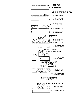
the invention was manufactured. Referring to Figures 3A to 3G, the
process for manufacturing the device structure will be explained.
At first, a YlBa2Cu30~_X oxide superconductor thin film 1 was
deposited on a STO (100} substrate 5 by MBE, as shown in Figure 3A.
The deposition condition was as follows:
Substrate Temperature: 700 °C
Deposition Atmosphere: 5 x IO-5 Ton (6.665 x IO-3 Pa; 03}
(in the vicinity of the substrate)
Deposition Duration: 10 min.
Filin Thickness: 5 nm
Then, a protective layer of STO 50 was continuously deposited on
..
the Y~.BazCu30~_X oxide superconductor thin film 1 by MBE without
breaking the vacuum, as shown in Figure 3B. The deposition condition
was as follows:
Substrate Temperature: 500 °C
2 0 Deposition Atmosphere: 5 x 10⁻⁵ Torr (6.665 x 10⁻³ Pa; 03)
(in the vicinity of the substrate)
Deposition Duration: 3 min.
Film Thickness: 3 nm
Thereafter, a STO film 51 having a thickness of 400 manometers
2 5 was deposited on the protective layer 50 by pulsed laser deposition under
a condition equal to that of Embodiment 1, as shown in Figure 3C. A
photoresist layer 6 was formed on a portion of the STO film 50, as shown
13
CA 02212827 1997-08-13
in Figure 3D, so that the STO film 50 and the YlBa2Cu30~_x oxide
superconductor thin film 1 were etched by ion milling using Ar ions so as
to form a gate insulator 52 and a superconducting channel 10, as shown in
Figure 3E. Portions of the STO substrate 5 at the both sides of the
superconducting channel 10 were exposed by the etching.
A CeOz layer 8 was deposited at the room temperature and a
portion of the Ce02 layer on the photoresist was removed by lift-off
method so that the Ce02 layer 8 was remained on the exposed portions of
the STO substrate, as shown in Figure 3F. Finally, a gate electrode 4
i 0 having a thickness of 100 nanometers was formed of Ag by evaporation at
the room temperature, as shown in Figure 3G. Thus, the device structure
using a supereonducting thin film structure in accordance with the
invention was completed.
Superconducting properties of the lower YlBa2Cu30~_X oxide
1 5 superconductor thin film of the above device structure were measured just
after deposition, and after the device was completed. The critical
temperatures of the Y~Ba2Cu30~_x oxide superconductor thin films of the
the above device structure were 71.4 K just after deposition, and 66.7 K
after the device was completed. The drop of the critical temperature was
2 0 within.5 degrees after the device was completed.
Then, a source and a drain electrodes (not shown) were formed in
contact with the both ends of the superconducting channel 10 so that
characteristics of the device were evaluated.
Figure 4 shows the drain current-voltage characteristics of the
2 5 super-FET. The modulation factor of the superconducting current was 5
% in depletion mode and 10 % in enhancement mode.
14
CA 02212827 1997-08-13
a
Figure 5 shows a comparison of the transconduction gm as a
function of normalized operating temperature (TIT) for various device
structures. In Figure 5, the transconduction values of the above device
structure using a superconducting film structure in accordance with the
invention were indicated by white circles and the values of the other
devices were indicated by black dots, black rhombi, white squares and
black triangles. As shown in Figure 5, the device structure using a
superconducting film structure in accordance with the invention had the
best properties.
As explained above, a superconducting film structure having an
. oxide superconductor layer covered with and protected by a protective
layer ~is provided in accordance with the present invention. The
superconducting film structure in accordance with the present invention
can be favorably applied to the superconducting device in which the oxide
superconductor layer and protective layer constitute elements of the
device. In addition, when a metal layer is formed on the protective layer
and it is alloyed with the protective layer, the metal layer can be an
electrode which is electrically connected to the oxide superconductor
layer.
2 0 The invention has thus been shown and described with reference to
the specific embodiments. However, it should be noted that the present
invention is in no way limited to the details of the illustrated structures
but converts and modifications may be made within the scope of the
appenc~d claims.
2 5 The entire disclosure of Japanese Patent Application No. 8-231517
filed on August 13, 1996 including specification, claims, drawings and
summary are incorporated herein by reference in its entirety.