Note: Descriptions are shown in the official language in which they were submitted.
CA 02213017 1997-08-13
METHOD AND APPARATUS FOR CONTROLLING PROPAGATION
OF ELECTRICAL CHARGES USING MULTIPLE COHERENT
LIGHT BEAMS
FIELD OF THE INVENTION
This invention relates generally to a method and
apparatus for generating and controlling the propagation of
electrical charges, such as photoelectrons and holes, in a
semiconductor material. More particularly, the invention
relates to generating and controlling the magnitude and
direction of the current produced in a semiconductor
material from multiple laser beams by varying the phase
difference between the beams and/or the polarization of one
or more of the beams with respect to the semiconductor. In
one embodiment, the invention relates to using two or more
laser beams to control the propagation of photoelectrons in
a bulk semiconductor by varying the phase difference
between the beams, and/or, the polarization of one or more
of the beams.
BACKGROUND OF THE INVENTION
In the past, it has been known to cause a current to
flow in a semiconductor material by applying a voltage
differential across the semiconductor. Such a voltage
differential can be applied by using wires connected across
the semiconductor.
The present invention relates to generation of charge
carriers in semiconductors using optical beams irradiating
a region of the semiconductor. The charge carriers
generated in this manner form a current which has a
direction and a magnitude. The direction and magnitude of
the current is dependent upon the interference effects in
the generation process as determined by characteristics of
the optical beams, such as the relative phase difference
between the beams and the polarization of the beams.
In U.S. patent 5,459,604 in the name of Corkum and
Liu, a method and apparatus for propagating photoelectrons
CA 02213017 1997-08-13
-- 2 --
in a semiconductor material is disclosed. However, the
system and apparatus disclosed in this reference relates to
use of two beams only. This reference discloses that the
two beams must be harmonically related such that the
frequency of one beam is approximately twice the frequency
of the other beam. In addition, this reference discloses
only one manner of controlling the propagating
photoelectrons, namely by varying the phase relationship
between the two beams of light. Moreover, this reference
only discloses an apparatus comprising a specific type of
semiconductor material, namely a quantum well, which can
only be used at low temperatures such as about 80 K and
does not produce positively charged holes. In addition,
the wavelengths disclosed in this reference are in the
range of 5 to 10 microns, which is far in the infrared
range.
Accordingly, the prior art suffers from the
disadvantages that only beams being harmonically related
can be used, and that only varying the phase relationship
between the beams can be used to vary the direction of
propagation of photoelectrons. Moreover, the prior art
only discloses the use of a specific type of semiconductor
material, namely a quantum well, which must be used at
temperatures substantially below room temperature.
SUMMARY OF THE INV~;N'1'1ON
Accordingly, it is an object of this invention to at
least partially overcome the disadvantages of the prior
art. Also, it is an object of this invention to provide an
alternative type of apparatus and method to generate and
control the propagation of photoelectrons in a
semiconductor material. This type of method and apparatus
would be more versatile than the prior art in that coherent
beams which are not harmonically related could be used,
bulk semiconductors in addition to quantum wells could be
used, and polarization in addition to phase relationship
between the beams can be used to control the propagating
CA 02213017 1997-08-13
photoelectrons. In addition, this method and apparatus can
be used at room temperature using coherent light beams
having wavelengths which are generally accepted in the
industry.
Accordingly, in one of its aspects, this invention
resides in providing a method of generating and propagating
electrons in a semiconductor material, said propagating
electrons creating a current having a direction and a
magnitude, the method comprising the steps of:
simultaneously irradiating a selected region of the
semiconductor material with a first coherent light beam
having a first frequency and at least two other coherent
light beams, each beam having a frequency, wherein said
first light beam and said at least two other light beams
are related such that the first frequency substantially
equals a sum of the frequencies of the at least two other
coherent light beams, and wherein the at least two other
beams together produce substantially the same number of
electrons in the semiconductor material as the first beam.
In one embodiment, the invention relates to the use of
three coherent light beams, or laser beams, related such
that the frequency of one beam substantially equals the sum
of the frequencies of the other two beams, and, each of the
beams have an intensity such that they produce
substantially the same number of photoelectrons in the
semiconductor material.
In a further embodiment, the present invention relates
to varying a polarization of at least one of the beams to
change the direction and/or magnitude of propagation of the
photoelectrons.
In a further embodiment, the present invention relates
to use of a semiconductor material comprising gallium
arsenide at a temperature between -40~C and 100~C.
In a further aspect, the present invention provides a
method of generating and propagating electrons in a
semiconductor material, the propagating electrons creating
a current having a direction and a magnitude, the method
CA 02213017 1997-08-13
comprising the steps of: simultaneously irradiating a
selected region of the semiconductor material with a first
coherent light beam having a first frequency and a second
coherent light beam having a second frequency, wherein said
first light beam and the second light beam are related such
that the first frequency is substantially twice the second
frequency and the first beam produces substantially the
same number of electrons in the semiconductor material as
the second beam; and varying a polarization of the first
beam or the second beam relative to the semi-conductor to
change the direction and magnitude of the current.
In another aspect, the present invention provides an
apparatus for controlling propagation of electrons in a
semiconductor material comprising: coherent light source
means for providing a first coherent light beam having a
first frequency and at least two other coherent light
beams, each of the at least two other beams having a
frequency, to simultaneously irradiate a selected region of
the semiconductor material, the coherent light beams being
related such that the first frequency substantially equals
a sum of the frequencies of the at least two other coherent
light beams, and wherein each of the beams have an
amplitude such that the at least two other beams together
produce substantially the same number of electrons in the
semiconductor material as the first beam; wherein
irradiating the selected region of the semiconductor causes
electrons to propagate in the semiconductor, said
propagating electrons creating a current having a direction
and a magnitude.
Further aspects and advantages of the invention will
become apparent upon reading the following detailed
description and the drawings which illustrate the invention
and preferred embodiments of the invention.
It is understood that while the present invention will
be described generally in terms of a method and apparatus
for varying or controlling propagation of photoelectrons in
a semiconductor, the present invention can relate to any
CA 02213017 1997-08-13
type of device or method where the propagation of
photoelectrons, and electrical charges in general, need be
controlled, such as for the detection of current, or for an
application in which coherent control is used to switch
other devices or detect changes in the phase or
polarization of coherent light beams.
BRIEF DESCRIPTION OF THE DRAWINGS
In the drawings, which illustrate embodiments of the
invention:
Fig. lA is a block diagram of an apparatus according
to one embodiment of the present invention;
Fig. lB is a detail drawing showing the semiconductor
being irradiated by the laser beams;
Fig. 2 is a graph illustrating control of the
propagation of photoelectrons by varying the phase
differential between the three light beams;
Fig. 3 is a block diagram of an apparatus according to
a further embodiment of the present invention;
Fig. 4 illustrates the principles of current
generation and propagation showing valence and conduction
band carriers.
DETATTlT~n DESCRIPTION OF PREFERRED EMBODIMENTS
OF THE INVENTION
Reference is made to Fig. lA which shows an apparatus,
shown generally as 10, according to one embodiment of the
present invention. The apparatus 10 comprises a first
optical source 12 which produces a coherent light beam,
such as a laser beam. In a preferred embodiment, the first
optical source 12 is an actively mode-locked picosecond
Ti:sapphire laser operating at 800 nm with a corresponding
frequency ~1 being about 3.75x10¹⁴Hz. For convenience this
beam shall be referred to as the first beam ~1 and shall be
identified in Fig. lA by the reference symbol ~1.
The first beam ~1 synchronously pumps a KTP (potassium
titanyl phosphate)-based parametric generator 14. The
CA 02213017 1997-08-13
generator 14 produces a 1 ps signal pulses turnable near
1.5~m and 1.7~m wavelength in 1 ps signal pulses. The
1.5,um wavelength laser beam has a frequency C'~2 of 2x10¹⁴Hz,
and shall be referred to as the second beam ~')2 and
identified in Fig. lA by the reference symbol ~d2, and
likewise, the 1.7~m wavelength beam has a frequency of
about 1.76x10¹⁴Hz and shall be referred to as the third beam
(~3 and identified by the reference symbol ~3.
In the embodiment shown in Fig. lA, the parametric
generator 14 will generate the laser beams ~ z, ~3 in such
a manner that all three beams ~1~ ~2, ~3 are linearly
polarized. However, the second beam ~1~2 will be linearly
polarized in the same direction as the first beam ~1 and the
third beam C1~3 will be linearly polarized in a direction
orthogonal to the direction of the polarization of the
first beam ~1 and second beam ~2. The generator 14 can also
be used to control the relative intensities of the three
beamS ~1~ ~2~ ~3-
The three beams~ 2~ 3 are reflected by a first flat
mirror MF1 into a chopper 16. The chopper 16 is connected
to a lock-in amplifier 18. In combination, the chopper 16
and lock-in amplifier 18 average the signals produced by
the three laser beams ~1~ ~2, ~3. In addition, the lock-in
amplifier 18 measures and records the current or current
density J generated in the semiconductor 20.
After the chopper 16, the three beams ~ 2~ ~1)3 are
reflected by the second flat mirror MF2 to a third flat
mirror MF3 which is partially transparent. The third flat
mirror MF3 reflects the three beams ~ 2~ ~3 to a glass
plate 22. The glass plate 22 alters the phase relationship
between the three beams ~ 2~ ~3. The angle of incidence
of the three beams ~1~ ~2, ~3 can be changed by rotating
the glass plate 22. The difference in the phase
relationship will depend on the difference in dispersion
between the three beams ~1' w2, ~3. The phase relationship
between the three laser beams w~ 2~ ~3 will change with the
CA 02213017 1997-08-13
angle ~ in a controlled manner. The beams ~ z, ~3 are
reflected back by the fourth flat mirror MF4 to pass
through the glass plate 22 a second time. In this way,
misalignment i5 avoided and the glass plate 22 operates on
the three beams c~ 2~ ~)3 twice.
In a preferred embodiment, the glass plate 22 is a l
mm thick BK7 glass window with a l/5 wavelength surface
flatness. The glass plate 22 is mounted on a double pass
configuration so that the spatial walk-off effects vanish.
The three beams ~1~ ~z, ~3 then pass through the third
flat mirror MF3 and through a half wave plate 24. The half
wave plate 24 operates on at least one of the laser beams
~2~ ~3 to change the polarization of the beams ~ 2 ~1)3.
The half wave plate 24 can operate on any one of the three
beams c~ 2~ C')3/ as well as more than one of the beams
C')2' ~3. In this way, the polarization of the three beams ~1l
Cl)2l Ct~3 can be oriented with respect to each other and with
respect to the semiconductor 20.
In the embodiment shown in Fig. lA, the half wave
plate 24 is a 0.75 mm thick quartz half wave plate and
operates on the third beam ~3 to convert the initially
orthogonally polarized third beam ~3 to have the same linear
polarization state as the other two beams, namely the first
beam ~1 and the second beam ~2. In other words, the half
wave plate 24 changes the polarization of the third beam
(1~3 from orthogonal to the polarization of the first and
second beams ~1l ~1~21 which is how the three beams ~1l ~21 (~3
are generated by the parametric generator 14, to be
parallel to the polarization of the first and second beams
2l SO that all three beams ~ 2l ~3 are polarized in
the same way.
The three beams ~ 2~ C~)3 are then reflected by a fifth
flat mirror MF5 to a curved mirror MC. The curved mirror
MC has a focal length of 2.5 cm which focuses the three
beams ~1l (L~21 ~3 onto a selected region 26 on the
semiconductor 20. In a preferred embodiment, the curved
CA 02213017 1997-08-13
mirror MC is a gold spherical mirror which focuses the
three beams ~ 2, ~3 onto a selected region 26 which is a
lOO~m diameter spot. The selected region 26 is shown in
detail in Fig. lB. The selected region 26 of the
semiconductor 20 is simultaneously irradiated by all three
beamS ~1~ ~2~ ~3-
In the embodiment shown in Fig. lA, the three beams ~1~
~2, ~3 have an amplitude such that the first beam ~1~ which
has the highest frequency, generates substantially the same
number of electrons in the semiconductor material 20 as the
other two beams, namely the second beam ~2 and the third
beam C~3, produce together. This is accomplished in the
preferred embodiment shown in Fig. lA by the parametric
generator 14 being adjusted so that the amplitude of the
three beams ~1~ ~2~ ~1)3 iS such that the second beam ("2 and
the third beam ~3 together produce substantially the same
number of electrons in the semiconductor material 20 as the
first beam ~1. Alternately, the same effect can be obtained
by placing filters, or other attenuating devices, which
would attenuate the beams ~1~ ~1)2 " "3 such that this condition
can be satisfied.
When the selected region 26 of the semiconductor 20 is
simultaneously irradiated with the three beams ~1~ ~2' Cl~3,
electrical charges in the semiconductor 20 will be
generated and will propagate in a direction. The
propagating electrical charges will form an electrical
current having a direction and a magnitude. The electrical
charges in the semiconductor 20 comprise electrons and,
depending on the nature of the semiconductor 20, the
electrical charges can also comprise holes. The electrons
have a negative electrical charge while the holes have a
positive electrical charge. The holes generally propagate
in a direction which is opposite to the propagation of the
electrons.
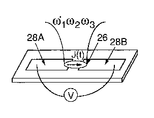
In Fig. lB, the direction of propagation of the
electrons is shown by the current density vector J(t). If
holes are also generated, the holes would have the same
CA 02213017 1997-08-13
magnitude but the opposite direction of propagation to the
electrons. In the present embodiment, the current created
by the electrons propagating in the semiconductor 20 can be
sensed by the lock-in amplifier 18.
In a preferred embodiment, the semiconductor 20 is an
electrically unbiased, planar, metal-semiconductor-metal
(MSM) device. The semiconductor is a l~m thick epilayer of
undoped GaAs grown at low temperature, about 200~C, on a
GaAs substrate with (100) orientation and is annealed for
10 minutes at 650 K. The semiconductor 20, made in this
manner, shall be referred to as LT-GaAs, and has a 2~
excess arsenic concentration which produces a high
resistivity of more than l,OOO,OOOn*cm and an electron,
hole trapping time of about 1 ps.
The use of LT-GaAs has several advantages. For
example, since electrons and holes are trapped so quickly,
deleterious effects associated with charge accumulation
during high repetition rate pulse illumination are
prevented. A short trapping time also prevents the metal-
substrate-metal configuration from acting as a capacitor
and discharging through the semiconductor since it returns
to an insulating state shortly after optical excitation.
Several pairs of 200~m by 250~m gold electrodes, shown
as 28A and 28B in Fig. lB, having an approximate thickness
of 170 nm and with gaps of 5~m to 50~m are deposited on the
LT-GaAs semiconductor 20 using photolithography. The
electrodes 28A, 28B are placed so as to have the gap
direction parallel to the (100) crystallographic axis of
the semiconductor 20.
In this configuration, the dark resistance of the 5~m
gap MSM is measured to be 13.2Mn with a capacitance of 6 pF
giving a RC rise time constant of approximately 1 ms in the
dark. For peak semiconductor radiance of 2OMW/cm2 and
3kW/cm2 at the frequencies ~1 ~')2 ~3 the optical properties
of normal GaAs and LT-GaAs do not differ significantly for
the wavelength considered. The magnitude and direction of
the electrons and holes propagating in the semiconductor 20
CA 02213017 1997-08-13
-- 10 --
can be measured by measuring the voltage or current across
the two electrodes 28A, 28B.
By irradiating the selected region 26 simultaneously
with the three beams ~ 2~ ~3~ the electrons will be
generated and will propagate in the semiconductor 20 in a
direction. The propagating electrons create a current
having a direction and a magnitude. The direction and
magnitude of the current will be dependent on the phase
relationship amongst the three beams ~1 ~2 ~')3- By varying
the phase relationship between the three beams ~1 ~2, ~3,
the direction and magnitude of the current in the
semiconductor 20 can be varied and thereby controlled.
This is illustrated in Fig. 2 which shows the voltage
measured across the semiconductor 20 by the lock-in
amplifier 18 as the relative phase between the second and
third beams ~\W2 + ~W3 with respect to the phase of the first
beam ~w1 The phase relationship ~w2 + ~w3 ~ ~w1 can be
varied by increasing or decreasing the angle ~ of the glass
plate 22. It is understood that the direction and the
magnitude of the current can be controlled by varying the
phase relationship between any of the three beams ~, ~2 and
~3-
In addition to varying the relative phase between the
three beams ~ 2 ~3~ it is also possible to vary, and
thereby control, the direction of the propagating
electrical charges, namely the electrons and/or holes, by
varying the polarization of one or more of the three beams
~1 ~2 ~3. It is thereby possible to vary, and thereby
control, the direction and/or magnitude of the current
created by the propagating electrical charges. In order to
obtain the greatest magnitude of the current in a
particular direction, all three beams ~1 ~2, ~3, are
linearly polarized and the polarization is across the gap
along the (lO0) crystallographic axis of the lattice of the
semiconductor 20. The semiconductor 20 is oriented such
that the linear polarization of the three beams ~1 ~2~ C')3 iS
across the gap along the (lO0) crystallographic axis.
CA 02213017 1997-08-13
By varying the polarization of at least one of the
beams ~1 ~2, ~3 with respect to the (lO0) crystallographic
axis, the direction and magnitude of the current in the
semiconductor 20 can be varied and thereby controlled. For
example, as shown in Fig. lA, the first and second beams ~1~
Cl)2 can be oriented such that their polarization is across
the gap along the (lO0) crystallographic axis, but the
polarization of the third beam (~13 can be varied by rotating
the half wave plate 24. By doing so, the direction and/or
magnitude of the current in the semiconductor 20 can be
changed and thereby controlled. In a similar manner, the
polarization of any one, or all, of the linearly polarized
beams ~1~ ~2~ ~3 can be varied. Likewise, any one, or all,
of the beams ~1~ 2~ (~3 can have a circular or an elliptical
polarization. By varying the polarization of any one, or
any combination of, the three beams ~ 2~ ~3, the direction
and magnitude of the current created by the propagating
charges, namely the electrons and/or holes, in the
semiconductor 20 will change in a predetermined manner, and
therefore can be controlled.
Without limiting the invention, it has been found that
the direction and magnitude of propagation of electrical
charges, namely electrons or holes, generated in a
semiconductor in the three beam embodiment, generally
satisfy the equation:
( l ) Je h = 7)e h E ~ E~2E~3 + C. C. ~Je hl'~e h
where
e,h refer to electrons and holes, respectively,
depending on which type of electrical charge is
being considered.
~-~1,E~2,E~3 are the (complex) field vector amplitudes
associated with the beams ~ 2~ ~3 in the three
CA 02213017 1997-08-13
beam embodiment.
~e,h are phenomenological current relaxation times.
J is an electrical current density vector.
J is the time rate of change of the electrical
current density vector.
~ is a material response tensor.
c.c. means complex conjugate.
It is apparent from equation (l) that changing the
polarization of one, or more, of the beams ~ 2~ C~13 will
change the propagation of the charges e, h in the
semiconductor 20 in a predictable, and therefore,
controllable manner.
In the same manner, it is apparent that additional
control of the direction and magnitude of the current in
the semiconductor 20 can be obtained by varying both the
phase relationship between the first beam ~1~ the second
beam ~2 and the third beam ~3, and, in addition, varying the
polarization of at least one of the three beams ~" ~2 and
~3-
The preferred embodiment shown in Fig. lA has been
discussed in terms of the three beams, namely the first
beam ~1 having a wavelength of 800 nm, the second beam ~z
having a wavelength of l.5um and the third beam ~3 having a
wavelength of l.7~m, such that the frequency of the first
beam ~1 substantially equals the sum of the frequency of the
second beam ~'t2 and the frequency of the third beam ~3.
However, it has been found that the same method and
apparatus lO discussed above with respect to three beams ~1
~2, ~3, can also be extended to embodiments comprising a
CA 022l30l7 l997-08-l3
- 13 -
larger number of beams provided the other characteristics
of these beams satisfy the characteristics of beams c~ 2~
~3 discussed above. In other words, if more than three
beams ~1 ~2, W3 are used, it is necessary that the frequency
of the first beam ~1 be substantially equal to a sum of the
frequencies of all of the other coherent light beams
irradiating the selected region 26 at substantially the
same time. In addition, it is necessary that the first
beam ~1 have an amplitude relative to the other beams such
that the other beams together produce substantially the
same number of electrical charges in the semiconductor
material 20 as the first beam ~1~
For example, if four beams ~1 ~2~ C~3~ 4 (not shown)
were used, it would be necessary that the frequency of the
first beam ~1 be substantially equal to a sum of the
frequencies of the other beams, namely the second beam ~2,
the third beam ~3 and the fourth beam Cl~4. Likewise, it
would be necessary that the amplitude of the second beam ~2,
the third beam ~3 and the fourth beam ~4 be such that these
beams ~2, ~3, ~4 together produce substantially the same
number of electrical charges in the semiconductor material
20 as the first beam ~1~ It is understood that in a similar
manner, the present invention will operate with five beams,
six beams, etc.
In the embodiment shown in Fig. lA, the three beams ~1
~2~ ~')3 are shown as being separate beams and do not
necessarily overlap in space and time except at the
selected region 26 where the three beams Cl~1 ~2~ 3 are
focused by the curved mirror MC. However, it is understood
that the invention could also operate if the three beams
overlapped in space and time throughout the apparatus lO
such that they occupy the same space during the same time
period from the parametric generator 14 through to the
selected region 26 of the semiconductor 20.
As described above with respect to Fig. lA, the
frequency of the second beam ~"2 can differ from the
CA 02213017 1997-08-13
frequency of the third beam Cl~3. In this way, increased
versatility is provided in that a potentially infinite
number of frequencies can be used in the three beam
embodiment, provided the sum of the frequency of the second
beam ~2 and the frequency of the third beam ~.13 substantially
equals the frequency of the first beam ~1. When embodiments
with four or more beams are considered, the invention
offers even more versatility provided the frequency of one
of the beams substantially equals the sum of the
frequencies of the other beams.
In a special or "degenerate" case, it is possible that
the frequency of the second beam~l~2 substantially equals the
frequency of the third beam ~3. In this case, the
embodiment will still operate provided that the frequency
of the first beam ~1 is equal to the frequency of the second
beam Cl~2 plus the frequency of the third beam ~1)3. In this
special case, it is possible that the third beam C~)3 and the
second beam C')2 be formed by one beam only because the
frequencies of the second beam ("2 and third beam ~3 are the
same. In other words, the frequency of the first beam ~1 is
two times the frequency of the second beam ~2.
Fig. 3 shows the apparatus for the special or
degenerate case, marked generally as 50. The apparatus 50
comprises several components which are also shown in Fig.
lA, and, like components are marked with like reference
numerals.
The apparatus 50 shown in Fig. 3 comprises an optical
source 12, which in a preferred embodiment is an actively
mode-locked picosecond Ti:sapphire laser, and is used to
synchronously pump the KTP-based parametric generator 14.
However, the generator 14 in this embodiment produces a
single 1 ps coherent pulsed beam tunable near 1500 nm, and
hereafter referred to as ~9 and identified in Fig. 3 by
reference symbol ~9. The apparatus 50 further comprises a
chopper 16 and lock-in amplifier 18, which perform a
similar function to that in Fig. lA. Apparatus 50 further
CA 02213017 1997-08-13
comprises a lens L1 with a 5 cm focal length which focuses
the beam ~9 onto a 1 mm thick BBO (~-barium borate) crystal
52 using type I phase matching which generates a second
beam (hereafter referred to as 2~9) at the second harmonic
of the first beam ~9. These beams ~9, 2~9 are focused by the
curved mirror MC1 to the flat mirror MF3 through the glass
plate 22 and half wave plate 24, to finally be focused by
curved mirror MC2 onto the semiconductor 20. The beams ~9,
2~9 overlap in space and time in Fig. 3.
The half wave plate 24 in this embodiment varies the
polarization of one of the beams relative to the gap
direction parallel to the (100) crystallographic axis. By
varying the polarization of one or both of the beams ~9,
2~9, the magnitude and/or direction of the current created
by the propagating electrical charges generated in the
semiconductor 20 can be changed in a predetermined manner
from a magnitude in any number of directions to zero where
no effect is measured. In this way, the direction and/or
magnitude of the current can be controlled without varying
the phase difference between the first beam ~9 and the
second beam 2~9. Of course, it is possible to control the
direction and/or magnitude of the current by varying both
the polarization of one or more of the beams ~9, 2~9 and the
phase difference between the beams also.
As stated above with respect to the embodiment shown
in Fig. lA, the polarization of any one of the beams ~9, 2~9
can also be varied such as by causing the beams ~9, 2~9 to
be circularly polarized or elliptically polarized. Other
manners of varying the polarization of the beams ~9, 2~9 are
also possible as are known to persons skilled in the art.
Fig. 4 illustrates theoretically how the embodiment
shown in Fig. 1 operates, however, it is understood that
the invention is not limited to this theoretical
explanation. Fig. 4 is a representation in momentum space
showing the production of the photoelectrons and the effect
described in the embodiment shown in Fig. lA. The abscissa
CA 02213017 1997-08-13
of Fig. 4 represents the momentum of the electrons and the
ordinate of Fig. 4 represents the energy of the electrons.
Fig. 4 shows the three beam embodiment where the frequency
of the first beam ~1 is substantially equal to the sum of
the frequency of the second beam C')2 and the frequency of the
third beam (1~3. As shown in Fig. 4, the first beam ~1 causes
photoelectrons to jump from the valence band to the
conduction band. The second beam (1~2 and the third beam ~3
together can also generate photoelectrons. By varying the
phase relationship between the three beams ~1~ ~2, ~3 and/or
varying the polarization of at least one of the beams ~1'
~2, ~3, it would be possible to alter the interference
between the two processes to thereby control the direction
and magnitude of the current created by the propagation of
the photoelectrons generated by the three beams c~ 2~ ~3.
It is understood that while the present invention has
been described with respect to a particular type of laser
to produce a coherent light beam, the invention is not
limited to this type of laser. Rather other types of
coherent light sources could be used. For example other
types of lasers, such as diode lasers, could be used.
It is understood that the present invention is not
temperature sensitive. In the preferred embodiment,
utilizing the LT-GaAs as the semiconductor 20, the
experiments were conducted at room temperature and the same
results could also be obtained at other temperature ranges,
such as within a temperature range of between about -40~C
and 100~C.
It will be understood that, although various features
of the invention have been described with respect to one or
another of the embodiments of the invention, the various
features and embodiments of the invention may be combined
or used in conjunction with other features and embodiments
of the invention as described and illustrated herein.
Although this disclosure has described and illustrated
certain preferred embodiments of the invention, it is to be
understood that the invention is not restricted to these
CA 02213017 1997-08-13
particular embodiments. Rather, the invention includes all
embodiments which are functional or mechanical equivalents
of the specific embodiments and features that have been
described and illustrated herein.