Note: Descriptions are shown in the official language in which they were submitted.
CA 0221308~ 1997-08-14
This invention relates to electromagnetically
operable display elements, and to a novel means of operating
and mounting them.
Such display elements are exemplified by :
anyone of those shown in :
U.S. Patents 5,050,235 Browne
RE 35,357 Browne
5,337,077 Browne
4,566,210 Winrow
5,156,872 Helwig
whose contents are incorporated herein by reference. The
devices in such patents are examples of such elements,
wherein an electromagnetic core is switched in magnetic
polarity by a coil surrounding the core. The display
element switches between OFF to ON state responsive to a
change in core polarity. In OFF state a rotor or other
moving element displays one appearance (usually dark) in
the viewing direction, and a contrasting appearance is
displayed, which is usually bright, in ON state.
For example :
Viewing Direction Viewing Direction
Patent Appearanoe in ON State Appearanoe in OFF State
5,050,235 Bright Disk Side Dark Disk Side
with LED LED shuttered
RE 35,357 Bright Disk Side Dark Disk Side
with Fibre Optic Optic is shuttered
5,337,077 Fibre Optic Optic is shuttered
4,566,210 Bright side of Bright side is
Lever hidd~-n
5,156,872 One side of Disk Contrasting Side of
Disk
131A
CA 0221308~ 1997-08-14
In each of the above examples the cores are wound with
helical colls to provide the magnetizing turns. A separate
means is provided for mounting the display elements whether
as single indicators, rectangular modules or large arrays or
other arrangements. The mounting means involves considerable
expense.
In accord with this invention an insulating board
is provided with conducting paths formed on a surface thereof
which paths act as a turn or a series of turns about a bore
in the board and hence as a turn or series of turns about a
core when a pin is inserted therethrough. The final insulating
board may be a lamination of a number of sub layers of such
boards if the number of turns requires more turns than can
be conveniently placed on one surface. The conductors are
arranged relative to an aperture for a core. The 'flat coil',
so called to differentiate it from the usual helical coils,
may be prefabricated on a surface of the insulating board or
its layers. Hence the step of winding is eliminated. A flat
coil of more than one turn will (usually) include a spiral
which need not be geometrically regular. The number of turns
about a bore on any one surface is limited by the fact that
there is a limit for spiral size at the point beyond which
the outeF turns do not have a successful magnetization effect.
Moreover the cost of a module or array is reduced
since the board may be prefabricated with an array of core
apertures which may be used to mount the cores and achieve
the arrangement of the display elements in a module or array.
The display element comprising the stator and rotor may be
mounted on the board. me cost of former ~untings for element,
module or array as encountered in the prior art is eliminated.
131A
CA 0221308~ 1997-08-14
By "board" herein is meant a relatively flat board of
(prefe~ablyl dielectric material commonly used to mount
circuits, or circuit components, and is here used to receive
the flat coils. Preferably, the board is of the same material
as those commonly used for printed circuit bo~ds ('PCB') or printed
wiring boards t'PWB') and is commonly made of fiberglass-filled
epoxy resin, although boards formed from other materials may be
used. The board as described herein is used to mount the
flat coils and the display elements in desired relationship
to the coils and to each other. 'Board' herein includes a
lamination of sub layers of thinner boards.
By 'flat coil' herein, I mean a pattern of thin
ribbon or film conductors formed on the surface of a board
layer or on sub-layers thereof to magnetize a core passing
through the board within the magnetic field of the coil. Thus,
the magnetization will be in opposite senses for opposite
current flow through the coil. A 'flat coil' includes a
series of coils surrounding a common bore but arranged on
different sub layers of the board.
Turns are defined after reference to the drawings of
the specific embodiment.
Commonly the pattern of film or ribbon is formed on
the board by covering it with attached metal foil and etching
away the portion not desired for the pattern. The foil is
usually of copper. The invention is not however dependant
on the method of forming the laminated conductor on the board.
Thus, this conducting patterns may be supplied by painting,
printing or deposit where commercially practical methods are
available. A conductor of copper or other metal may be
provided with a surface of tin or precious metals for better
electrical contact.
--3--
131A
CA 0221308~ 1997-11-14
A 'pin' is that part of a core which magnetically drives or retains the
moving member of a display element. The first three patents listed on page 1 show
display elements using two pins on the core while the latter two elements show
display elements with a single pin on the core. The pins may also act as stops for
the movable member in some display elements.
In drawings which illustrate a preferred embodiment of the invention:
Figure 1 shows a typical display element mounted on a board. The
element is in ON position,
Figure 2 shows the same view as Figure 1, except that the element is
in OFF position,
Figure 3 shows one method of mounting the display element on a
board,
Figure 4 shows another method of mounting the display element on a
board,
Figure 5 shows a conductor arrangement on a board,
Figure 5A shows an alternative shaped conductor arrangement,
Figure 6 shows an enlarged section of two conductors, connected
through a board,
Figure 7 is a section of a multi layer board,
Figure 8 is a schematic view showing the wiring on a multi layer board,
Figure 9 shows a board with core mounting bores for a part of an array,
and
Figure 10 shows a board with elements in place for part of an array.
In the drawings: the display element is exemplified by a stator
comprising: a housing 10 having mounting posts 12 and stator pins 14 and 24 madeof magnetic material
-4-
131A
CA 0221308~ 1997-08-14
forming opposite ends of a core. A rotor 17 is mounted to
pivot about an axis lS transverse to the viewing direction V.
The rotor in this embodiment rotates between an ON and OFF
position as determined by stops which may be separately
provided or may be provided as here by the ends 14E, 24E of
pins 14 and 24 respectively. me invention inf~ rotors or movable
mP~Pr~ which do not require stops.
In ON position the element displays a bright face 20
in the viewing direction and in OFF position the element
displays a dark face 22. (Figure 10)
In the element shown a magnet 16 located in the disk
which is activated, when pin end 14E is positive and pin end
24E is negative, to move to ON position; and when the pola-
rities are reversed to move to OFF position.
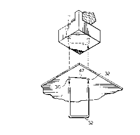
In the embodiment shown the two pins 14 and 24 are
mounted in the bores 30 and 32 respectively of Figure 3
and the element may be mounted on the cores. However, the
display element receiving the pins 14, 24, as shown, may
also be mounted on the board by separate means not shown.
The pins are connected by the integral extent 32', or may be
20 connected by a later added extent 33 (Figure 4) and may be
inserted from the top.
(Another display element such as those exemplified
on page l would provide analogous features to those described).
In accord with the invention a board 35, preferably
of fiber glass filled epoxy resin, is provided with bore
pairs 30, 32 (Fig.s) which correspond to positions for the display
element, as indicated in dotted squares 34 on Figure 9
(where the current paths are omitted), to make the array
partially shown in Figure 10 (With a differently shaped or
--5--
131A
CA 0221308~ 1997-11-14
dimensional display element shape of the areas or sizes of the elements on the
board will of course be different).
The stators may be mounted by pushing the pins 14, 24 on the U
shaped member through the board, and the pins may be attached to the housing andto the board by friction or adhesive. Preferably the pins of the U shaped member are
sliding fit with the board bores and a press fit with bores (not shown) in the housing,
to thus mount the stators on the board.
Alternatively, the pins may be attached to the board as separate
members and provided with a bridging member to form the core.
The pin lengths will normally be of sufficiently hard magnetic material
so that their magnetic polarity is retained after an energizing pulse.
Figure 8 shows in exploded view means for combining board into a
laminate board to provide more windings associated with a given core bore 30 with
extents 30A, 30B, 30C in a section of the multi layer board with sub layers A, B,C as
shown in Figure 7.
As shown, the current (pulse) supply may be brought on a foil
conductor 41A to the clockwise inward spiral 43A on board sub layer A to provide a
clockwise current flow about a core 14 in bore extent 30A. To add to the turns for a
core in bore 30A, 30B may be provided in sub layer B above or below (here below)A. Although the current paths have an insulating coating 49 (Figure 6) which avoids
shorting with paths 47 on
-6-
131A
CA 02213085 1997-08-14
a facing layer of the adjacent board, it is presently preferred
to have a board sub layer between each conductive path.
~ccordingly~ on board sub layer A, the inner end of the spiral is attached
to a connector 46A which is preferably a plated bore known as a 'via hole',
extending through the board to a position on board sub layer B having the
same azimuthal relationship to its aperture 30B as the pin's relation to the
aperture 30~ on layer A. In Figure 8 the flat ribbon shape
of the conducting path is omitted.
For addition of the magnetizing field on sub layer A
to sub layer B, layer B must also provide a clockwise spiral
path about bore 30B to the current in the direction shown.
At the outward end of the layer B spiral the conductor is
attached to connector 46B, preferably a via hole, passing through layer B
for attachment in the same azimuth positian to the outer end of the
spiral on layer C.
Thus board C may provide a clockwi~e inward spiral for
addition to turns of the coil of layer C to those of A and B.
Since the layer C spiral has clockwise inward and
clockwise downward spiral, it will be obvious that it
represents a repeat of the layer A cycle so that the drawing
represents 1 1/2 stages. Thus the stages may be continued
and the number of turns as desired accumulated as required.
~ ith the flat coils on the various sub layers
connected in series the magnetization effects in -the various
sub-layers may be added if the sub layers are arranged so that
current in the series connected flat coils travels in the
same sense (i.e. clockwise or counter-clockwise) about the
core, independently of whether an individual coil spirals in
or out.
131A
CA 0221308~ 1997-08-14
Thus current flow in one direction through the series
connected coils will create a North Pole at the pin end 14E
in the display element housing while current flow in the
opposite direction will create a South Pole at pin 14E
If the display element requires two drive pins (as
in the display element of Figure 1 and the first three patents
on page 1), the coils arranged on the board layers surrounding
the bore 32 will create the opposite magnetism to pin end 24E
~o the pin end 14E in bore 30.
Thus the sense of the turns is the same for the coils
about the pin 24 which may be threaded through aligned sub
layers if they exist. Thus, the layers shown will have
analogously connected spirals about aligned bores as in
Figure 1 but directed for current f low in the opposite
direction for the other pin 24. The winding current directions
discussed are those for one of the ON or OFF positions of the
display element. For the other of the ON or OFF positions
the current direction will of course be reversed.
On Figure 5 a foil conductor 41A leads into the
clockwise inward spiral 43D where it conducts current in a
clockwise looking downward spiral about bore 32 and a pin 24
not here shown, located herein. At the inward end of the
spiral the foil conductor is connected to connector 46A which
extends through the board 35 to the foil connector 47 on the
bottom of board 35. At the left hand end of connector 47 the
connector 47 is connected over connector 45B to the foil path41B
of counterclockwise outward of spiral 43E where with foil
path 41A it goes to the voltage or current source.
It will be seen that the coils are arranged and
connected so that current in the direction of the arrows
--8--
131A
CA 0221308S 1997-08-14
shown will magnetize the pin in bore 30 in one sense and the
pin in bore 32 in the opposite sense. Thus, if the current
in the foil paths is reversed, both pins will be switched to
opposite polarity but will still be opposite polarity to
each other.
It will be noted that if the spiral flat coils 43E
and/or 43D are replaced by series connected coils as shown
in Figure 8, that these series connected coils will be
respectively connected to the voltage source at one end and
at the other end to the connector 47.
Figure 6 shows an enlarged somewhat schematic view of
the foil paths 41A and 47 connected by cormector 45A, preferably a via hole,
tl,ro~gh the thickness of board 35.
The flat coils are, as stated insulated but their
innermost extents are set back from the bores 30 or 32 to
avoid the risk of shorting the coils.
The flat coils are considered as approximately
arranged in a plane corresponding to the median plane of the
board whether arranged as a single board surface or in series
of coils on a plurality of sub layers.
The invention has potential use for all applications
wherein a coil is presently used to magnetize a core to
'set', 'reset', or switch a display element. Other features
of a typical display element may be added to the arrangement
shown without change or at least without undue modification.
Illustrating this ~y reference to the exemplary patents
listed on page 1 : with reference to Patent 5,050,235 the,
arrangement shown may replace the wound coil with the flat
coils for an element provided with LEDs to augment the 'ON'
_g_
13LA
CA 0221308~ 1997-08-14
appearance. Similarly the inventive arrangement will acc~date
fibre optics as shown in Patents RE35,357 or 5,337,077 where a
fibre is combined with a disk or a shutter, of Patent 4,566,210
where a single pin may be energized by flat coils arranged about
a single bore where the core drives the bright face of a lever
between exposed and occluded position.
Patent 5,156,872 exemplifies a disk operated element
using a single pin. For use with the flat winding each space
on a board corresponding to a display element would have a single
core-hole and flat winding.
"Turns" herein will be defined in accord with the
following discussion. The current carrying turns shown herein
form the turns of those ampere turns which magnetize the cores
and pins herein. Such turns to be effective must be within an
effective distance to effect the desired magnetization. The
diagrams are not quantitatively accurate but in terms of a turn
approximating a 360~ travel about the magnetic core, the coil
of Figure 5 would represent two turns plus a fraction for the
straight outer patio and each layer of Figure 8 would approximate
3 1/2 turns.
A straight conductor running perpendicular to a
conductor and in proximity thereto approximates 1/2 a turn.
The shape of the spiral or coil may be a spiral with
continuously curving paths or a series of straight legs which
may be square, hexagonal, octagonal or other shape. Figure 5A
shows a spiral turn made of eight straight legs which may be
considered a spiral of octagonal form. The coil may generally
be defined by any shaped paths wnLcn provide turns within the
proper proximity to the core.
--10--
131A