Language selection

Search

Patent 2213611 Summary

Third-party information liability

Some of the information on this Web page has been provided by external sources. The Government of Canada is not responsible for the accuracy, reliability or currency of the information supplied by external sources. Users wishing to rely upon this information should consult directly with the source of the information. Content provided by external sources is not subject to official languages, privacy and accessibility requirements.

Claims and Abstract availability

Any discrepancies in the text and image of the Claims and Abstract are due to differing posting times. Text of the Claims and Abstract are posted:

  • At the time the application is open to public inspection;
  • At the time of issue of the patent (grant).
(12) Patent Application: (11) CA 2213611
(54) English Title: EMITTER BALLAST BYPASS FOR RADIO FREQUENCY POWER TRANSISTORS
(54) French Title: CONTOURNEMENT DES RESISTANCES DE PROTECTION D'EMETTEUR POUR TRANSISTORS DE PUISSANCE HAUTE FREQUENCE
Status: Dead
Bibliographic Data
(51) International Patent Classification (IPC):
  • H01L 27/06 (2006.01)
  • H01L 29/73 (2006.01)
  • H03F 3/189 (2006.01)
  • H03F 3/24 (2006.01)
(72) Inventors :
  • JOHANSSON, TED (Sweden)
  • LEIGHTON, LARRY (United States of America)
(73) Owners :
  • TELEFONAKTIEBOLAGET LM ERICSSON (Not Available)
(71) Applicants :
  • TELEFONAKTIEBOLAGET LM ERICSSON (Sweden)
(74) Agent: MARKS & CLERK
(74) Associate agent:
(45) Issued:
(86) PCT Filing Date: 1996-02-16
(87) Open to Public Inspection: 1996-08-29
Availability of licence: N/A
(25) Language of filing: English

Patent Cooperation Treaty (PCT): Yes
(86) PCT Filing Number: PCT/SE1996/000213
(87) International Publication Number: WO1996/026548
(85) National Entry: 1997-08-22

(30) Application Priority Data:
Application No. Country/Territory Date
08/393,683 United States of America 1995-02-24

Abstracts

English Abstract


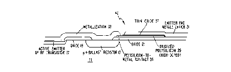
An apparatus and method are provided for bypassing the emitter ballast
resistors of a power transistor, thereby increasing transistor gain. In a
power transistor of the interdigitated type, bypassing the emitter ballast
resistors requires bypassing each individual ballast resistor with a capacitor
in parallel. Bypassing is therefore done on the silicon chip. More
particularly, in accordance with one embodiment of the invention, an RF power
transistor includes a silicon die, an emitter ballast resistor (13) formed on
the silicon die, and a bypass capacitor (40) formed on the silicon die and
connected in parallel with the emitter ballast resistor (13). The resistor may
be a diffused resistor, and the capacitor may be a metal-on-polysilicon
capacitor. In accordance with another embodiment of the invention, a method is
provided for increasing the gain of an RF transistor formed on a silicon chip
and having an emitter ballast resistor formed on the silicon chip, in which a
capacitor is formed on the silicon chip and connected in parallel with the
ballast resistor.


French Abstract

La présente invention concerne un dispositif et un procédé permettant de contourner les résistances de protection de l'émetteur d'un transistor de puissance, ce qui augmente son gain. Dans le cas d'un transistor de puissance du type interdigité, le contournement des résistances de protection de l'émetteur exige le contournement de chaque résistance de protection au moyen d'un condensateur monté en parallèle. C'est pourquoi le contournement se fait sur la puce de silicium. Plus particulièrement, selon un mode de réalisation de l'invention, un transistor de puissance HF comprend une puce de silicium, une résistance (13) de protection de l'émetteur formée sur la puce de silicium et un condensateur de contournement (40) formé sur la puce de silicium et relié en parallèle à la résistance (13) de protection de l'émetteur. La résistance peut être réalisée par diffusion et le condensateur peut être un condensateur du type métal sur polysilicium. Selon un autre mode de réalisation de l'invention, on met en oeuvre un procédé visant à augmenter le gain d'un transistor HF formé sur une puce de silicium et ayant une résistance de protection de l'émetteur également formée sur la puce de silicium, ce transistor comportant un condensateur formé sur la puce de silicium et relié en parallèle à la résistance de protection.

Claims

Note: Claims are shown in the official language in which they were submitted.


- 8 -
Claims:

1. An RF power transistor comprising:
a silicon die;
an interdigitated electrode formed on the silicon die having a
plurality of parallel electrode fingers;
diffusion regions formed beneath said electrode fingers;
a resistor formed on the silicon die and connected in series with
said electrode fingers at a first node;
a metallized region, including a bond pad area, formed on the
silicon die;
a metal path connected to said metallized region and connected to
said resistor at a second node;
a conductive layer underlying said metallized region and
connected to said electrode fingers at said first node; and
an insulating layer separating said metallized region and said
conductive layer.

2. The apparatus of Claim 1, wherein said conductive layer is doped
polysilicon.

3. The apparatus of Claim 2, wherein said insulating layer is an oxide
layer.

4. An RF power transistor comprising:
a silicon die;
an emitter ballast resistor formed on said silicon die; and
a bypass capacitor formed on said silicon die and connected in
parallel with said emitter ballast resistor.

5. The apparatus of Claim 4, wherein said emitter ballast resistor is a
diffused resistor.

- 9 -
6. The apparatus of Claim 5, wherein said capacitor is a
metal-on-polysilicon capacitor.

7. A method of increasing the gain of an RF transistor formed on a
silicon chip and having an emitter ballast resistor formed on the silicon chip,
comprising the steps of:
forming a capacitor on the silicon chip; and
connecting the capacitor in parallel with the ballast resistor.

8. A method of increasing the gain of an RF transistor formed on a
silicon chip and having a plurality of emitter ballast resistors formed on the
silicon chip, comprising the steps of:
forming a capacitor on the silicon chip; and
connecting the capacitor in parallel with each of the ballast
resistor individually.

Description

Note: Descriptions are shown in the official language in which they were submitted.


CA 02213611 1997-08-22

W O 96/26548 PCT/SE96/00213

E~L1 1'~;~C BALLAST BYPASS FOR RADIO FREQUENCY
POWER TRANSISTORS
1. Field of the Invention
The present invention relates to power transistors, more-particularly to
radio frequency (RF) power Lld~ ol.. of the silicon bipolar type. Such
L~ o-~. are cr~mmonly used in amplification stages for radio base station
S amplifiers, but are also widely used in other RF-related applir~ti-n~.
2. State of the Art
The majority of modern-day RF bipolar power ~ contain a large
~ulllber of paralleled l~ lur segmPnt~ to give a high power capacity by
distributing a large amount of current, reclnring parasitics and providing heat
10 spreading. The most common layout scheme, the inter~ligit~tprl layout, consists
of ~lle".itli.~g fingers of base and emitter regions in parallel, connPcte~l by
ribbons of mPt~lli7~tion on top of the silicon.
Active bipolar tr~n~i~tors have a positive tc~ La~u.c coeffiriPnt That
is to say, as the Lell.~e~dLulc increases, the quiescent collector current increases.
15 This condition occurs becduse the base-to-emitter voltage Vbe for a specifiedcurrent decreases at a rate of apprs~im~tely 0.002 volts per degree C. If the
bias supply of the Lld~ ol is held col~Li~L and tclllp~ldLuie increases, then
Vbe de~;-,ases and collector current i~crcases. This ill~;lcase in collector
current causes a further hlc.case in power t~ iration, which in turn causes the
20 tr~n~i~tor junction klll~cldlulc to increase even further. If there is no other
infhlPnre7 this condition causes the l.,...~;~lur to go into "thPrm~l run away"
wherein a current is reached at which the transistor fails.
There are a number of dirr~.e.lL ways to ext~rn~lly control this
condition. The most common way is a circuit which senses the collector
25 current and provides negative fee(ih~el~ to hold the collector current constant
with changes in L~ eldLulc. Another way is to use a temperature sensitive
component in the bias llCLwol~ with a k~y~eldLul~ char~rtPri~tic the opposite ofVbe. A third method is to use an emitter resistor to ground. As collector
current ill~lcascs, Vbe is re~-~re-i, and thclcrulc the base current is re~ re~

CA 02213611 1997-08-22

W 096/26548 PCT/~h9GJ'~213


Any current ext~orn~l to the ~ Lul itself adds complexity and
increases the cost of the cil~;uiLly. The most cost-errt;~;~ive method of applying
temperature compensation is the emitter-to-ground resistor. Although this
method can be quite err~cLiv~ with respect to comp~ l;.. g for changes in ~1
5 ambient LeLu~eldlule, it is quite ~lifflrlllt to locate this resistor physically close
enough to the LldL~i~Lol to ~~-i--i---i,~ emitter lead in~lllct~nre~
S~Luicc~ ol m~nllf~rtllrers have learned that the best place to locate
the emitter l~s~lol is on the silicon chip along with the active tr~n~i~tor. In
this lLIaL~" the in-l~lrt~nre in series with the emitter resistor is kept to a
0 mi~ In the seLuico~lllllrtQr i~du~Lly, this emitter resistor is often referred
to as the emitter ballast resistor, or just ballast resistor. In general, higherpower density requires higher values of emitter ballast resi.ct~nre.
Emitter ballast l~ e, re, has a lle~ iv~ effect on power gain.
Higher power gain is more desirable, as less input power is required for the
15 same ;~l~Ull~ of output power.
Typically, the intrin~jc emitter lrs;~ ..re of a bipolar L,~sisLor will be
negligible colLIp~d to the emitter ballast reci~t~nre, such that the emitter
~c~ re can be considered for practical purposes to be equal to the emitter
ballast 1~ e alone. Using a simplified transistor model, the power gain of
20 a bipolar l-, --~i~lor is given by the following equation:

Gain (dB) = 10 log ,l~ L

where ,B is the ratio of collector current to base current, RL is the collector load
re~ and re is the emitter resi~t~nre. The foregoing model does not
include higher frequency effects such as emitter lead in~l~lct~nre and does not
include the possible lleg~ive effects of collector fee~lb~rl~ capacitance on power
25 gain. Even so, it has been flrlr~ rl empirically that in general, lower re
results in higher gain. In particular, under the fol~:going model, each time re is
reduced by 1/2, gain is i,l~l~ased by 3 dB.

CA 02213611 1997-08-22

W 096/26548 PCTI~G,!~~213
-- 3 --
A common technique used in circuit design to negate the effects of re on
gain is to bypass re with a capacitor. If the capacitor has a capacitive re~ct~nre
equal to the value of re, then the total impedance of re in parallel with the
c~r~rit~r is reduced by 1/2. In this case, the bipolar Llal~iSLul can be more
S ac-;ulaL~ly modelled as follows:

RL
Gain (dB) = 10 log ~ ((r + Xc)l(re-xc))

As demonstrated by the foregoing obsel~Lions, the negative effects on
gain of the emitter ballast resistors can be o~ercu,llc by bypassing the emitterballast lCsi~ . What is neerle(l, then, is a technique for bypassing the emitterballast resistors in a power transistor of the type described.

SUMMARY OF THE INVENTION
The present invention, generally speaking, provides an a~alaLus and
m~thnf1 for bypassing the emitter ballast lc~ iL~ of a power transistor, thereby
increasing Lld~i~Lor gain. In a power Lld~iSLOl of the inter~ligit~tt-cl type,
bypas~mg the emitter ballast resistors requires bypassing each individual ballast
15 resistor with a c~p~ritQr in parallel. Bypassing is therefore done on the silicon
chip. More particularly, in accordance with one embodiment of the invention,
an RF power transistor inr~ es a silicon die, an emitter ballast resistor formedon the silicon die, and a bypass c~p~rit-7r formed on the silicon die and
cnnn~octed in p~r~llel with the emitter ballast resistor. In accordance with
20 another embodiment of the invention, an RF power transistor includes a silicon
die, and an inter~ligit~te~l electrode formed on the silicon die having a plurality
of parallel electrode fingers. Diffusion regions are formed beneath the
electrode fingers. A resistor is formed on the silicon die and is conn.-cte~l inseries with the electrode fingers at a first node. A mlot~lli7f~rl region, including
25 a bond pad area, is formed on the silicon die and is cnnn.oct~ by a metal path
to the resistor at a second node. A conductive layer nn~lerli~os the mPt~lli7~
region and is connected to the electrode fingers at the first node. An jnclll~ting

CA 02213611 1997-08-22
W 096t26548 PCT/SE96/00213


layer sepdldl~s the mf~t~ i7r~1 region and the conductive layer. In accordance
with still another embodiment of the invention, a method is provided for
i~credsillg the gain of an RF Lld~ r formed on a silicon chip and having an r
emitter ballast resistor formed on the silicon chip, in which a capacitor is
S formed on the silicon chip and conn~octed in parallel with the ballast resistor.

BRIEF DESCRIPTION OF THE DRAWING
The present invention may be further understood from the following
description in co,ljun~;lion with the appended drawing. In the drawing:
Figure 1 is a sectic)n~l view of a conventional emitter ballast resistor in a
bipolar power l~dl~ lol,
Figure 2 is a sectional view of an emitter ballast resistor including an
MOS bypass capacitor structure;
Figure 3 is a diagram of an equivalent circuit of the MOS capacitor
structure of Figure 2;
Figure 4 is a sectional view of a polysilicon/oxide/metal MOS capacitor
structure, shown integrated into a typical RF power ~n.cictor structure;
Figure 5 is a ~l-ot~ilPd plan view of a layout for a bypass c~p~ritQr in an
RF power Lldl~iSlOl, in accordance with an embodiment of the present
invention; and
Figure 6 is a diagram of an equivalent circuit of the MOS capacitor
~lluelul~ of Figure 5.

DETAILED DESCRIPTION OF THE PREFERRED EMBODIMENTS
In order to capacitively bypass the emitter ballast resistors of a power
Lld~ ol, a method of implementin~ a c~p~rit~r of high enough value to be
cipnifir~nt is required. The MOS capacitor is the most commonly used in
bipolar technology because the c~p~r-itQr is extremely linear, has a high
breakdown voltage, has a low Lclll~cldLurc coefficient, and can be fabricated
with good co~ ry of capacitance from tr~n~Cictor to transistor.
Reverse-biased PN jllnrtiC,nc can also be used, provided that the junction is

CA 02213611 1997-08-22
W 096/26548 PCT/SE96/00213


always kept reverse-biased. However, large capacitance values require high
doping levels, which lead to unacceptable breakdown voltages of the resnlting
structures.
,~ Referring to Figure 1, an emitter ballast resistor is formed (as in a
conventional bipolar power tran~Cictor) by providing in an N-type substrate 11 aP-type diffusion region 13, conn~oct~l at one end by a metal wire 15 to an
emitter finger pair and conn~ctrd at the other end by a metal wire 17 to an
emitter bond pad (not shown). The metal wire 15 and the metal wire 17
(formed in the same m~talli7~tion layer) are isolated from the substrate 11 by
portions (19 and 21, respectively) of an oxide layer.
Rer~ g to Figure 2, the simplest way, in bipolar technology, to
additionally provide an MOS capacitor is to insert in the process an additional
mask step so as to define a region above the diffusion region 13 in which a thinlayer of silicon dioxide 23 is grown. Metalli7~tion 25 is then placed over the
thin oxide layer, producing a high-value, high-breakdown voltage capacitor.
However, as shown in Figure 3, a considerable parasitic c~r~rit~nre is
present between the diffusion region 13 and the snbstrate region 11 (the
lQl FS colkctor) due to the depletion capacitance of the jnnrti~n In
other words, the diffusion region 13 becomes one plate of a parasitic capacitor,and the substrate 11 becomes an opposite plate. The c~r~rhanre occupies the
depletion region of the P/N junction, located at the interface between the
diffusion region and the substrate. Such a p~racitir capacitance is
disadvantageous it i~ lcases collector-to-emitter c~r2ritanre and because it
decreases the bandwidth of the amplifier in which the L,d~,i~,lol is used.
One way of 1O~Li11g this parasitic capacitance is to use a
polysilicon/oxide/metal c~p~cit~r. R~rt:..ing to Figure 4, the N-type substrate
11, the P-type diffusion region 13 fo..llillg a p+ ballast resistor, and the oxide
regions l9 and 21 are the same as in the conventional ~ ,ent of Figure 1.
Also shown is an active emitter region 27 of an RF ~ l al~ )l . In contrast to
30 the MOS c~ra~itQr of Figure 2, a layer of highly doped polysilicon 29 is usedto form the lower electrode of the c~r~rit~r, and is isolated from the substrate

CA 02213611 1997-08-22
W 096/26548 PCT/SE96/00213


by the oxide region 21, which can be made several microns thick. As a result,
the c~ ...re to the substrate is greatly rednred A thin oxide layer 37 is
grown above the polysilicon layer 29 and forms a dielectric betw~ell the r
c~racitrJr plates (the polysilicon layer 29, and the emitter pad m~t~lli7~tion 31).
A m~t~lli7~tion 33 co~ r~ a pair of emitter fingers to the ballast l~si~ 13
and also co ~ , the ballast resistor 13 to the polysilicon layer 29.
The rp~nltin~ polysilicon-to-metal capacitor 40 of Figure 4 is an MOS
c~p~citor having similar ~lu~L~es as the c~ ol of Figure 2.0nly standard
silicon proce~ing steps are required to add the capacitor as shown in Figure 4
into a typical high-frequency transistor process, inrln-ling one or two additional
mask steps. The polysilicon layer 29 should be heavily doped to ~
depletion effects in the c~paritor electrode. That is, if the polysilicon is notheavily doped, the polysilicon may be depleted of carriers at certain voltage
biases, ç~n~in~ c~ re in series with the oxide capacitance. This depletion
leads to a luw~ g of the total capacitance and a voltage-dependent, very
non-linear, c~ l ~ci~ re value.
A simplified detail of a typical layout for the bypass c~p~ritr,r 40 is
shown in Figure 5, here shown having only four e,l,itt~l~, (33, 34, 36 and 38)
connrcted to one bond pad 41. An actual tr~n.~i~tor can consist of several
hundred ~llPiLlt;l, connrcte(l to a bond pad. Line IV-IV in-iir~trs the cross
section shown in Figure 4. As co",~al~d to a coll~/ellLional layout, the layout
has been e-,rtrn~lr~l by adding a metal-on-polysilicon area 29, forming the MOS
capacitor 40. The c~p~ritor 40 will typically exhibit c~parit~nre values up to
lfF/um2.
The width of the metal-on-polysilicon capa.;itor 40 in Figure 5 will
depend on the c~p~rit~nre value required. For example, if 50 pF is needed for
a 1560 emitter finger layout to achieve an impedance of 1.6 Ohm at 2 GHz,
tnen the width of the metal-on-polysilicon capacitor shown in Figure 5 only
needs to be 37 um wide, if 300 A silicon dioxide on top of the polysilicon is
used. The increased size of the layout should be colllp~:d to a typical emitter

CA 02213611 1997-08-22
W 096/26S48 PCT/~h9G,'~213


finger (1;II~F .~;011 of 40-60 um and a ty-pical bond pad size of up to 100 x 100
um.
The equivalent circuit of the layout is shown in Figure 6, in which an
~I RF power ~ or 50 is conn~ct~l to a ballast resistor 13~ bypassed by a
S bypass c~p~e;lol 40~.
It will be a~lccialcd by those of orl~uy skill in the art that the
invention can be embodied in other specific forms without departing from the
spirit or ee~e..l;~l chdldch,. thereof. The ~lcscLlLly disclosed emborlim~ont~ are
Lh~.crul~ considered in all respects to be illu~,LldLive and not restrictive. The
10 scope of the invention is iiUlir,-lr(l by the appended claims Mther than the
fol~goi~, description, and all changes which come within the m.o~ning and
range of equivalents thereof are int~ntlPd to be embraced therein.

Representative Drawing
A single figure which represents the drawing illustrating the invention.
Administrative Status

For a clearer understanding of the status of the application/patent presented on this page, the site Disclaimer , as well as the definitions for Patent , Administrative Status , Maintenance Fee  and Payment History  should be consulted.

Administrative Status

Title Date
Forecasted Issue Date Unavailable
(86) PCT Filing Date 1996-02-16
(87) PCT Publication Date 1996-08-29
(85) National Entry 1997-08-22
Dead Application 2004-02-16

Abandonment History

Abandonment Date Reason Reinstatement Date
1998-02-16 FAILURE TO PAY APPLICATION MAINTENANCE FEE 1998-02-09
2003-02-17 FAILURE TO PAY APPLICATION MAINTENANCE FEE
2003-02-17 FAILURE TO REQUEST EXAMINATION

Payment History

Fee Type Anniversary Year Due Date Amount Paid Paid Date
Registration of a document - section 124 $100.00 1997-08-22
Application Fee $300.00 1997-08-22
Maintenance Fee - Application - New Act 2 1998-02-16 $100.00 1998-02-09
Reinstatement: Failure to Pay Application Maintenance Fees $200.00 1998-08-31
Maintenance Fee - Application - New Act 3 1999-02-16 $100.00 1999-02-09
Maintenance Fee - Application - New Act 4 2000-02-16 $100.00 2000-02-07
Maintenance Fee - Application - New Act 5 2001-02-16 $150.00 2001-02-07
Maintenance Fee - Application - New Act 6 2002-02-18 $150.00 2002-02-08
Owners on Record

Note: Records showing the ownership history in alphabetical order.

Current Owners on Record
TELEFONAKTIEBOLAGET LM ERICSSON
Past Owners on Record
JOHANSSON, TED
LEIGHTON, LARRY
Past Owners that do not appear in the "Owners on Record" listing will appear in other documentation within the application.
Documents

To view selected files, please enter reCAPTCHA code :


To view images, click a link in the Document Description column. To download the documents, select one or more checkboxes in the first column and then click the "Download Selected in PDF format (Zip Archive)" or the "Download Selected as Single PDF" button.

List of published and non-published patent-specific documents on the CPD .

If you have any difficulty accessing content, you can call the Client Service Centre at 1-866-997-1936 or send them an e-mail at CIPO Client Service Centre.


Document
Description 
Date
(yyyy-mm-dd) 
Number of pages   Size of Image (KB) 
Abstract 1997-08-22 1 58
Description 1997-08-22 7 305
Representative Drawing 1998-01-07 1 5
Claims 1997-08-22 2 45
Drawings 1997-08-22 2 37
Cover Page 1998-01-07 1 64
Claims 1997-08-23 2 56
Fees 1998-08-31 2 86
Correspondence 1998-06-16 3 65
Correspondence 1998-07-31 1 1
Correspondence 1998-07-31 1 2
Assignment 1997-08-22 7 321
PCT 1997-08-22 8 286
Prosecution-Amendment 1997-08-22 3 79
Correspondence 1998-04-01 1 17