Note: Descriptions are shown in the official language in which they were submitted.
~ CA 02213855 1997-08-26
RTO 96128885 PCTIUS96/02983
-1-
SLOPE, DRIFT AND OFFSET COMPENSATION IN ZERO-IF RECEIVFR~
The present invention relates to radio receivers and more particularly to
compensating radio :receivers that are a special case of superheterodyne
receivers
having an intermediate frequency of zero.
BACKGROU1~1D OI~ THE DISCLOSIJKEE
In the field of radio receivers, there has been a concentrated effort to
reduce
the amount of tuned circuitry used in the receivers. By reducing the number of
tuned
circuits, Iarge portions of the receiver can be integrated resulting in
smaller receivers.
These compaca receivers can then be used in many areas such as cellular
telephones.
A major advance in the design of such receivers is a technique known as the
"zero-
IF" technique..
According to theory, an IQ radio receiver can be constructed according to
Figure i, in vvhich the radio signal S from the antenna 1 is applied directly
to two
balanced, quadrature mixers 2a, 2b (mathematically-multiplying devices) where
the
signal is multiiplied respectively by a sine and cosine wave at the carrier
frequency of
signal S generated by a Iocal oscillator 3. In this manner, the I-channel or
in-phase
signal and the. Q-channel or quadrature signal are generated. The
multiplication
devices yield outputs containing both sum frequency components around 2f and
difference fre~~uency components around zero frequency. DC or low pass filters
4a,
4b eliminate the former and accept the latter. The zero frequency components
can
then be amplified to any convenient level by low-frequency amplifying stages
Sa, Sb
instead of high frequency amplifiers. Essentially, the zero-IF receiver
eliminates the
interim conversion to an intermediate frequency by converting the incoming
signal
directly to ba~eband in a single operation.
In practice, this so-called zero-IF approach is beset with a variety of
practical
problems, one of which concerns the imperfection of the balanced mixers as
compared '
to perfect malihema6cal multipliers. The most troublesome aspect of this
imperfection
is the generation of a DC offset or standing voltage that can be many orders
of
CA 02213855 1997-08-26
WO 96/28885 PCT/US96/02983
-2-
magnitude greater than the desired signal. The low frequency amplifiers, which
receive the mixer outputs, can be forced into saturation by the large DC
offset long
before the desired signal has been amplified sufficiently.
To avoid premature saturation, RF amplifers can be added ahead of the mixers
to raise the desired signal voltage level. Unfortunately, a common source of
the
offset is leakage from the local sinusoidal oscillator back to the antenna,
producing
coherent inteWerence. As a result, RF amplification is not a satisfactory
solution
because the desired signal and coherent interference are amplified equally.
Another proposed solution used in conventional superheterodyne radio
receivers is partial amplification of the input signal at the original antenna
frequency.
The partially amplified signal is then converted to a convenient intermediate
frequency
IF for further amplification before being applied to the balanced quadrature
mixers.
In this situation, the locally generated sine and cosine waves are at the IF
rather than
the antenna frequency, so leakage back to the antenna is of no consequence.
However, by adding IF tuning circuitry, the simplicity and reduced size of the
zero-IF
receiver are lost. An alternative method of overcoming DC offset from the IQ
mixers
may employ the technique variously called AC coupling, DC blocking, high-pass
filtering or differentiation to eliminate the standing or DC offset voltage.
The trade-
off with this method is the result that the DC and low-frequency components
are lost
or gravely distorted. This trade-off is unacceptable in digital transmission
systems
which use QP~SK (Quadrature Phase Shift Keying) or MSK (Minimum Shift Keying)
modulation techniques. These modulation techniques generate low frequency
components that must be preserved.
U.S. F~atent No. 5,241,702 discloses a method of compensating for low
frequency offset without losing or distorting the DC and low-frequency
components of
the desired sil;nal. Initially, the received signal is differentiated to
filter out the DC
offset. The signal is amplified to a suitable level and then integrated to
recapture the
original DC and low frequency signal components. The integration essentially
restores the filtered components to their original values in the amplified
signal using
an arbitrary G~nstant of integration of bounded magnitude to generate a
restored
signal. Using various techniques that exploit predetermined signal patterns or
inherent
CA 02213855 2004-11-12
-3-
signal properties of the desired signal, the DC offset estimate is then
subtracted out of the
restored signal leaving the amplified, received signal substantially free from
distortion. A
preferred way of removing such unwanted DC offsets by means of digitizing the
time
derivatives of the I and Q waveforms will now be described. After digitizing
the derivatives,
the digital values arc re-integrated in an I and a Q accumulator to restore
tile I,Q values.
The re-integration process introduces arbitrary constants of integration into
the I and Q values
which are now however of comparable magnitude to the wanted signal and can be
estimated
and removed according to the aforementioned pateat. Errors in the digitizing
process can
lead additionally to the re-integrated I and Q values exhibiting a systenzstic
increase or
decrease, and this unwaated slope is now removed at the same time as ranoving
the
unwanted arbitrary constants of ro-integratyon by estimating both the
constants and the slopes
and subtracting these systematic errors from the I and Q waveforms
respectively, The I and
Q waveforms are then processed by numerical signal processing algorithms to
demodulate
and decode the information.
"A New Approach to Eliminate the DC Offset in a TDMA Direct Conversion
Receiver" by B. Lundquist et al., 43rd IEEE Vehicular Technology Conference,
Seeaucus,
N.J., USA,_May 18-2t3, 1993, pp. 75d-757, discloses a method to overcome the
problem
with the DC offset in direct conversion receiver by differentiating,
digitizing and re-
integrating the signal.
However, problems still remain even for the above identified methods. Rate of
change of the DC offset or signal slope still causes problems. Therefore, it
is desirable to
provide a method for compensating for the rate of change or signal slope so
that decoded
information modulatai on the radio input signal is substantially unimpaired.
Summary.Of The Invention
It is an object of the present invention to provide a method for compensating
for the
rate of change or signal slope so that decoded information modulated on the
radio frrput
signal is substantially unimpaired. A radio receiver according to one
embodiment of the
present invention receives a signal via an antenna and mixes it dawn to the
complex baseband
using a local reference oscillator. The complex baseband signal comprises a
real part (I
waveform) and an imaginary part (Q waveform) that are corrupted by DC offsets
arising
from mixer Imperfections or from reference oscillator leakage radiation being
received at the
antetma, as coherent self interference.
CA 02213855 1997-08-26
W O 96128885 PCT/US96/02983
According to one embodiment of the present invention, previously estimated
errors are fed hack to the digitization process to reduce errors in digitizing
the
derivatives of the I,Q signals. A preferred digitizing technique uses high bit-
rate delta
modulation with variable stepsize. The variable stepsize is obtained by
switching
positive and negative current sources of different current values to charge a
principal
integrator capacitor. Slope errors occur when a positive and negative current
source
pair do not produce equal current magnitudes. According to one embodiment of
the
present invention, the unequal current source values are compensated by using
correspondingly unequal digital increment/decrement values that are applied to
the re-
integrating I,Q accumulators, the values being set by a calibration procedure
or being
updated by feedback calculated from the estimated slope errors.
' Accordiing to one embodiment of the present invention, an improved radio
receiving apparatus for direct conversion of signals to a baseband for
processing is
disclosed. The: radio receiving apparatus comprises direct conversion means
for
converting a radio input signal to a complex baseband signal having a real
waveform
and an imaginary waveform. Slope and offset compensation means estimate
offsets
and systematic drifts in the real and imaginary waveforms and compensate for
the
drifts and offseas such that decoding of information modulated on the radio
input
signal is substantially unimpaired.
According to another embodiment of the present invention, an improved
analog-to-digital conversion apparatus is disclosed. Comparator means compare
an
input signal voltage with a feedback voltage and generating a high/low
indication at a
regular repetition rate determined by a clock pulse train. A principal
integrator means
integrates a controlled current to generate the feedback voltage. Charge pump
means
produce said G~ntrolled current controlled in magnitude by a stepsize
controller and in
direction or sil;n in accordance with the high/low indication. Stepsize
controller
means controls; said current magnitude in dependence on historical values of
the
high/Iow indications and produces a digital stepsize value indicative of the
current
magnitude generated by the charge pump for a positive-direction of current
flow and a
negative direction of current flow respectively. Accumulator means add or
subtract
CA 02213855 1997-08-26
WO 96/28885 PC'T/US96/02983
r.
-5-
the digital ste:psize value to produce a series of accumulated digital values
representative; of the input signal voltage waveform.
According to one embodiment of the present invention, a method for
processing a signal modulated with information symbols to account for an
additive
offset and slope is disclosed. First, an initial estimate of offset and slope
is made and
hypotheses of all possible values of a sequence of one or more information
symbols
are then made. For each of said hypotheses, the associated data symbol
sequence is
used to make an improved estimate of offset and slope and the improved
estimate of
offset and slope are stored against each of the hypotheses. For each
hypothesis, the
improved estimate of offset and slope is used in calculating an expected
signal value
and a mismatch between a sample of the modulated signal and the expected value
is
computed. 7~ he hypotheses are then sequentially extended by one symbol, the
slope
and offset estimates are updated and.the mismatches are accumulated to form a
path
metric value for each extended hypothesis, and resolving between said
hypotheses
based on said path metric values using a Viterbi Sequential Maximum Likelihood
Sequence Esaimation process to produce a most likely hypothesis of said
modulated
information ;symbols substantially unimpaired by said additive slope and
offset.
~R F DES~CRIP'TION OF THE DRAWINGS
These; and other features and advantages of the invention will be readily
apparent to one of ordinary skill in the art from the following written
description,
used in conjunction with the drawings, in which:
Figure 1 illustrates a simple block diagram showing a prior art receiver using
the zero-IF technique;
Figure 2 illustrates a prior art homodyne receiver;
Figure 3 illustrates slope error compensation in an A-to-D convertor according
to one embodiment of the present invention; and
Figure 4 illustrates slope compensation after A-to-D conversion of the I and Q
waveforms.
CA 02213855 2004-11-12
-6-:
DETA ED DESCRIPTION
Figure 2 illustrates a direct conversion receiver 10 according to the
principles
of U.S. Patent No. 5,241,702, which issued August 31, 1993.
An antenna 11 receives a radio signal which is filtered in a filter 12 to
remove strong out-of band interferers. The filtered signal is then amplified
in a low-
noise amplifier 13 and downconverted in quadrature mixers 14 and 15 against
local
reference oscillator 16 which is tuned nominally to the center of the channel
frequency
being received. The complex baseband signals from mixers 14 and 15 are low-
pass
filtered in channel filters 17 and 18. Low pass filtering the complex baseband
signals
with filters having a cutoff frequency of Fc is equivalent to bandpass
filtering the
radio signal with a filter bandwidth of 2Fc. One of the advantages obtained
using
direct conversion receivers is that such low pass filters are easier to
construct than
high-Q handpass filters. The problem with homodyne receivers is that mixers 14
and
17 do not give out a zero level when no input signal is present. Instead, the
mixers
output static DC levels on the order of tens of millivolts. If the amplifier
13 attempts
to provide a great deal of amplification to raise the wanted signal from the
microvolt
levels received at the antenna to a level of hundreds of millivolts needed to
swamp the
DC offsets, then stronger signals in other channels, which are not removed
until after
passing through filters 17 and 18, will be amplified to even greater levels
and will
saturate the amplifier 13 and mixers 14 and 15 which have limited voltage
swing
capability as determined by the given battery supply voltage. Moreover, when
the
mixer output offsets are caused by leakage from the oscillator 16 being
received at
antenna 11 as coherent self interference, it does not help to increase the
amplification
in the amplifier 13 since this will just increase the DC offsets as well as
the wanted
signal without improving their ratio.
According to the principles of U.S. Patent No: 5,241,702, the DC offset from
the mixers 17 and 18 may be distinguished from the much smaller signal
components
by the fact that the DC offset is relatively static while the signal
components are
changing due to modulation with information. Therefore a means is used to
digitize
the changes or time derivatives of the f ltered .mixer output signals.
-- CA 02213855 1997-08-26
WO 96/28885 PCT/US96/02983
r
_'
The I and Q channel signals are thus digitized preferably after
differentiation
to remove the static :DC offset components, and this is accomplished by means
of a
delta-modulation convertor. The delta modulation convertor for each channel
comprises a principal integrator capacitor 19 and 20 which is driven to follow
the
input I or Q signal by a charge or discharge current pulse from charge pumps
26.
Comparators 2.1 and 22 compare the I and Q signals with the voltage on
respective
capacitors and generate a high/low indication which is registered in latches
23 and 24
at a regular chxk rage and then processed in a step current control logic unit
25 to
provide up/down commands to the charge pumps 26. The comparators Z 1 and 22
are
able to sense even minute errors of microvolts between the voltage on a
principal
integrator capacitor applied to one input and the I or Q signal applied to the
other
comparator input. Thus, most of the receiver gain can be said to occur in
comparators 21 and 22 which have similar technical requirements to the
hardlimiting
Intermediate Frequency amplifier chains used in a conventional superheterodyne
receiver having a non-zero Intermediate frequency.
To provide the receiver with a high dynamic range, i.e., the ability to handle
wanted signal levels ranging from the noise level to perhaps 100dB stronger
than the
noise level, the delta modulation technique can incorporate variable stepsize
or
companding whereby the step control logic unit 25 can enable charge pumps of
different current magnitudes according to the need to cause principal
integrator
capacitors to follow a large signal swing or a small signal swing. A typical
companding principle is to decide to increase the stepsize or charge pump
current if
comparator 21 or 22 indicates three successive "ups" or three successive
"downs,"
showing that the voltage on a capacitor is having difficulty keeping pace with
the
signal variations. The decision to increase the stepsize causes an increment
to be
added to a ste~psize register in the logic unit 25, while no decision to
increase the
stepsize causes the stepsize register to be reduced using a decrement. While
different
increments and decrements giving different companding laws are well known and
are
not material to the general principal of the present invention, it is
important however
that companding be applied jointly to both the I and Q channel delta
modulators by
CA 02213855 1997-08-26
VVO 96128885 PCT/US96/OZ983
_$-
means of a common stepsize register so as to preserve equality of gain in the
two
channels.
The vaitue momentarily residing in the stepsize register may be used to
determine a corresponding current pulse value from the charge pumps 26 by, for
example, constructing a series of charge pumps having current magnitudes in
the
binary ratios oaf 1, 1/2, 1/4, 1/8 .... and enabling each according to a
corresponding
binary bit in the stepsize register. Thus, if the stepsize register contained
the value
100000, only line current source having the largest current value of 1 unit
would be
enabled, while. if the register contained 01010000, then a current value of
1/2 + 1/8
= 0.625 units would be obtained. The sign of the current is determined by the
sign
of the compariison latched in the latch 23 for the I channel and the latch 24
for the Q
channel, and causes either a P-type current source connected to the positive
supply
rail to be enabled to charge the associated capacitor to a higher voltage or
an N-type
current source connected to the -ve supply rail to be enabled to discharge the
capacitor to a lower voltage. The magnitude of the charge or discharge current
is
however decifed by the bit content of the step control register.
The capacitors 20 and 21 are thus caused to follow the I and Q waveforms
respectively, consisting of a large DC offset or pedestal on top of which a
small
signal variation lies. The up/down series of steps of the delta modulator
represents
the signal changes however, arid not the DC offsets which are thereby removed.
Accumulators 27 and 28 receive the stepsize register values and the up/down
sign
sequences pra3uced for the I,Q signals by the two-channel companded delta-
modulator
and add or subtract the digital step value to each accumulator according to
the
associated I or Q sign. The accumulators may be reset to zero at some
convenient
point such as .at the lbeginning of a TDMA radio signal burst and thereafter
will follow
the signal I,Q waveforms with the mixer DC offsets having been removed. If
when
an accumulator was reset, the corresponding I or Q part of the received signal
was not
at that time zero, an error will be introduced which represents a DC shift or
offset of
the I or Q waveform, but which however cannot now be any greater than the
signal
level itself and so does not risk causing the digital values out of the
accumulators 27
and 28 to saturate at maximum or minimum. This residual offset which
represents an
CA 02213855 1997-08-26 -
VJO 96128885 PCT//1TS96/02983
-9-
arbitrary constant of re-integration can be removed by using prior knowledge
of the
type of signalexpected and estimating the error. The estimated error is then
subtracted frorn the accumulator output values before further processing.
A prefe;rred method of carrying out operations on the output signals from the
accumulators ~;7 and 28 is to collect all values over some suitable signal
segment,
such as a TDb4A burst, in a memory and then to process them retrospectively.
One
method of removing the arbitrary constants of re-integration could then be,
for
example, to compute the average value of the I samples and the Q samples over
the
segment, expe~~ting it to be zero, and then to subtract the mean value from
the stored
I and Q values;. More sophisticated methods of processing to demodulate
digitally
modulated information can involve Viterbi equalizers to compensate for echos
or
Intersymbol In,terfemnce in the propagation path or radio channel, and operate
by
using a training pattern of known symbols inserted periodically in the signal
stream to
estimate the amplitude and phase of delayed echos. Data symbol sequences of
sufficient length to encompass the longest echo delay are then postulated, and
using
the echo estimates, a corresponding I,Q value to be expected is calculated.
The error
between the I, Q value received and that expected is accumulated for
successive data
sequence postulates that are mutually compatible and the sequence with the
lowest
cumulative error (path metric) is then selected as the output.
In this process, it is also possible to use the known training pattern to
estimate
the constants of integration as well as the echos, and the estimated constants
of
integration are simply added to the I,Q predictions made using the echo
estimates and
a data sequence postulate to predict the I,Q value that should be received
including
said constant offsets. The constant offsets of reintegration are thereby
prevented from
contributing tee the cumulative path metric of the Viterbi equalizer and thus
do not
cause an error in the determination of the most likely data symbol sequence.
In the receiver illustrated in Figure 2, the digital output values from I,Q
accumulators :>.7 and 28 correspond to the voltage values on the capacitors I9
and 20
which are caused to follow the I,Q signals. The capacitors perform an analog
integration of successive up/down current pulses of a given step magnitude
while the
accumulators perform a digital integration of the same step magnitude given by
the
CA 02213855 1997-08-26
WO 96/28885 PCT/CTS96/b2983
x
-10-
stepsize register of control logic unit 25. It is, however, practically
impossible to
achieve exact correspondence between the currents generated by charge pumps 26
and
the stepsize register values. There are known differences in the physics of P-
type and
N-type field effect transistors and between NPN and PNP bipolar transistors
that
make it difficult to obtain a negative current source of exactly the same
magnitude as
the associated positive current source. Thus, when a positive current source
is
enabled and a corresponding stepsize register value V is added to an
accumulator,
followed by a negative current source being enabled and the value V is
subtracted
from the accumulator, the accumulator value will return to exactly the
original value
while the corresponding capacitor voltage will not, owing to the small
difference
between the charge and discharge currents. Thus, after a train of up/down
commands, the capacitor voltage and the accumulator voltage will diverge. The
negative feedback inherent in the delta modulation process forces the
capacitor to
follow the input signal, but the accumulator value will diverge by an
increasing
amount per up/down pair and thus exhibit a slope error which could eventually
cause
overflow. 'Th:is problem of divergence between the accumulator values and the
true
I,Q values is :solved by the present invention.
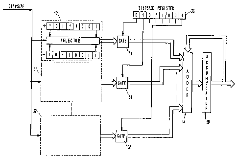
One embodiment of the present invention comprises inclusion of slope error
compensation within the delta-modulation Atop conversion process and more
specifically within the digital re-integration process. Figure 3 illustrates
one method
of compensating slope errors according to the present invention. A number of
selector gates 23,31,...32 are connected to select between a first value
(considered a
positive value;) and a second value (considered a negative value) according to
whether
the sign of thc: up/down step determined by the delta-modulator's comparator
is +
(up) or - (dov~rn). Each pair of positive and negative values is stored in a
corresponding; pair of registers or memory positions. A person skilled in the
art will
appreciate that the arrangement of registers and selectors 30,31,.... 32 can
be
conveniently iimplemented in an integrated circuit by means of a small Random
Access
memory or Electrornically Erasable and Programmable Read Only Memory
(E2PROM) with appropriate addressing arrangements.
CA 02213855 1997-08-26
WO 96/28885 PCT/LTS96/02983
-11-
Each register pair and associated selector corresponds to a particular bit in
the
stepsize register. In the prior art, a bit in the stepsize register indicated
a current
magnitude according to its significance, the bits being always in the series
1, 1/2, 1/4,
1/8.... relative to each other. The sign of the current was indicated by the
stepsign
bit, so the magnitude indicated by a particular stepsize bit was the same
regardless of
sign. The actual positive and negative current sources cannot be perfectly
matched,
thus giving rise. to the slope error. In the arrangement illustrated in Figure
3, the
magnitudes stored in the register pairs are independent for the positive and
negative
stepsign. Moreover, the values associated with different stepsize register
bits are not
constrained to bear a power of two relationship to each other. Rather, each
register
may be prograrnmed with a value representing the actual current of the
positive or
negative current source that is enabled by a particular bit of the stepsize
register.
Thus, when a current source or combination of current sources is enabled to
increase
or decrease the charge on the principal integrator capacitor, the accumulator
38 will
be increased or decreased with an exact corresponding value. This occurs
through
each bit that is equal to a binary "1" in a stepsize register 36 enabling an
associated
gate 33,34,...3:> to pass a selected one of the register values from selector
30,31,...32
through to an adder 37. Thus, the digital values selected to be added in the
adder 37
to the accumulaitor 38 correspond to the analog current source values that are
enabled
by stepsize register 36 and the stepsign bit to sum into the principal
integrator
capacitor. Thus, the accumulator value will follow more accurately the voltage
chaulges on the principal integrator capacitor that in turn follow the wanted
signal
component. The accuracy is optimized by programming values into
register/selector
circuits 30,31,...32 that accurately represent the relative current values of
the positive
and negative current sources. This could, for example, be carried out at the
production stage by means of a calibration procedure in which each current
source
was enabled in turn, its current value measured, and a corresponding digital
value
stored in memory. A non-volatile memory such as E2PROM is normally provided
attached to the .device's main control microprocessor for storing such factory
calibration values. The stored values can later be recalled (on power-up, for
example)
and downloaded into registers 30,31,...32.
CA 02213855 1997-08-26
Wo 96!28885 PC'TIUS96/02983
a
-12-
It is also possible to learn the correct contents of registers 30,31,...32
during
operation. Aftf;r decading a signal segment and determining its information
content,
the deviation of the rExeived signal waveform from the waveform that would be
expected for that information content can be determined inside the digital
signal
processor. The: deviation is expressed as a mean slope or drift over the
signal
segment of the I and ~ waveforms respectively. It is helpful if in addition
the
number of times each current source was enabled to generate a positive current
and
the number of times it generated a negative current are determined by logic
unit 25
incorporating tlae inventive arrangement of Figure 3. Denoting the number of
times
each current source Ii is activated by Ni, then the following equation should
hold:
N1.I1 + N2.I2 ...... + Nm.Im = difference in signal voltage between beginning
and end of
burst.
This may not be solvable to separate the values of Ii after processing only
one signal
segment, but after processing approximately m signal segments there are enough
equations to solve. In practice, the Kalman sequential least squares process
is the
preferred approach for updating the calibration of the Ii values. The Kalman
procedure is a method for solving in the least squares sense all equations
collected to
date, but in an efficient manner that expresses the changes from the previous
best
solution in terms of the most recently acquired equation coefficients. Thus,
the
calibration of trte Ii values can be updated by the Kalman process after
processing
each signal segment.
It may n.ot be necessary to execute the Kalman procedure so often, as the
calibration of hardware-related parameters is not expected to change rapidly.
It is
possible to accumulate a number of the above equations into groups having
similar Ni
values and then to process the accumulated groups only occasionally, in order
to
conserve proce:csor power. For example, if all the equations having N1 as the
largest
coefficient are :summed into a group 1, the sum of the N1 coefficients will
increasingly come to dominate over the sums of the others. Likewise, if all
the
equations having N2 as the largest coefficient are summed into a group 2, then
the
CA 02213855 2004-11-12
-13-
sum of the N2 coefficients will come to dominate. The accumulation of
equations
into m groups in this way will give a cumulative equation set that tends more
to have
a diagonal coefficient matrix, such being the most well-conditioned for
solution either
directly or by the sequential Kalman technique.
An alternative technique for slope compensation is illustrated in Figure 4.
Figure 4 illustrates a pair of I and Q waveforms that are represented by a
sequence of
complex number samples after the digitization process. Initially, it is
assumed the I
and Q accumulators were set to zero just before information bearing signal
samples
were received. Since it could not be known if the received signal plus noise
was
indeed zero at the reset instant, the error known as the arbitrary constant of
re-
integration is introducxd, which however is now of magnitude no greater than
the
wanted signal changes. Figure 4 illustrates I,Q waveforms having both this
constant
offset and a systematic slope. The offsets and slopes are independent for the
I and Q
waveforms and have to be separately determined. One simple method is to simply
fit
the best straight line to the digitized value sequence of the form Y=aX+b.
Curve
fitting techniques are well known in the art. The result of fitting a straight
line in the
least squares sense to the I or Q sequence is to yield a value a, for the
slope of the I
waveform, b, for the constant offset of the I waveform and corresponding
values for
the Q waveform. Then, the slope and offsets are subtracted from the I and Q
waveforms prior to further processing. This simple procedure can suffice in
the case
where signal segments are relatively long such that information modulation
averages
to zero over the segment and does not cause significant inaccuracy in the
determination of the slope and offset. In the case where this is not so, the
initial
estimates of offset and slope can be refined during the decoding of digital
information
which may represent a digitized voice signal as the information waveform
becomes
known and can be subtracted from the determination of slope and offset. For
decoding digital information by means of a Viterbi equalizer, the refining can
be
performed successively after processing each I,Q sample preferably by the
technique
known as "Kalman per Viterbi state" as described in U.S. Patent No. 5,136,616
for
updating frequency error estimates, in U.S. Patent No. 5,204,878 for channel
estimates, and in United States Patent 5,568,518 entitled "Fast Automatic
CA 02213855 2004-11-12
-14-
Gain Control" in regard to channel gain estimates.
In "per-state Kalman", a Viterbi sequential maximum likelihood sequence
estimation procedure for decoding data sequences maintains a number of as-yet
unresolved data sequence hypotheses. Associated with each hypothesis of the
data
sequence to date, an estimate of the slope and offsets of the I,Q waveforms
can be
made with the effect of the hypothesized data sequence removed. For each
state, a
path metric is computed according to known Viterbi techniques and indicates
the
likelihood of the associated data sequence hypothesis being correct. The
collection of
parameters associated with each data sequence hypothesis is known as a "State
Memory". The offset and slope stared in a particular state is used to predict
the next
I,Q value first on the assumption that the next data bit is a 0 and then on
the
assumption that it is a binary 1. The mismatch between the predicted- and
actual I,Q
values is computed and added to the cumulative path metric to obtain new path
metrics. In this way, the number of states is first doubled, but then may be
halved by
selecting to retain only the best of the pairs of states agreeing in all but
their oldest
bits. The retained states comprise data sequence hypotheses that have been
extended
by one data symbol, and the estimates of the slope and offset in each state
may now
be updated on the assumption that the new symbol that has just been added to
each
extended data sequence is true. Finally, the state having the lowest path
metric is
selected to give the decoded data sequence that is most likely to be true, and
the
associated I,Q slopes and offsets are the best estimates of same with that
data
sequence having been specifically accounted for. The slope errors may be used
then,
for example, to correct the Atop conversion process by the means shown in
Figure 3,
or by simpler means such as adjusting the relative values of positive and
negative
current sources by feeding back a control signal. It will be understood by
those
skilled in the art that the digital information can be modulated onto the
radio input
signal using a variety of techniques. For example, the digital information can
be
modulated using manchester-code frequency modulation, Gaussian Minimum Shift
Keying, DQPSK and Pi/4-DQPSK.
CA 02213855 1997-08-26
WO 96/28885 - PCTlHJS96l~?,983
-15-
The im~provernent to zero-IF receivers described above and comprising
correction of h~oth offset and slope compensation of I,Q waveforms is not
meant to be
limiting but ralther exemplary, and a person skilled in the art will be able
to suggest
other means of implementing slope compensation that nevertheless are
considered to
fall within the spirit of the invention as set out in the following claims.
The scope of
the invention is indicated by the appended claims rather than the foregoing
description, and all changes which come within the meaning and range of
equivalents
thereof are intended to be embraced therein.