Language selection

Search

Patent 2213920 Summary

Third-party information liability

Some of the information on this Web page has been provided by external sources. The Government of Canada is not responsible for the accuracy, reliability or currency of the information supplied by external sources. Users wishing to rely upon this information should consult directly with the source of the information. Content provided by external sources is not subject to official languages, privacy and accessibility requirements.

Claims and Abstract availability

Any discrepancies in the text and image of the Claims and Abstract are due to differing posting times. Text of the Claims and Abstract are posted:

  • At the time the application is open to public inspection;
  • At the time of issue of the patent (grant).
(12) Patent Application: (11) CA 2213920
(54) English Title: COMPACT SOLID STATE KLYSTRON POWER SUPPLY
(54) French Title: ALIMENTATTION COMPACTE A SEMI-CONDUCTEUR DE KLYSTRON
Status: Deemed Abandoned and Beyond the Period of Reinstatement - Pending Response to Notice of Disregarded Communication
Bibliographic Data
(51) International Patent Classification (IPC):
  • H03K 03/02 (2006.01)
  • A61N 05/10 (2006.01)
  • H03K 03/57 (2006.01)
  • H03K 17/10 (2006.01)
  • H03K 17/567 (2006.01)
  • H03K 17/60 (2006.01)
(72) Inventors :
  • HITCHCOCK, ROGER N. (United States of America)
  • MARZIALE, MICHAEL J. (United States of America)
  • THOMPSON, LANCE W. (United States of America)
(73) Owners :
  • SIEMENS MEDICAL SYSTEMS, INC.
(71) Applicants :
  • SIEMENS MEDICAL SYSTEMS, INC. (United States of America)
(74) Agent: SMART & BIGGAR LP
(74) Associate agent:
(45) Issued:
(22) Filed Date: 1997-08-26
(41) Open to Public Inspection: 1998-02-28
Examination requested: 2002-08-23
Availability of licence: N/A
Dedicated to the Public: N/A
(25) Language of filing: English

Patent Cooperation Treaty (PCT): No

(30) Application Priority Data:
Application No. Country/Territory Date
08/704,054 (United States of America) 1996-08-28

Abstracts

English Abstract


A high voltage pulse generating circuit for powering klystrons, and the
like. The circuit includes a source of D.C. power having positive and negative
terminals, a flyback transformer having a primary winding and a secondary
winding, the primary winding having first and second terminals for connection
to the source of D.C. power, a sensor for generating a signal indicating the
amplitude of the current in the primary winding, and a solid state switching
circuit for coupling the source of D.C. power to the primary winding of the
flyback transformer. The primary winding is coupled to the power source in
response to a control signal, and decoupled from the power source when a
predetermined level of current is detected in the primary winding.


French Abstract

Cette invention concerne un circuit générateur d'impulsions haute tension pour l'alimentation de klystrons et dispositifs analogues. Le circuit comprend une source de courant continu comportant des bornes négative et positive; un convertisseur indirect ayant un enroulement primaire et un enroulement secondaire, l'enroulement primaire comportant une première et une seconde bornes raccordées à la source de courant continu; un capteur servant à générer un signal d'intensité du courant dans l'enroulement primaire; et un circuit de commutation à semi-conducteur assurant le couplage de la source de courant continu à l'enroulement primaire du convertisseur indirect. L'enroulement primaire est couplé à la source de courant continu en réponse à un signal de commande et découplé de cette même source lorsqu'une intensité prédéterminée de courant est détectée dans l'enroulement primaire.

Claims

Note: Claims are shown in the official language in which they were submitted.


WHAT IS CLAIMED IS:
1. A high voltage pulse generating circuit, comprising:
a source of D.C. power having positive and negative terminals;
a flyback transformer having a primary winding and a secondary
winding, said primary winding having first and second terminals for
connection to said source of D.C. power;
means for generating a signal indicative of current flowing in said
primary winding, said signal indicating the amplitude of said current; and
a solid state switching circuit for coupling said source of D.C. power to
said primary winding of said flyback transformer in response to a control
signal and for decoupling said D.C. power source from said primary winding in
response to said signal indicating that a predetermined level of current was
flowing in said primary winding.
2. The high voltage pulse generating circuit of Claim 1, wherein said
solid state switching circuit comprises first and second IGBTs, said first IGBT
coupling said first terminal of said primary winding to said positive terminal of
said source of D.C. power when said first IGBT is in a conducting state, and
said second IGBT coupling said second terminal of said primary winding to
said negative terminal of said source of D.C. power when said second IGBT
is in a conducting state.
3. The high voltage pulse generating circuit of Claim 1, wherein said
solid state switching circuit further comprises first and second diodes couplingsaid first and second terminals of said primary winding to said positive and
negative terminals of said source of D.C. power.
4. The high voltage pulse generating circuit of Claim 1, further
comprising:
a pulse forming network coupled to said first and second terminals of

said secondary winding; and
a high voltage switch for shorting said pulse forming network in
response to a shorting signal.
5. The high voltage pulse generating circuit of Claim 4, wherein said
high voltage switch includes a plurality of SCR stages, each said SCR stage
comprising an SCR, a resistor, and a control signal generator, said SCR
having an anode, a cathode, and a gate, said SCR conducting current from
said anode to said cathode in the presence of a control signal generating a
potential between said gate and said cathode, said control signal being
generated by said control signal generator, said resistor being connected
between said anode and cathode, said stages being connected such that said
SCR's are connected in series.
6. The high voltage pulse generating circuit of Claim 5, wherein said
control signal generator in each said stage comprises a secondary winding of
a pulse transformer, each said secondary winding being coupled to a
common primary winding.
7. The high voltage pulse generating circuit of Claim 1, wherein said
source of D.C. power is greater than 250 volts and less than 10 kV.
8. The high voltage pulse generating circuit of Claim 1, wherein said
means for generating a signal indicative of current flowing in said primary
winding is a sensor.
9. The high voltage pulse generating circuit of Claim 1, further
comprising a pulse forming network coupled to said first and second terminals
of said secondary winding, said pulse forming network including inductors
with slugs, said slugs capable of varying an inductance of said pulse forming

network.
10. A high voltage pulse generating circuit in a radiation treatment
device, comprising:
a radiation source capable of generating a radiation beam having a
variable radiation output;
a source of D.C. power having positive and negative terminals;
a flyback transformer having a primary winding and a secondary
winding, said primary winding having first and second terminals for
connection to said source of D.C. power; and
means for generating a signal indicative of current flowing in said
primary winding, said signal indicating the amplitude of said current;
wherein said D.C. power, said flyback transformer and said means for
generating a signal are used to supply power to said radiation source such
that said radiation beam is generated.
11. The high voltage pulse generating circuit in a radiation treatment
device of claim 10, further comprising a solid state switching circuit for
coupling said source of D.C. power to said primary winding of said flyback
transformer in response to a control signal and for decoupling said D.C.
power source from said primary winding in response to said signal indicating
that a predetermined level of current was flowing in said primary winding.
12. The high voltage pulse generating circuit in a radiation treatment
device of Claim 11, wherein said solid state switching circuit comprises first
and second IGBTs, said first IGBT coupling said first terminal of said primary
winding to said positive terminal of said source of D.C. power when said first
IGBT is in a conducting state, and said second IGBT coupling said second
terminal of said primary winding to said negative terminal of said source of
D.C. power when said second IGBT is in a conducting state.

11
13. The high voltage pulse generating circuit in a radiation treatment
device of Claim 11, wherein said solid state switching circuit further comprisesfirst and second diodes coupling said first and second terminals of said
primary winding to said positive and negative terminals of said source of D.C.
power.
14. The high voltage pulse generating circuit in a radiation treatment
device of Claim 10, further comprising:
a pulse forming network coupled to said first and second terminals of
said secondary winding; and
a high voltage switch for shorting said pulse forming network in
response to a shorting signal.
15. The high voltage pulse generating circuit in a radiation treatment
device of Claim 14, said high voltage switch including a plurality of SCR
stages, each said SCR stage comprising an SCR, a resistor, and a control
signal generator, said SCR having an anode, a cathode, and a gate, said
SCR conducting current from said anode to said cathode in the presence of a
control signal generating a potential between said gate and said cathode,
said control signal being generated by said control signal generator, said
resistor being connected between said anode and cathode, said stages being
connected such that said SCR's are connected in series.
16. The high voltage pulse generating circuit in a radiation treatment
device of Claim 15, wherein said control signal generator in each said stage
comprises a secondary winding of a pulse transformer, each said secondary
winding being coupled to a common primary winding.
17. The high voltage pulse generating circuit in a radiation treatment
device of Claim 10, wherein said first and second terminals of said secondary
winding are a pulse forming network, said pulse forming network including

12
inductors with slugs, said slugs capable of varying an inductance of said
pulse forming network.

Description

Note: Descriptions are shown in the official language in which they were submitted.


~ 96 P 7532 CA 02213920 1997-08-26
COMPACT SOLID STATE KLYSTRON PC~WER SUPPLY
Field of the Invention
The present invention relates to power supplies, and more particularly,
to a compact power supply for use in powering linear accelerators, and the
5 like.
Background of the Invention
Radiation-emitting devices are generally known and used, for instance
as radiation therapy devices for the treatment of patients. A radiation therapy
device generally comprises a gantry which can be swiveled around a
l 0 horizontal axis of rotation in the course of a therapeutic treatment. A linear
accelerator is located in the gantry for generating a high energy radiation
beam for therapy. This high energy radiation beam can be an electron or
photon (X-ray) beam. During treatment, this radiation beam is trained on one
zone of a patient Iying in the isocenter of the gantry rotation.
I5 In this arrangement, radiation is generated by applying an electron
beam to a target to generate x-rays. The electron beam is typically generated
in a linear accelerator that is powered by a klystron based power supply
having a power output in the 10 to 30 kW range. Figure 1 is a block diagram
of a medical linear accelerator showing major components and auxiliary
20 systems. Power supply 10 provides D.C. power to modulator 12. Modulator
12 includes a pulse forming network and a switch tube known as hydrogen
thyratron. A thyratron is a low pressure gas device with a thermionic cathode.
Over time, the cathode depletes itself. Thus, a thyratron has an inherent
wear out mechanism. The high voltage pulses from modulator 12 are flat-
25 topped D.C. pulses of a few microseconds in duration. These pulses aredelivered to magnetron or klystron 14 and simultaneously to electron gun 16.
Pulsed microwaves produced in magnetron or klystron 14 are injected into
accelerator tube 20 via waveguide system 22. At the proper instant,

CA 02213920 1997-08-26
electrons, which are produced by electron gun 16, are also pulse injected into
accelerator tube 20. High energy electrons emerge from accelerator tube 20
in the form of a beam of approximately 3 mm in diameter. These electrons
can be fed to treatment head 24 as a straight beam or to treatment head 26
s as a bent beam. If the electrons are sent to treatment head 26, the electrons
are bent by, for example, bending magnet 28 through a suitable angle (e.g.,
270 degrees) between accelerator tube 20 and the target.
Prior art power supplies for linear accelerators are large, heavy devices
that significantly increase the cost and size of the medical treatment system.
I0 One typical prior art system utilizes a high voltage transformer/rectifier system
to generate a 21 kV DC power source from a conventional three-phase 208 V
power source. The high voltage DC source is then used to generate a 15 kV
pulse that is converted to the required 150 kV pulse via a high voltage pulse
transformer. The high voltage transformer/rectifier assembly typically weighs
l 5 500 Ibs. and occupies 8 cubic feet. As a result, the power supply must be
housed in a separate cabinet from the linear accelerator. In addition to
increasing the floor space needed to house the accelerator system, this
additional cabinet requires special power transmission lines to couple the
klystron output to the linear accelerator which further increases the cost and
20 complexity of the system. Finally, the sheer weight of the system increases
the cost of shipping.
Broadly, it is the object of the present invention to provide an improved
high voltage power system for powering klystrons and the like. It is a further
object of the present invention to provide a high voltage power system that
25 requires less space than prior art high voltage power systems. It is a still
further object of the present invention to provide a high voltage power system
that is significantly lighter than prior art power supply systems. These and
other objects of the present invention will become apparent to those skilled in
the art from the following detailed description of the invention and the
30 accompanying drawings.

. CA 02213920 1997-08-26
Summary of the Invention
The present invention is a high voltage pulse generating circuit for
powering klystrons and the like. In one embodiment, the invention is used in
a radiation treatment device. The high voltage pulse generating circuit
S includes a source of D.C. power, a flyback transformer, a sensor and a solid
state switching circuit. The source of D.C. power has positive and negative
terminals. The flyback transformer has a primary winding and a secondary
winding. The primary winding in the flyback transformer has first and second
terminals for connection to the source of D.C. power. The sensor generates a
10 signal indicating the amplitude of the current in the primary winding. The solid
state switching circuit couples the source of D.C. power to the primary
winding of the flyback transformer. The primary winding is coupled to the
power source in response to a control signal, and decoupled from the power
source when a predetermined level of current is detected in the primary
1 5 winding.
Brief Description of the Drawin~s
Figure 1 is a block diagram of a medical linear accelerator showing
major components and auxiliary systems;
Figure 2 is a block diagram of a typical prior art power supply system
20 for operating a klystron for driving a linear accelerator;
Figure 3 is a block diagram of one embodiment of a high voltage power
system according to the present invention;
Figure 4 is a schematic diagram of a power switch according to the
present invention;
Figure 5 is a schematic diagram of a high voltage switch according to
the present invention; and
Figure 6 is a block diagram of the pulse forming network in the
preferred embodiment.

. CA 02213920 1997-08-26
Detailed Description of the Invention
The manner in which the present invention gains its advantages over
the prior art may be more easily understood with reference to Figure 2 which
is a block diagram of a typical power system 50 for powering a klystron.
5 Power system 50 converts 208 volt, 3 phase power to 15 kV, 1200 amp.
pulses of approximately 5 ,us duration. These pulses are stepped up to 150
kV by pulse transformer 85 whose output drives the klystron. The 15 kV
pulses are generated by a pulse generating circuit that is powered by a 21 kV
D.C. source. The 21 kV D.C. source is typically a high voltage transformer
I 0 and rectifier assembly 60. As noted above this D.C. power supply typically
occupies 8 cubic feet and weighs approximately 500 Ibs.
The high voltage pulse generating circuit typically consists of an
inductor 72 which resonantly charges a pulse forming network 76. The final
pulse amplitude that is applied to the klystron is adjusted by controlling the
IS amount of time a high voltage charge switch 71 is closed. The system
measures the current flowing through a resistor 73 and the voltage at the
pulse forming network 76 to determine the timing of the switch opening. The
connection to the pulse forming network has been omitted from the drawing.
A controller 74 utilizes the current and voltage measurements to control the
20 switch closure duration. It should be noted that the range of adjustment in the
final pulse amplitude that can be obtained with the inductor design shown in
Figure 2 is limited because only a portion of the energy of the final pulse is
stored in inductor 72. It should also be noted that the conversion of the 208
volt power to a 21 kV D.C. source requires a substantial number of high
25 voltage components that must operate at high power levels which require
high voltage insulation and pose safety problems.
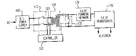
Figure 3 is a block diagram of a high voltage power system 100
according to the present invention. The present invention utilizes a flyback
transformer 120 to power pulse forming network 176. Flyback transformer
30 120 is powered from a 300 volt D.C. power supply 102. This is a significant
reduction from the 21 kV D.C. power supply used in the prior art. A solid

CA 02213920 1997-08-26
.
state switch 110 is used to control the output voltage from flyback transformer
120. A controller 122 senses the current flowing in the primary of flyback
transformer 120, as shown at 121. When the current reaches the desired
level, switch 110 is opened, and the energy stored in flyback transformer 120
5 is transferred to pulse forming network 176. After pulse forming network 176
is charged, high voltage switch 175 is closed to discharge pulse forming
network 176 thereby transferring the energy stored in pulse forming network
176 to the primary of pulse transformer 185. The operation of pulse forming
network 176 and pulse transformer 185 are substantially the same as
10 described above with respect to the typical klystron power system shown in
Figure 2.
It should be noted that flyback transformer 120 stores 100 percent of
the energy that is later transferred to the klystron pulse. Hence, the present
invention provides a greater range of control over the output pulse amplitude
15 sent to the klystron. The control of the pulse amplitude is also simplified by
the present invention. The pulse amplitude is controlled by opening switch
110 in response to a predetermined current being sensed in the primary of
flyback transformer 120. Switch 110 operates at only 300 volts, in contrast to
switch 71 shown in Figure 2 which must operate at 21 kV. Hence, a
20 significant savings in cost is achieved in addition to improved reliability and
safety.
Further, since flyback transformer 120 is driven by a low voltage power
source, the problems associated with the high voltage power supply are
avoided. Power supply 102 requires approximately 1/4 cubic feet of space
25 and weighs only about 5 Ibs (an 800 Ib weight reduction). In addition, the
lower operating voltage provides increased safety and reliability.
The basic flyback transformer design shown in Figure 3 has been used
in low power systems for some time. However, practical realizations of such
a power supply for high power output have not been heretofore available. In
30 particular, a practical implementation of switch 110 has been lacking. The
vacuum tetrode used in the prior art contains an inherent wear out

CA 02213920 1997-08-26
mechanism (the catl1ode), thus a solid state design is more desirable. In the
present invention, switch 110 is implemented as a pair of insulated gate
bipolar transistors (IGBTs).
Figure 4 is a schematic drawing of a power switch 200 according to the
5 present invention. Power switch 200 utilizes two switching circuits shown at
210 and 220. Each switching circuit includes an IGBT 211 and a shunt diode
212. Switching circuits 210 and 220 are commercially available. Switching
circuits 210 and 22Q connect the D.C. power supply to the primary of flyback
transformer 120. When switching circuits 210 and 220 disconnect the primary
l O of flyback transforn~er 120 a reverse potential is generated across the primary
winding. Shorting diodes 231 and 232 prevent this potential from damaging
switching circuits 210 and 220, respectively. Shorting diodes 231 and 232
redirect this energy to the D.C. power supply where it is stored in the filter
capacitors therein. As a result, the power is recovered for use in the next
15 pulse.
In the preferred embodiment of the present invention, high voltage
switch 175 (see Figure 3) is implemented as a high voltage semiconductor
controlled rectifier (SCR) stack (i.e., a number of SCRs in series). In prior art
systems, the analogous switch is typically implemented with a gas thyratron
20 which is less reliable and more costly than the SCR stack used in the presentinvention. The preferred embodiment of a high voltage switch according to
the present invention is shown in Figure 5 at 300. Switch 300 is constructed
from a number of SCR stages connected in series. The first, second, and last
stages are shown at 310, 320 and 340, respectively. Each stage includes an
25 SCR in parallel with a resistor and a capacitor, the resistor and capacitor
being connected between the anode and cathode of the SCR. For example,
stage 310 includes SCR 311, capacitor 312 and resistor 313. The capacitors
and resistors are also connected in series to form a voltage divider network.
The voltage divider assures that the same voltage is applied across each of
30 the SCRs when the SCRs are not conducting. In the absence of the voltage
divider, differences in the impedances of the SCRs in the non-conducting

CA 02213920 1997-08-26
state can lead to different potentials being realized across each SCR when
the SCR stack is not conducting. This can result in one of the SCRs being
subjected to a potential difference in excess of its breakdown voltage.
The stack is triggered by coupling a signal through the inductor 316 in
5 each stage. These inductors are the secondary stage of a pulse transformer
350, the signal being applied to the primary 351 of pulse transformer 350.
Each stage includes a resistor and zener diode that assures that the trigger
voltage between the gate and cathode of the SCR in each stage are the
same for each stage. The resistor and zener diode in the first stage are
lO shown at 314 and 315, respectively.
In the pulse forming network, the inductor design is improved. In
particular, the inductance is made to be adjustable while the system is
running. Figure 6 is a block diagram of the pulse forming network in the
preferred embodiment. Pulse forming network 400 includes inductors 410-
15 416. Usually, in a pulse forming network, a clip is placed on the inductors andthe system must be shut down to manually change the inductance. The
inductance is changed to fine tune the wave shape provided by the pulse
forming network. This shutting down of the system and reviewing the wave
shape is typically done repeatedly until the desired wave shape is obtained.
20 A specially trained individual requires approximately 1 hour to fine tune the wave shape. In contrast, the present design uses aluminum slugs 420-426
which are placed inside inductors 410-416. Each of aluminum slugs 420-426
can be moved up and down while the system is running to vary the
inductance and fine tune the wave shape. Aluminum slugs 420-426 can be
25 moved either manually or automatically. With this improved design, fine
tuning takes approximately 3 minutes.

Representative Drawing
A single figure which represents the drawing illustrating the invention.
Administrative Status

2024-08-01:As part of the Next Generation Patents (NGP) transition, the Canadian Patents Database (CPD) now contains a more detailed Event History, which replicates the Event Log of our new back-office solution.

Please note that "Inactive:" events refers to events no longer in use in our new back-office solution.

For a clearer understanding of the status of the application/patent presented on this page, the site Disclaimer , as well as the definitions for Patent , Event History , Maintenance Fee  and Payment History  should be consulted.

Event History

Description Date
Inactive: IPC from MCD 2006-03-12
Application Not Reinstated by Deadline 2005-04-15
Inactive: Dead - No reply to s.30(2) Rules requisition 2005-04-15
Deemed Abandoned - Failure to Respond to Maintenance Fee Notice 2004-08-26
Inactive: Abandoned - No reply to s.30(2) Rules requisition 2004-04-15
Inactive: S.30(2) Rules - Examiner requisition 2003-10-15
Letter Sent 2002-09-30
Request for Examination Requirements Determined Compliant 2002-08-23
Request for Examination Received 2002-08-23
All Requirements for Examination Determined Compliant 2002-08-23
Application Published (Open to Public Inspection) 1998-02-28
Inactive: IPC assigned 1997-11-17
Inactive: IPC assigned 1997-11-14
Classification Modified 1997-11-14
Inactive: First IPC assigned 1997-11-14
Inactive: Filing certificate - No RFE (English) 1997-10-29
Letter Sent 1997-10-29
Application Received - Regular National 1997-10-29

Abandonment History

Abandonment Date Reason Reinstatement Date
2004-08-26

Maintenance Fee

The last payment was received on 2003-07-21

Note : If the full payment has not been received on or before the date indicated, a further fee may be required which may be one of the following

  • the reinstatement fee;
  • the late payment fee; or
  • additional fee to reverse deemed expiry.

Patent fees are adjusted on the 1st of January every year. The amounts above are the current amounts if received by December 31 of the current year.
Please refer to the CIPO Patent Fees web page to see all current fee amounts.

Fee History

Fee Type Anniversary Year Due Date Paid Date
Application fee - standard 1997-08-26
Registration of a document 1997-08-26
MF (application, 2nd anniv.) - standard 02 1999-08-26 1999-07-23
MF (application, 3rd anniv.) - standard 03 2000-08-28 2000-07-18
MF (application, 4th anniv.) - standard 04 2001-08-27 2001-07-12
MF (application, 5th anniv.) - standard 05 2002-08-26 2002-07-22
Request for examination - standard 2002-08-23
MF (application, 6th anniv.) - standard 06 2003-08-26 2003-07-21
Owners on Record

Note: Records showing the ownership history in alphabetical order.

Current Owners on Record
SIEMENS MEDICAL SYSTEMS, INC.
Past Owners on Record
LANCE W. THOMPSON
MICHAEL J. MARZIALE
ROGER N. HITCHCOCK
Past Owners that do not appear in the "Owners on Record" listing will appear in other documentation within the application.
Documents

To view selected files, please enter reCAPTCHA code :


To view images, click a link in the Document Description column. To download the documents, select one or more checkboxes in the first column and then click the "Download Selected in PDF format (Zip Archive)" or the "Download Selected as Single PDF" button.

List of published and non-published patent-specific documents on the CPD .

If you have any difficulty accessing content, you can call the Client Service Centre at 1-866-997-1936 or send them an e-mail at CIPO Client Service Centre.


Document
Description 
Date
(yyyy-mm-dd) 
Number of pages   Size of Image (KB) 
Representative drawing 1998-03-12 1 7
Abstract 1997-08-25 1 21
Description 1997-08-25 7 342
Claims 1997-08-25 5 176
Drawings 1997-08-25 3 69
Courtesy - Certificate of registration (related document(s)) 1997-10-28 1 116
Filing Certificate (English) 1997-10-28 1 164
Reminder of maintenance fee due 1999-04-26 1 111
Reminder - Request for Examination 2002-04-28 1 118
Acknowledgement of Request for Examination 2002-09-29 1 177
Courtesy - Abandonment Letter (R30(2)) 2004-06-24 1 166
Courtesy - Abandonment Letter (Maintenance Fee) 2004-10-20 1 178