Note: Descriptions are shown in the official language in which they were submitted.
~ CA 02214241 1997-08-29
'
PATENT
RMS CONVE~T}3:R USING DIGIT~L FILTl~RING
Back~round of the In~ention
This invention relates generally to root mean square (rrns) converter circuits and
in particular to an rms converter for determining the rms value of a signal with no
knowledge of the signal period.
The ability to det~rmine the rms value of signals having arbitrary waveshapes with
high accuracy and reliability is of great importance in test and measurement equipment.
Most multimeters and voltmeters used for measuring alternating current (a.c.) line voltage
provide a facility to do so in terms of volts rrns as the most meaningful measurement
rather than volts peak-peak. Early multimeters used a diode rectifiers and averaging
circuits to provide measurements in terms of volts rms. Such an arrangement provided
accurate readings only when the signal has a sinusoidal waveshape but will produce
measurément errors often in excess of lO'~o for other types of waveshapes such as square
waves.
RMS to d.c. converters improve on the lirnitations of the diode averaging by
producing a "true-rrns" value in the form of a d.c. voltage for signals having a much
wider variety of waveshapes. Thermal rms converters are a variety of rms convèrters that
operate by applying a signal having an arbitrary waveshape to a resistor in a therrn~lly
isolated environment. The power dissipated in the resistor is proportional to the square of
the voltage of the signal which produces a telnpc,aLure rise. The temperature rise and the
equivalent heating power of the signal in the resistor is duplicated in a second, m~tl hed
resistor by ad3usting a d.c. voltage. The d.c. voltage thus produced corresponds to the rms
value of the signal with no regard to the period or waveshape of the signal.
A therrnal rms converter using thermally isolated, matched resistors is discussed
in U.S. Patent 4,346,291, "Thermally Isolated Monolithic Semiconductor Die", issued
~ ~ CA 02214241 1997-08-29
August 24, 1982, to Chapel, Jr. et al., E:luke Corporation, assignee. A circuit for
increasing the accuracy of thermal rms converters is discussed in U.S. Patent 4,274,143,
"Recirculating RMS AC Conversion Method and Apparatus", issued June 16, 1981, toBrodie, et al., l~luke Corporation, assignee. Thermal rms converters, while allowing for
- s relatively high accuracy rms to d.c. conversions if care~ully implemented, are relatively
expensive and complex to manufacture, are easily destroyed, and have relatively slow
response times.
Another variety of rms to d.c. converter is the monolithic rms converter which
employs analog circuits such as amplifiers, multipliers, dividers, and integrators within a
lo single integrated circuit. Monolithic rrns converters are commercially available, relatively
inexpensive to produce, and can handle a wider variety of waveshapes than the diode
averaging techniques. Several types of monolithic rrns converters exist in the prior art
including explicit rms converters as shown in FIG. 1 and implicit rrns converters as
shown in ~;IG 2.
1~ ~s shown in FIC~. 1, an explicit rms converter 10 accepts the input signal, squares
it in a squaring circuit, averages the squared value over a predetermined averaging period
in an averaging circuit 14 comprising a resistor R, a capacitor C, and a buffer 16,, and
then takes the square root in a square root circuit 18 to obtain a d.c. signal Vout that is
representative of the rms level of the input signal. The capacitor C and resistor R together
20 comprise a one-pole ~llter circuit and have values selected according to the predetermined
averaging period. The capacitor ~ is usually the only external component that must be
added to the explicit rms converter. The value of the averaging capacitor also determines
the low frequency accuracy, ripple level, and settling time of the monolithic rms
converter, all of which must be traded off for each particular application. Because the
2~ squaring circuit may develop voltages that vary enormously in response to the input
signal, the dynamic range of the explicit rms converter 10 is relatively limite~l
. ' - CA 02214241 1997-08-29
?
In E~IG. 2, there is shown an implicit rrns converter 20 in which the input signal is
accepted by a squarer-divider circuit 22 which performs the square root functionimplicitly without having to actually produce the square of the amplitude of the input
signal, thereby increasing the effective dynamic range so that a greater range of input
signal amplitudes may be accommodated. The output of the squarer-divider is provided
to an averaging circuit 24 which is comprised of the one-pole filter using the resistor R
and the capacitor C and a buffer 26 to develop the output signal Vout. Most monolithic
rms converters operate using some form of the implicit rms converter method in order to
get around the dynamic range iimitation of the explicit rrns converter topology.0 In either the explicit or implicit rms converter topologies, in order to obtain rms to
d.c. conversions within a specified degree of accuracy in a monolithic rms converter, the
input signal being measured is subject to several restraints. First, the input signal must be
periodic. Second, the predetermined averaging period set by the value of the averaging
capacitor must be long enough to allow averaging multiple signal periods in order to
reduce the ripple component in the output signal. As noted above, the filtering circuit is
typically a one-pole filter. Finally, the input signal must have less than a certain crest
factor which is de~lned as the peak value of an input signal divided by its rms value.
Thus, the input signal being measured cannot be truly arbitrary and erroneous
measurement results may be obtained if the input signal deviates from any of these
constraints.
Because of gain-bandwidth limitations of their analog circuits, monolithic rms
converters also suffer from bandwidth variations as a function of input signal amplitude.
To obtain the flattest bandwidth, which is the output signal level in response to a constant
input voltage over a frequency range of interest, the input signal should be adjusted so
2s that the ma~imum rms signal level corresponds to the full scale input level of the
monolithic rms converter.
.; ~ CA 02214241 1997-08-29 '.
Analog-to-digital converters (ADCs), which had formerly been placed behind the
monolithic rms converter to convert the d.c. voltage into digital samples, are now
comInonly replacing the monolithic rms converter in newer instrument designs to
measure input signals at the front end. ADCs now provide higher sampling rates and
s measurement accuracy that allow for sampling the signal directly and storing the digital
measurement values as a time record. Using m~th~m~tical operations that integrate the
signal voltage over a predetermined number of digital measurement values from the time
record, the rms value of the signal can be calculated. However, this mathematical method
requires that the input signal be periodic and that the signal period be known. If the signal
10 period is unknown or the signal is aperiodic, a default period must be chosen for the
calculation which may lead to erroneous results.
Therefore, it would be desirable to provide a method and apparatus for measuringrms values from digital samples with no requirement that the period of the signal being
measured be known or evén that the signal be periodic.
Summarv of the Invention
In accordance with the present invention, an rms converter using digital samples is
provided. The rms converter is implemented using a squaring circuit followed by an rms
digital filter and a square root circuit. Each digital sample from the ADC is squared and
20 then presented to a digital filter where it is filtered in a continuous fashion to produce rms
values.
The transfer function of the rms digital filter of the present invention is modeled
after the thermodynarnic principles of applying a signal to a temperature sensitive resistor
in the manner of the thermal rrns converter. In this way, the rrns value may be obtained
25 using a stream of digital samples from a signal without regard to the period of the signal
while avoiding the difficulties of providing thermally isolated matched resistors or in
having to choose an integration period to calculate the rms value.
~ ' CA 02214241 1997-08-29 ''.
According to the thermodynarnic model, the resis~or heats up according to the
power in the signal applied across it such that the power dissipated in the resistor is
proportional to the square of the signal voltage. The resistor heats to an equilibrium point
where the energy added is equal to the energy lost. Ithe rrns value of the signal at this
s- equilibrium point is the same as the amplitude of a d.c. signal that heats the resistor to the
same temperature. As such, the resistor acts as ~llter for the energy applied to it and the
signal period is not relevant to its operation. There is no requirement that the signal be
periodic because this filtering action takes place continuously.
~n modeling the thermodynarnic behavior of the resistor, the rrns digital filter may
0 be implemented in its simplest form as an inflnite Impulse response (DR) filter according
to the following general equation
Yn = axn2 ~ bYn l
in which the f1lter constants a and b are chosen so that
a~b= 1
The rms digital filter is then implemented according to following equation:
Yn = a(xn) - aYn 1 + Yn-l
where:
Yn is the present filtered digital sample
Yn l is the past filtered digital sample
Xn is the present digital sample
In an equilibrium state, Yn = Yn-l and added energy, represented by a(xn)Z, equals
energy lost, represented by aYn l, making Yn and Xn steady values. Therefore, Xn is
equivalent to a steady d.c. value which is the square root of Yn and thus represents the
rrns value.
2s The rrns digital filter within the rms converter of the present invention extends
this fundamental concept by having a transfer function that is essen~i~lly a low pass filter
that extracts the rms value from the stream of digital samples in a continuous manner thus
~ CA 02214241 1997-08-29 --
requiring no knowledge of the period of the signal. The squaring and rms digital ~lltedng
operations take place in real-time using each digital measurement value as it arrives.
Next, a square root of the digital measurement values is taken, preferably only when a
display update is made, to obtain the present rms value from the rms filter. ~ addition,
s the rms digital filter is optimi7ecl in terms of. settling time, stop band frequency and
attenuation, pass band ripple, and other ~llter parameters using optimi7~tion techniques
known in the art. For a given accuracy and resolution, the rms digital filter can be
optimized to provide faster responses than prior art rms converters.
In a measurement instrurnent for measuring rms values employing the rrns
0 converter according to the present invention, an input signal is connected to a front end
circuit which scales the signal amplitude to allo~ for proper sampling by a sampling
system. A measurement bandwidth, which is typically deterrnined as a design
requirement for the measurement instrument, ~eterrnines the minimllm sample rateneeded for the sampling system. Frequency components in the input signal beyond the
15 measurement bandwidth would not be measured. The sampling system may comprise a
sigma-delta converter followed by a decimation filter or alternatively a conventional
ADC. The sampling system samples the input signal having an arbitrary waveshape to
provide the digital samples at a sample rate to the rms converter. The rms values
developed as described above from the rms converter are provided to a display on the
20 measurement instrument, typically at an update rate clett~.rrnined by a microprocessor.
One obJect of the present invention is to provide an rrns to d.c. converter thatoperates independently of the signal period.
Another object of the present invention is to provide an rms converter comprising
a squaring circuit, a digital filter, and a square root circuit that operate on digital samples
2s independently of the signal period.
An additional ob3ect of the present invention is to provide an rms converter
having constant bandwidth over a wide range of input signal amplitudes.
~ - CA 02214241 1997-08-29
A further object of the present invention is to provide a method for providing rms
values using a digital filter to extract the rrns values from a stream of digital samples.
Other features, ~tt~inmentS~ and advantages will become apparent to those skilled
in the art upon a reading of the following description when taken in conjunction with the
s accompanying drawings.
Brief Description of the Drawin~s
FIG. 1 is a drawing of an explicit rms converter according to the prior art;
FIG. 2 is a drawing of an implicit rms converter according to ~e prior art;
FIG. 3 is a dra~ving of a measurement instrument as applied in measuring the rmsvalue of an a.c. signal of unknown period and waveshape;
FI~. 4 is a simplified block diagram of the measurement instrument of FIG. 3
according to the preferred embodiment of the present invention;
FIG. S is a simpli~led block diagram of the measurement instrument of FIG. 3
according to an alternative embodiment of the present invention; and
FIG. 6 is a simplified block diagram of the rms converter according to the present
invention.
Detailed DescriPtion of the Invention
FIG. 3 is a drawing (not to scale) of a measurement instrument 110 coupled via
test leads 112a and 112b to a voltage source 114 to obtain an input signal. The
measurement instrument 110 is designed to be applied in service, installation, and
maintenance environments in which a variety of input signals having a variety ofwaveshapes may be encountered. The measurement instrument 110 may be implementedin the form of a digital mllltimeter, an oscilloscope, or other measurement instrument for
2s me~ ring input signal voltages.
The input signal provided by the voltage source 114 may be an alternating current
(a.c.) signal, a direct current (d.c.) signal or a combination of a.c. plus d.c. on the same
~ ~ CA 02214241 1997-08-29 -
waveform. The input signal may have a sinusoidal waveshape with a stable period or it
may simply be random noise with no period or discernible waveshape. It is desirable that
the measurement instn~ment 110 be capable of displaying the rms (root-mean-square)
value of the input signal without any knowledge of its period or waveshape within a
s - desired measurement bandwidth.
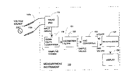
FIG. 4 is a simplified block diagram of the measurement instrunient 110 (sho~n
in FIG. 3) according to the preferred embodiment of the present invention. The voltage
source 14 is coupled via the test leads 112a and 112b to a front end 116 within the
measurement instrument 110. The front end 116 may contain over~voltage and over-
o current protection circuits, amplifiers, attenuators, and filters in order to provide a scaledinput signal of suitable amplitude level and bandwidth for conversion into digital
samples.
Sigma-delta converter 118 is an over-sampling type analog to digital converter
.
(ADC) which generates raw sample data at a sample rate substantially higher than the
5 Nyquist rate for a selected measurement bandwidth, as is known in the art. The raw
sarnple data may be converted to digital samples at base band using a decimation filter
120 as is also known in the art. In the preferred embodiment, the measurement
bandwidth was chosen to be 500 kilohertz, with the sigma-delta converter 118 operating
at a sample rate of ten megasamples per second ( 10 MS/s) for a 20:1 ratio. The sigma-
20 delta converter 118 generates the raw sample data with a resolution of 5 bits which issupplied to the decimation filter 120 which low-pass filters the raw sample data to
provide digital samples at 2.5 MS/s with a resolution of 14 bits.
The decimation filter 120 may be implemer-tç~ as a finite impulse response (FIR?filter, as a infinite impulse response (I~) filter, or as a hybrid of FIR and IIR filters, with
2s the filter constants and structure chosen to obtain a desired transfer function. The sigma-
delta converter topology is desirable because no precision components are needed in the
converter, thus allowing for the circuitry to be implemented easily as a monolithic
, ' -; CA 02214241 1997-08-29 ~
integrated circuit as is known in the art. The sigma-delta converter 118 and clecim~tion
filter 120 collectively compnse a sampling system 121 which converts the input signal to
a stream of digital samples according to a sample rate.
The digital samples are provided as a continuous data stream at a rate of 2.5 MS/s
to an rms converter 122. The rms converter 122 processes each of the digital samples in
the continuous data stream as they arrive with no knowledge of the periodicity or
waveshape of the input signal, as explained in more detail below. A microprocessor 124
receives rms values produced by the rrns ~1lter and selectively provides the rms values to
a display 126 where they mav be displayed in numerical or graphical format as desired.
0 The rms values may be provided continuously or in response to an update signal from the
microprocessor 124.
The rms converter 122 offers a number of advantages over the prior art
particularly when applied in the measurement instrument 110 as a handheld, battery-
operated package. The sigma-delta converter 118, the decimation filter i20 and the rms
converter 122 may all be implemented as monolithic integrated circuits, with a minimnm
of external precision components, thus reducing cost, board space, power consumption,
and m~llf~ctllring complexity.
The rms converter 122 ~urther offers substantial perforrnance advantages over the
prior art. The crest factor, a substantial limitation in monolithic rms converters, is limited
in the present invention only by the sampling system 21 and word length of the rrns
digital filter 132. At the same time, the a.c. bandwidth of the rms converter 122 is
constant, being de~med according the ~llter constants applied in the rms digital filter 132.
Furthermore, the performance of the rms converter 122, defined in terms of transfer
function and a.c. bandwidth, are substantially constant over a wide range of amplitudes of
2s the input signal. The rms digital filter 132 may have as many poles as needed to achieve
adequate stopband rejection of a.c. ripple components while m~int~inin~ a desired
settling time and no overshoot in its pulse response characteristic.
' ' CA 02214241 1997-08-29
FIG. S is a simplifled block diagram of the measurement instrument 110 (shown
in FIG. 3) according to an alternative embodiment of the present invention in which the
sampling system 121 consists of an analog-to-digital converter (ADC) 128. The voltage
source 114 is coupled via the test leads 112a and 112b to a front end 116 within the
s measurement instrument 110. The front end 116 may contain over-voltage and over-
current protection circuits, ampli~lers, attenuators, and filters in order to provide the input
signal of suitable amplitude level and bandwidth to the sampling system 121.
The ADC 118 generates digital samples at a sample rate higher than the Nyquist
rate which is twice the measurement bandwidth, as is known in the art. Because the
measurement bandwidth was chosen to be 500 kilohertz, the ADC 128 must operate at a
sample rate exceeding 1 MS/s and preferrably at 10 MS/s, with the actual sample rate
driven by considerations of conversion accuracy. Other ADC technologies may be
readily substituted for the ADC 118, with consideration given to component cost,maximum sample rate, power consumption, as well as converter accuracy and resolution,
.
1~ to provide digital samples representative of the input signal to the rms converter 122.
The digital samples are provided as a continuous data stream from the ADC~ 128
to the rms converter 122. The rms converter 122 processes each of the digital samples in
the continuous data stream as they arrive with no knowledge of the periodicity or
waveshape of the input signal, as explained in more detail below. A microprocessor 124
20 réceives the rms values produced by the rms converter and selectively provides the rms
values to a display 126 where they may be displayed in numerical or graphical format as
desired. The rms values may be provided continuously or in response to an update signal
from the microprocessor 124.
FIG. 6 is a simplified block diagram of the rms converter 122 according to the
2s present invention. Digital samples from the sigma-delta converter 118 and decimation
filter 120 as shown in FIG. 4 or the ADC 128 as shown in FIG. S arrive at the rms
converter 122. Each digital sample is squared in the squaring circuit 130 to produce
- 10-
. . - CA 02214241 1997-08-29 -
squared digital samples. Each squared digital sarnple is provided to an rms digital filter
132 which has filter coefficients chosen to allow the rms digital filter 132 to operate as a
low pass filter. The filter coef~lcients and digital filter topology may be designed
according to known IIR and ~;IR techniques, or a combination of FIR and IIR techniques,
s to provide a low pass filter having desired characteristics. In the preferred embodiment,
the rms digital filter 32 has the following characteristics:
measurement bandwidth 500 kilohertz maximum
stopband of -123 decibels 49.9 hert~ maximum
settling time to 0.001% of ~mal value 0.5 seconds maximum
0 step response overshoot 0.0% maximum
output data rates 0.12~, 0.5, 2, and 1000 hertz
In the digital rms filter 132, it was important that there be no overshoot in the step
response along with a high stopband rejection of 50/60 hertz ripple from power line
... .. . .. .
- frequencies. Filtered rms values produced by the digital rms filter 132 are provided to a
15 square root circuit 134 which produces the rms value by taking the square root of the
present filtered rms value, either continuously or as needed in response to the update
signal received from the microprocessor 124.
It will be obvious to those having ordinary slcill in the art that many changes may
be made in the details of the above described preferred embodiments of the invention
20 without departing from the spirit of the invention in its broader aspects. For example,
the squaring circuit 130, the rms digital ~llter 132, and the square root circuit 134 may be
implemented in hardware, in software, or a combination thereof according to the
requirements of the application. The transfer function of the rms digital filter 132 is
readily adaptable to a different sample rates and accuracy requirements. The sampling
2s system 121 may comprise any of a variety of converter technologies suitable for
generating digital samples of the input signal at a desired sample rate and accuracy.
, ' - CA 02214241 1997-08-29 -'
Therefore, the scope of the present invention should be dete".l;"cd by the following
claims.
I0
; . . . ..
l~i