Note: Descriptions are shown in the official language in which they were submitted.
CA 02215701 2000-12-11
-1-
BRID(JE INTERFACE CONTROLLER
This application is a divisional application
of Canadian Application No. 2,138,537 filed on April 28, 1994
BACKGROUND OF THE INVENTION
1. Field of the Invention
The present invention relates to a bridge interface controller useful in
a data processing system and, in particular, a symmetric data processing
system
with unified process environment and distributed system functions.
2. Discussion of the Prior Art
A recurring problem in symmetric multiprocessing systems of the
prior art, that is, in systems having a plurality of processes wherein any of
a
plurality of mufti-threaded processes may be executed concurrently or in any
sequence on any of a plurality of processors, is in providing an environment
which
is unified from the viewpoint of the processes executing therein but wherein
the
system functions, such as memory space management, bus access, and data
management, are not concentrated in a single processor. Such concentration of
system functions, usually resulting from an attempt to present a unified
processing
environment, presents fundamental limitations in the capabilities of the
centralized
facility for performing such functions have an upper limit. The use of
centralized
system functions frequently results in a non-unified environment in that a
centralized
system cannot handle or even be aware of the requirements of each functional
unit
in the system.
SUMMARY OF THE INVENTION
The system o~f the present invention provides a solution to these and
other problems of the prior art by providing a bridge interface controller
useful in a
system having a unified address space for all functional units in the system
while
distributing the execution of such system functions as management of address
space,
management of data and encached data, and arbitration of system bus access
over
the functional units of the system whereby each functional unit assumes
CA 02215701 1997-10-17
-2-
responsibility for its own aspects of these operations.
Thus, the system of the present invention provides an improved
input/output structure with caching of I/O operations.
Other features, objects and advantages of the present invention will
be understood by those of ordinary skill in the art after reading the
following
descriptions of the present invention, and after examining the drawings,
wherein:
BRIEF DESCRIPTION OF THE DRAWINGS
Fig. 1 is a block diagram of a system incorporating the present
invention;
Fig. 2 is a block diagram of a memory controller;
Fig. 3 is a block diagram of a memory data path;
Fig. 4 is a block diagram of a correction queue;
Fig. 5 is a block diagram of adaptive memory timing logic;
Fig. 6 is a block diagram of an in-order request/response queue;
Fig. 7 is a block diagram of address space mapping;
Fig. 8 is a block diagram of a bus access arbitration mechanism;
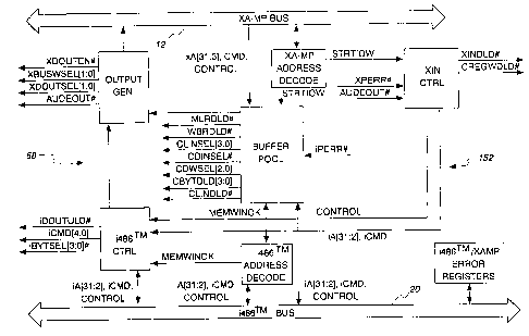
Fig. 9 is block diagram of an I/O bridge;
Fig. 10 is a block diagram of a bridge bus interface controller;
Fig. 11 is a block diagram of a bridge cache;
Fig. 12 is a block diagram of a bridge interface controller for a
write request;
Fig. 13 is a block diagram of a bridge interface controller for a read
request;
Fig. 14 is a block diagram of a bridge controller for a bus window;
Fig. 15 is a block diagram of a bridge interface register data path;
Fig. 16 is a block diagram of a bridge interface controller and
snoop;
Fig. 17 is a flow chart of snooping on a write request;
Fig. 18 is a flow chart of snooping on a read request;
Fig. 19 is a block diagram of a personal computer;
VLS:jj
CA 02215701 1997-10-17
-3-
Fig. 20 is a block diagram of a processor functional unit;
Fig. 21 is a block diagram of a memory bus controller;
Fig. 22 is a block diagram of a memory bus controller control
structure; and,
Fig. 23 is a block diagram of a processor data path.
DESCRIPTION OF A PREFERRED EMBODIMENT
A. Introduction
The following will present a detailed description of a system
implementing a presently preferred embodiment of the present invention,
starting
with a brief summary overview of the system and progressing to detailed
descriptions of each of the major functional units of the system. Each
description
of a major functional unit of the system will, in turn, begin with a block
diagram
level description of the functional unit, including descriptions of the
interstructural
and interoperational relationships of the functional unit with other
functional units
of the system. The block diagram level discussion of a functional unit will be
followed by further discussions of certain selected functions and operations
of the
functional unit.
VLS:jJ
CA 02215701 1997-10-17
-4-
Each description will be accompanied by drawings to illustrate the
corresponding portion of the description, but it should be noted that each
drawing
will focus particularly on the corresponding description and a given drawing
may
not show all elements of the functional unit, although all significant
elements of
' each functional unit will be illustrated in a drawing related to the
description of the
functional unit.
1. Description of a System 10
Referring to Fig. 1, therein is represented a general block diagram
of a symmetric mufti-processing System 10 incorporating and implementing the
present invention. As indicated therein, System 10 includes an Extended
Architecture-Multiple Processor (XA-MP) Bus 12 which interconnects a plurality
of system functional units. The system functional units include one or more
Memory Modules (Ivllvis) 14 for storing data and programs for controlling
operations of the system and operations on the data, one or more Processor
Modules (PMs) 16 responsive to the instructions of the programs for performing
the operations directed by the programs, and one or more Bridge Modules (BMs)
18 for interconnecting XA-MP Bus 12 and the system functional units with other
Alternate System (AS) Buses 20 connecting to other elements of the system. AS
Buses 20 may include, for example, the Intel i486 bus and EISA and MCA buses.
AS Buses 20 may in turn interconnect to other System Elements 22, such as
processing elements and memories, for example, microprocessors such as Intel
i486 microprocessors, and devices such as input/output (I/O) Devices 24, which
may include disk drives, keyboards, communications controllers, and visual
display generators such as graphics adapters.
As indicated in Fig. 1 and as will be discussed in the following,
XA-MP Bus 12 is comprised of either one or two Data Buses 26 for transporting
data, an Address (ADDR) Bus 28 for transporting memory and I/O space
addresses and slice information and a Command (CMD) Bus 30 for transporting
commands indicating bus related operations to be performed by the system units
connected from XA-MP Bus 12. Also associated with XA-MP Bus 12 is a
plurality of Arbitration (ARB) Lines 32 which are used by the system
functional
CA 02215701 1997-10-17
-$-
units to arbitrate among themselves for access to XA-MP Bus 12, as well as for
other operations described in the following, Interrupt (IN'I~ Lines 34 which
are
used in interrupt operations, and a number of control lines (CNTL) 35 which
will
be discussed as necessary in the following. It should be noted that all lines
of
XA-MP Bus 12 and all control lines associated with XA-MP Bus 12 are
registered, or latched, at both ends and that all bus operations are executed
with
respect to only latched data and signals.
As will also be discussed, the Data Buses 26 of XA-MP Bus 12 are
operationally separate from and independent from the ADDR 28 and CMD 30
Buses of XA-MP Bus 12 and the primary mode of information transfer over XA-
MP Bus 12, that is, for reads from MMs 14, is in the form of ordered
transfers.
In addition, the two Data Buses 26 are operationally independent from each
other
and each may execute a transfer independently of the other.
In ordered transfers, each functional unit tracks its own memory
requests through operation of an ordered request queue in each functional
unit, and
the usual sequence of handshaking operations between an information requester
and an information provided is eliminated, thereby enhancing the speed with
which
memory reads may be performed. XA-MP Bus 12 is also capable of operating in
an out-of order mode wherein the operations of Data Buses 26 are coupled with
the operations of ADDR 28 and CHID 30 Buses to perform out-of-order transfers
requiring handshaking between the requester and the provider.
Each system functional unit connected to XA-MP Bus 12 is
comprised of a set of operational elements for performing the operations to be
performed by the corresponding type of functional unit. These operational
elements will include a bus interface contml unit connected to the ADDR Bus 28
and CMD Bus 30 of XA-MP Bus 12 for controlling operations of the functional
unit with respect to XA-MP Bus 12 and a two bus interface data path units,
each
connected to one of the Data Buses 26, for transporting data between the
functional unit's operational elements and XA-MP Bus 12. In alternate
implementations of System 10, XA-MP Bus 12 may include, or may use, only a
CA 02215701 1997-10-17
-6-
single Data Bus 26 and the functional units will accordingly include, or use,
only a
single data path connecting to the single Data Bus 26.
In the instance of a MM 14, for example, the operational elements
are comprised of Memory Storage Elements (MSE) 36 which, for example, may
be comprised of column and row array's dynamic random access memories
(DRAMs) constructed as Single In-Line Memory Modules (SIIvviM) integrated
circuits such as are commonly used for such memories. The memory bus
interface control unit is comprised of Memory Controller (MC) 38 while the
memory data path unit is comprised of a pair of Memory Data Paths (IvIDPs) 40,
one connected to each Data Bus 26. In the instance of an implementation
wherein
XA-MP Bus 12 includes a single Data Bus 26, an MM 14 will correspondingly
include a single MDP 40.
In the case of a PM 16, the operational elements are comprised of
one or more Processor Units 42, each of which may have an internal, primary
cache and an associated Cache Mechanism (CM) 44, each of which may in turn be
comprised of a Secondary Cache (SC) 46 and a Cache Directory and Controller
(CD) 48. There is a PM 16 bus interface control unit for each Processor Unit
42,
represented as an Memory Bus Controller (MBC) 50, and a data path unit
comprised of one or more Processor Data Paths (PDPs) 52 for each Processor
Unit 42, the number of PDPs 52 associated with each Processor Unit 42 again
depending upon the number of Data Buses 26 XA-MP Bus 12. As indicated, each
PM 16 further includes one or more Advanced Processor Interrupt controllers
(APICs) 54 connected from INT Lines 34 for handling intel-rupt operations for
the
Processor Units 42.
Finally, in the instance of a BM 18, the Operational Elements (OEs)
56 are dependent upon the type of operations that the BM 18 is to support and
may, for example, comprise a set of bus interface logic for interfacing with
various types of AS Bus 20 or operational elements for specific purposes. In a
BM 18, the bus interface control unit is comprised of one or more Advanced Bus
Interface Controllers (ABICs) 58, which perform essentially the same type of
functions as MBCs 50. There is a bus interface data unit associated with each
bus
CA 02215701 1997-10-17
_ 7 _
interface control unit and each bus interface data unit is comprised of one or
more
Data Bus Interface Controllers (DBICs) 60, again dependent upon the number of
Data Buses 26, which form essentially the same type of functions as PDPs 52
and
MDPs 40. In addition, the DBIC 60 has an internal data cache. Each BM 18 will
also include an APIC 54 to handle internlpt operations.
2. Summary of Certain System 10 Architectural Features
As described above, System 10 is a symmetric multiprocessing
system wherein processes may be executed in any of a plurality of, Processing
Units 42 under the control of programs stored in Memory Modules 14. As will be
summarized below, and as will be described in detail in following portions of
the
present description, the system presents a unified operating environment for
executing multiple processes concurrently, while many system functions are
distributed through the functional units of the system, rather than
centralized in a
functional unit.
For example, System 10 provides a unified environment by
performing all operations within a single address space wherein all data,
program
and information storage functions of the system occupy that single address
space.
Such data, program and information storage functions may include, for example,
the memory space of MMs 14, the registers of Processor Units 42, and other
information storage functions, such as the display memories of video
controllers
and I/O devices, and the space required to store operating systems and BIOSs,
such as the ROM BIOSs commonly used in personal computers.
The management of information storage, however, is generally
distributed among the functional units of the system, so that, for example,
MMs
14 are responsible for managing the address locations within that address
space
that are used by MSEs 36 to store data and programs. In a like manner, the PMs
16 are functionally responsible for managing the address space locations
occupied
by the registers of Processing Units 42 while BMs 18 are responsible for
managing the address space locations used by video display controllers and
occupied by Read Only Memories and other memories for storing such programs
and data as ROM BIOSs.
CA 02215701 1997-10-17
_ g _
The management of the single system address space is essentially
performed by the mapping of the various storage means, such as the processor
registers, the physical memory locations in MMs 14, and such storage as is
provided in ROMs for ROM BIOSs and as video memory for video display
controllers, into the address space. In System 10, each functional unit is
therefore
responsible for mapping its associated storage spaces into the single system
address space.
To illustrate the distributed management of the system address
space, each Processing Unit 42 has a block of registers associated with it for
storing control information relating to bus operations. In System 10, however,
these registers are addressed as part of the system-wide single address space.
To accomplish this, each processor has a register associated with it
for storing a pointer which is essentially an offset address representing the
starting
address of a first register of the block of registers in the system address
space. At
system initialization each processing unit, and each functional unit in the
system,
determines its location, or "slice" number on XA-MP Bus 12, each functional
unit
being referred to herein as a "slice" in reference to its location on XA-MP
Bus 12.
As will be described further in a following description of System 10's
arbitration
mechanism, the slice numbers of the functional units are used to determine the
relative priorities of the functional units for XA-MP Bus 12 accesses and are
determined at system initialization through operation of the System 10
arbitration
mechanism.
The slice numbers are then used to determine the offset pointer
values for each block of registers and those values are stored in the
associated
register for use in addressing the registers of the blocks, with the blocks of
registers usually being assigned address space locations high in the address
space
of the system to avoid conflict with the address space assigned to system
memory
in the MMs 14.
As will be described certain of this slice number information may be
provided to other functional units of the system for use in their mapping of
their
addressable memory or storage areas into the system address space. For
example,
CA 02215701 1997-10-17
-9-
the slice numbers are provided from the processing unit functional units to
the
MMs 14 and are used by the MM 14s, in a manner described in a following
discussion of MMs 14, to constrict as address translation table for converting
system address space addresses into physical address locations of the SlIvINI
memory chips in the memories.
Similar processes are followed for each functional unit having
addressable storage or memory space associated with it and related to bus
operations, with- each functional unit mapping its associated storage, or
memory
space into the system address space. Each functional unit is thereafter
responsible
for detecting addresses on XA-MP Bus 12 which refer to memory or storage
address locations in or associated with that functional unit and responding
appropriately.
In a like manner, each functional unit of the system is responsible
for management of all information residing in its storage spaces, such as data
and
program instructions. This aspect of the distributed functionality of the
system is
particularly significant with respect to cached information as each functional
unit,
except the MMs 14, is provided with a cache mechanism for storing information
which is used by or operated upon by the functional unit. A PM 16, therefore
is
provided with one or more caches, depending upon the number of Processing
Units 42 residing therein, for storing program instructions to control
operations of
the Processing Units 42 and data to be operated upon by the Processing Units
42.
In a similar manner, BMs 18, which are primarily input/output units for System
10, are provided with caches for information being transferned between the
functional units connected from XA-MP Bus 12 and buses or devices connected
from the BMs 18.
To further illustrate the distribution of system functions among the
functional units of the system, it is well known in symmetric multiprocessor
systems that a process may execute on any processor of the system and that a
process may be assigned to a processor, begin execution, cease execution, for
example, by the end of the process's processor time slice, and later resume
execution on another processor of the system. In System 10, a process will be
CA 02215701 1997-10-17
-10-
assigned to a Processing Unit 42 and will begin execution in the Processing
Unit
42 with data and instructions belonging to the process being read from MMs 14
to
the cache mechanism associated with the initial Processing Unit 42, so that
the
data and instructions encached in the cache mechanism then "belong to" the
functional unit in which the process is executing, that is, to the Processor
42 and
associated cache mechanism. If the process is subsequently "switched" out of
the
initial Processing Unit 42, as just described, the process' data and
instnlctions
which were encached in the Initial Processing Unit 42 will remain in residence
in
the cache mechanism of the initial Processing Unit 42 and will continue to
"belong
to" the initial Processing Unit unless there is reason, such as lack of cache
memory space, for the Processing Unit 42 to transfer the data and instnlcdons
back to memory.
If the process then resumes execution on another Processing Unit
42, the process will request the instructions and data required for the
process to
I S execute and will, as described in detail below, place a request for the
data or
instnactions on XA-MP Bus 12. The sequence of events that will then be
executed
will depend upon whether the data originally read from memory had been
modified and, as will be described in greater detail in following portions of
this
description, only one valid copy of data is allowed to exist in System 10 at
any
time.
If the data originally read from memory to the cache mechanism of
the initial Processing Unit 42 had not been modified, and as such had not been
marked as modified in the cache mechanism, the valid copy is assumed to be the
copy residing in memory and is read from memory to the cache mechanism of the
Processor Unit 42 on which the process is now executing. If the data had been
modified and is resident in the cache mechanism of the original Processing
Unit 42
as marked as modified, then this modified copy of the data is the only valid
copy
of~the data and "belongs to" the original Processing Unit 42. As will be
described
further in the following, each functional unit of System 10 monitors all road
requests appearing on XA-MP Bus 12, in a process roferrod to as "snooping",
and
the original Processing Unit 42 will thereby detect the data read request
placed on
CA 02215701 1997-10-17
-11-
XA-MP Bus 12 by the new Processing Unit 42, as will any other functional unit
which contains a "shared" copy of the data.
As described below in the detailed description of XA-MP Bus 12,
and other portions of the description of System 10, any functional unit having
a
copy of requested data will detect a request for the data on XA-MP Bus 12 and
may acknowledge the request, which in systems of the prior art would comprise
an
acknowledgment that the acknowledging unit will respond by providing the
requested data. In system 10, however, a functional unit having.~~a,modified
copy
of the data, such as the original Processing Units 42, will assert a Memory
Cycle
Inhibit (MCI) and CDM command which will cancel the read operation in memory
and inform the requesting functional unit that the data will be provided from
a
source other than the memory. The functional unit having the valid copy of the
data, that is, the modified copy of the data will then arbitrate for XA-MP Bus
12
and will provide the modified copy of the data to the new Processing Unit 42
through an out-of order transfer. The Processing Unit 42 receiving the
modified
copy of the data from the originally owning Processing Unit 42 becomes the
"owner" of the data and assumes responsibility for managing that data at the
time
of the response.
Other examples of the distribution of system functions among the
functional elements of System 10 which will be described in detail in the
following
include the arbitration of XA-MP Bus 12 access among the functional units, the
execution of in-order reads from memory wherein each functional unit
requesting a
memory read is responsible for tracking its own read requests and detecting
and
responding to the corresponding memory response, and the adaptive timing of
memory operations dependent upon the type of SIIvvIM modules, bus transfer
rates,
and other factors.
Having described the general stnlcture and operation of a System 10
implementing the present invention, the following will describe the functional
units
of System 10 in further detail.
B. Detailed Description of a System 10
1. XA-MP Bus 12
CA 02215701 1997-10-17
-12-
Referring again to Fig. 1, XA-MP Bus 12 was described as being
comprised of either one or two Data Buses 26 for transporting data, an Address
(ADDR) Bus 28 for transporting memory space addresses and to a Command
(CMD) Bus 30 for transporting commands indicating bus related operations to be
S performed by the system units connected from XA-MP Bus 14. As also
described, a plurality of Arbitration (ARB) Lines 32 are associated with XA-MP
Bus 12 and are used by the system functional units to arbitrate among
themselves
for access to XA-MP Bus 12, as well as for other operations described in the
following. Also associated with XA-MP Bus 12 are Interrupt (INT) Lines 34,
which are used in interrupt operations and Control (CNTL) Lines 35.
It should be noted for purposes of the following discussions that the
primary data element used in System 10 is a block of data, or instructions,
referred to as a cache line because information, that is, data or
instructions, is
encached in System 10's caches in units referred to as lines wherein each line
occupies one address location in a cache memory.
Each cache line contains 256 bits, or 32 bytes, of information and
each Data Bus 26 is 64 bits, or 8 bytes, wide so that the transfer of one
cache line
over a Data Bus 26 requires four bus clock cycles for the actual data
transfer. In
addition, a standard head from memory is comprised of a cache line, that is, a
single read request to memory will result in a cache line of 32 bytes being
transferred over XA-MP Bus 12 to the requester, thereby requiring four
transfers
of the bus.
Each XA-MP Bus 12 operation further requires a bus clock cycle,
to switch between "bus owners". That is, a single bus clock Cyclades required
for
control of XA-MP Bus 12 to be transferred from a functional unit which is
currently using the bus to execute an operation and to a next functional unit
which
has acquired access to the bus for a next bus operation.
As will be described in the following with respect to MMs 14,
MSEs 36 of each MM 14 are organized as dual columns of address locations,
wherein one column contains even address locations and the other column
contains
odd address locations and wherein each column stores 64 bits of information.
CA 02215701 1997-10-17
-13-
MMs 14 are thereby internally organized as half cache lines, with each row
across
the two columns comprising a half cache line of 128 bits so that a single read
operation from a single row across the two columns of SI1VVIM circuits will
provide
a half cache line of information. The MM 14 to system address space mapping is
preferably structured so trat consecutive half cache lines are stored in
different
groups of SIIvvIM circuits so that two consecutive half cache lines may be
read
from MMs 14 using different memory RAS (Row Address Strobe) signals, and
thus different RAS driver circuits, thereby eliminating additional access
delay
times when using 80ns SIIViNts.
As described above, in the presently preferred embodiment of
System 10, XA-MP Bus 12 is provided with two Data Buses 26, each of 64 bits,
or one half cache line, in width, to enhance the speed of information transfer
over
the bus.
As has been described, the two Data Buses 26 operate independently
of each other. Either of Data Buses 26 may be used to perform a bus data
transfer, such as a read from memory, wherein a bus data transfer will be
completely performed upon one or the other of Data Buses 26, so that two bus
transfers may be performed concurrently, one on one Data Bus 26 and the other
on the other Data Bus 26.
A single, "standard" XA-MP Bus 12 operation, such as a cache line
read from memory, thereby requires five bus clock cycles, one for the
transmitting
functional unit to take control of the bus and four for the transfer of data
over one
of the two Data Buses 26. It should also be noted, as described in the
detailed
descriptions of XA-NiP Bus 12 and MMs 14, that System 10 may. also perform
single bus word transfers, and that a transfer may start with either an even
or an
odd cache line address, that is, is not limited to even-odd-even-odd and so
on.
As has been mentioned above, the Data Buses 26 of XA-MP Bus 12
are operationally separate from and independent from the ADDR 28 and ClvID 30
Buses of XA-MP Bus 12 and that information transfers over XA-MP Bus 12 for
reads from MNis 14, are in the form of ordered transfers wherein the responses
to
read requests are fulfilled in the order made. In in-order read operations,
the
CA 02215701 1997-10-17
-14-
responses may occur a number of bus cycles after the request was accepted by
the
functional unit which accepted the request for response, depending upon
whether
there were other requests enqueued for response. This type of operation is
referred to as "split cycle" operation as the response may be removed in time
from
the request.
In ordered transfers in System 10, each functional unit tracks its
own memory requests independently of other functional unit memory requests,
through operation of an ordered request queue in each functional unit. The
ordered request queue allows a functional unit to track both its own requests
for
memory reads and all ordered transfers from the memory, both to itself and to
other functional units, and to detect when an in-order transfer from memory is
provided in response to one of its requests occurs. A functional unit will
then
respond accordingly by accepting the data from XA-MP Bus 12. The usual
sequence of handshaking operations executed between an information requester
and
an information provider in conventional buses is thereby eliminated during the
response portion of an in-order read cycle.
In the out-of-order mode, the operations of Data Buses 26 is
coupled with the operations of ADDR 28 and ClviD 30 Buses to perform out-of-
order transfers requiring handshaking between the requester and the provider.
In
such out-of order transfers, the unit providing the information in response to
a
request does not necessarily do so in the same sequence in which the requests
were
placed on XA-MP Bus 12 and the information provider must accordingly note the
address, that is, the slice number of the unit making the request. The unit
providing the requested information will then, in effect, couple together the
operations of a Data Bus 26 with ADDR Bus 28 and CMD Bus 30 by placing the
slice number of the requesting unit, that is, the unit which is to receive the
information, on ADDR Bus 28 and an appropriate command on CMD Bus 30
while placing the data on a Data Bus 26. The receiving unit will then respond
to
the slice address and command to accept the data.
As will be described, requests for data reads from memory are
placed on XA-MP Bus 12 as ordered requests. If the data is to be provided from
CA 02215701 2000-12-11
sECT~o~~ ~ coR~~crcor~
SEE CER w iFI~~ATE
CoR~ECTIOr~ -aH~ ~c~- 3
- 15-
VO(R GERTIFIGAT
a unit other than the memory, as in the previous example wherein information
was
returned from a cache mechanism of a processor unit rather than from the
memory,
~ the unit containing the information will respond by cancelling the memory
operation,
as described, and will respond with an out-of order response. 'fo do so, the
responding unit must obtain the address, or slice number, of the requesting
unit and
does so by obtaining the slice number of the requesting unit from the bus
arbitration
mechanism rather than from the requesting unit, so that the requesting unit
does not
have to provide a self identifying address with each request. Each information
read
request may therefore be originally generated by the requesting unit as an
ordered
request and the requesting unit does not have to know beforehand how the
request will
be fulfilled.
As described, ordered operations are used for cache line and bus word reads
5 from memory, which comprise the majority of read operations in System 10.
Out-of
order operations are used for cache to cache transfers, word transfers, and
l/O
operations tluough BMs 18, thereby optimizing the operation of XA-MP Bus 12
for
each type of operation.
It should be noted that Processing Units 42 are Intel 1'entiutn processors,
the
2U associated primacy and secondary cache integrated circuits are available
from Intel, as
is the Intel interrupt processor referred to as the Advanced Processor
Interrupt
Controller. These elements are available from the Intel Corporation, as is
well known
in the art, and are fully described in the Intel tecluiical and product
manuals.
2. Memory Modules 14
25 a. Description of Memory Controller 38
As has been described, each MM 14 is comprised of an MSE 3G, which
is a row and column array of memory circuits, such as SIMM modules, for
addressably storing and providing data as is well known in the apt. Each MM 14
CA 02215701 1997-10-17
- 16-
further includes an MC 38 providing control functions for the MM 14 and one or
more MDPs 40 forming the data paths between the MSE 36 and XA-MP Bus 12,
with each MDP 40 connecting to one of the Data Buses 26.
Referring to Figs. 2 and 3, therein are respectively shown block
diagrams of an MC 38 and MDP 40.,'Referrng first to Fig. 2, the primary
interface between an MC 38 and XA-MP Bus 12 and the control lines associated
with bus operations is provided by an XAMP Control Interface (XAMPCI) 62 and
a Command Address Input Block (CMDAI) 64.
XAMPCI 62 interfaces with certain of the control lines associated
with XA-MP Bus 12 operations, which are described in detail in a following
detailed description of MC 38. As indicated in Fig. 2, input signals to RAMP
Interface 62 from XA-MP Bus 12 include nine ARB signals lines of the system
arbitration mechanism (ARB) and a Command Strobe (CSC indicating the present
of a command on CMD 30.
Output signals from XANIPCI 62 include ACK and NAK signals, a
CAE# signal indicating that a command or address received by the memory is in
error. DSO# and DS1# are individual data strobe signals for the two Data Buses
26 and ORDO# and ORD 1 # are individual signal for the two Data Buses 26
indicating that an ordered response is present upon the Data Bus 26
corresponding
to the ORD# signal.
As indicated, XAMPCI 62 provides a Local Response output to a
memory command FIFO (First In-First Out Memory), described below, indicating
that an operation request has been received that will be responded to by the
memory. XAMPCI 62 also provides a number of outputs to MDP 40, including
BINO# and BIN1# which each correspond to one of the Data Buses 26 and are
used to enable the transfer of data from the corresponding Data Buses 26 to
MDP
40. BOLJT'0# and BOiJTI # each correspond to one of the Data Buses 26 and are
signals used to enable the transfer of data from the memory to the
corresponding
Data Bus 26. BACKO# and BACK1# each correspond to one of the Data Buses
26 and are signals representing to MDP 40 that a write cycles on the
CA 02215701 1997-10-17
-17-
corresponding Data Bus 26 is validly acknowledged and not aborted, for
example,
by MCI.
CMDAI 64 interfaces with ADDR Bus 28 and Command Bus 30 to
receive and provide addresses and commands and with other bus operation
control
lines which are described in detail in a following detailed description of
MC38.
Inputs to CMDAI 64 include the addresses appearing on ADDR Bus 28, the
command signals (CMD) from CMD Bus 30, and a command strobe signal CS#
indicating that a command is present on CMD Bus 30. The (AP) and (CP) inputs
are respectively address and command parity bits. Signal BUSL# is a bus
control
line input indicating that the requesting functional unit has Locked, that is,
taken
control of, XA-MP Bus 12 for an extended period.
As represented in Fig. 2, CMDAI 64 provides outputs to the
memory command FIFO mentioned above for storage therein, the outputs
including the addresses and commands of memory requests and certain control
1 S bits. CMDAI 64 also provides Hit and Error output to XAMPCI 62 to indicate
when, respectively, received memory requests are valid or invalid, for certain
reasons.
It is indicated in Fig. 2 that MC 38 has a further interface to XA-
MP Bus 12 and the associated bus operation control lines through an Exception
Control (EXCEPT) 66 which is provided to handle exception and error
conditions.
EXCEPT 66 will not be described further at this point, but is described in the
detail in the detailed description of MC 38. MC 38 also includes a Scan
Control
(SCAM 65, which also will be described in the detailed description of MC 38.
Memory operation requests are pipelined in MC 38 through
operation of a Memory Control FIFO (MC FIFO) 68 mentioned above. As
indicated, MC FIFO 68 receives address, command and response inputs from
CMDAI 64 and XAMPCI 62, which define memory operations to be performed
and stores these operations to be operated upon in the order received.
Other inputs are provided to MD FIFO 68 from MDP 40 and
include MDPEO# and MDPEI# bus control signals indicating the presence of a
panty error detected on the corresponding Data Bus 26 by MDP 40. A (Memory
CA 02215701 1997-10-17
-18-
Cycle Inhibit) MCI# signal indicating that a current memory operation has been
cancelled, as previously described, and Cache Data Modified (CDM#) and Cache
Data Shared (CDS#) signals indicated that the presence of a modified or shared
copy of the requested data has been indicated in another functional unit and
that
the current memory cycle is canceled. ' The ACK# and NAK# signals respectively
indicate that MC 38 has accepted or not accepted a current memory operation,
while Command or Address Error (CAE#) indicates that MC 38 has detected a
command or address error.
MC FIFO 68 and EXCEPT 66 each have control signal interfaces
with an MC MANAGER 70, which provides basic control and management
functions for memory operations. As indicated, MC MANAGER 70 receives
request signal FREQUEST from MC FIFO 68 indicating the present of a pending
request and in return provides an FGRANT signal indicating that the request
may
be executed. MC MANAGER 70 concurrently provides an EGRANT signal to
EXCEPTION 66 indicating the request may be executed and receives an
EREQLTEST indicating the presence of a pending request.
As a result of these signals, MC MANAGER 70 then provides
control outputs to a DRAM CONTROLLER 72 to be used by DRAM
CONTROLLER 72 in controlling the generation of addresses (ADDR), Row
Address Strobes (RASs), Column Address Strobes (CASs) and Write Enable (WE)
signals to the MSEs 36 of the MMs 14. As is common, MSEs 36 are comprised
of dynamic random access memories (DRAMs) physically constnlcted as SI1VIM
modules.
Other inputs to DRAM CONTROLLER 72 include address, cycle
and lane control signals provided from MC FIFO 68 or from EXCEPTION 66
which, as described in detail in the detailed description of MMs 14 are
essentially
addressing information derived from the request address and command
information
stored in MC FIFO 68.
As shown in Fig. 2, MC 38 includes a Visible Register Block
(VRB) 74 having inputs from MC FIFO 38, EXCF.PTTON 66, MC Manager 70
and an MDP Interface (MDPn 76 which is comprised of registers which are
CA 02215701 1997-10-17
-19-
accessible to the system and which are used to store and provide basic control
of
error information.
MDPI 76 essentially provides a control and synchronization
interface between MC 38 and MDP 40 to control and synchronized the transfer of
S data into and out of an MM 14 through MDP 40 with the control of memory
operations by MC 38.
As indicated, these control signals exchanged between MC 38 and
MDP 40 include multi-bit MC Commands (MCMDO and MCMD1) which are
commands passed between MC 38 and MDP 40 so that each unit may request
certain operations of the other. As described in the detailed descriptions of
MC
38 and MDP 40, these commands are essentially concerned with the particularly
type of memory read or write operation to be performed, such as whether the
MSE 36 is to perform a read of a bus word or a cache line from the DRAMS of
the SIIvvIM arrays. Data lines MDATAO# and MDATAl# are used to pass data
used in MC 38/MDP 40 operations between MC 38 and MDP 40, as described in
the detailed description of MC 38 and MDP 40, and signals MGOO# and MGOI#
are used to initiate operations by MC 38 or MDP 40.
Further detailed descriptions of MC 38 may be found in Appendix
2, which is titled "Memory Controller".
b. Description of Memory Data Path 40
Referring now to Fig. 3, therein is represented a block diagram of
an MDP 40. As described, MC 38 essentially provides all timing and control
functions and signals for the MMs 14 and the memory and XA-MP Bus 12
operations performed by the MMs 14 while MDP 14 is essentially. a pipelined
data
path between XA-MP Bus 12 and the memory elements of MSE 36. As has also
been described, each MM 14 will have two MDPs 40, one connecting to each of
the Data Buses 26, and each functional unit having data connections to Data
Buses
26 will similarly each contain two similar data path elements connecting to
the two
Data Buses 26. In those implementations of System 10 using or having only one
Data Bus 26, each MM 14 will have, or will use, only one MDP 40 and each
CA 02215701 1997-10-17
-20-
other functional unit will similarly have, or use, only one data path element
to
connect to the single Data Bus 26.
MDP 40 includes an XA-MP Bus 12 Data Interface (XAMPDI) 78
to XA-MP Bus 12 and a DRAM Interface (DRMI) 80 to the DRAMS of the MSEs
S 36. As shown, XAMPDI 78 has a bidirectiorlal data interface with Data Buses
26
of XA-MP Bus 12 for transferring 64 bits of data (BD) and 8 bits of data
parity
(BDP) with XA-MP Bus 12. XAMPDI 78 further has a bidirectional Bus
Uncorrected Data Error (BUDE/1) signal line interface with a control line
associated with XA-MP Bus 12 to receive and provide a signal indicating an
uncorrected error in the data being provided to or read from the memory.
MDP 40's data interface with MSE's 36 is provided through DRMI
80 and is comprised of two bidirectional 64 bit wide data paths to and from
the
DRAMS of MSEs 36, referred to in Fig. 3 as DDO(63:0) and DD1(63:0). As has
been described, the memory elements of MSEs 36 are organized as two columns,
an even address column and an odd address column, wherein each column is one
bus word, or one quarter cache line wide. The two data buses connecting to the
MSE 36 memory elements are therefore capable of transferring a bus word in one
memory internal cycle or a single cache line in two memory internal cycles.
Associated with and parallel with each data bus to the MSEs 36, that is, with
DDO(63:0) and DD1 (63:0), are two bidirectional Error Detection and Correction
buses identified as DCO(7:0) and DC 1 (7:0) for carrying data check bits
between
the memory elements of MSEs 36 and MDP 40. In this regard, it should be noted
that the MSE's store not only the information but that row of each bus word
wide
column of the MSEs 36 also contains memory elements for storing data check
bits
associated with the corresponding bus words stored therein.
The input path from XA-MP Bus 12 extends from XAMPDI 78 to a
Write Path memory (WRITE PATH) 82, which is used to pipeline data writes into
the MSEs 36. As will be described further below, WR):TE PATH 82 also has data
path inputs from an EDAC Generator and Corrector (EDAC) 84, which in turn is
connected in the data and check bit path output from DRMI 80. As described in
CA 02215701 1997-10-17
-21-
the detailed description of MDP 40, this path is used for data write back and
correction operations.
The data path output from WRITE PATH 82 is connected to a data
path input to DRMI 80, providing the path through which information is written
into MSEs 36. The data path output from WRITE PATH 82 is also connected to
a data path input into a Write Check Bit Generator (WCBG) 86 which generates
check bits for each bus word to be written into MSEs 36 and provides the check
bits through a check bit write path input to DRMI 80 in parallel with the data
provided as bus words to be written into MSEs 36 from WRITE PATH 82.
The data word output of WRITE PATH 82 is also provided as
inputs to MDP Registers (MDPRs) 88 to allow writing of certain MDP 40
registers. The output of WRITE PATH 82 and MDPR 88 are provided as inputs
to an MC Interface (MCI) 90, which interfaces with MDPI 76, previously
described, and are used to generate the control and data signals exchanged
with
MDPI 76. As indicated, the control and data signals exchanged with MDPI 76
further include a FIFO Error signal (FIFOERO#) which indicates when there has
been an error in the FIFO comprising WRITE PATH 22 or the FIFO comprising
READ PATH 92, such as requested read operation upon an empty FIFO or a
write operation upon a full FIFO.
Next considering the data output path through MDP 40, the data and
check bits read from MSEs 36 through DRMI 80 are provided as inputs to EDAC
84, which performs error detection and correction operations and generates
corrected data bits for the bus word read from MSE's 36 and error signals SBE#
and MBE#, all of which are provided as inputs to READ PATH-92.
READ PATH 92 is essentially a FIFO for pipelining data .rids
from the MMs 14 and the data bit outputs of READ PATH 92 are provided to
XAMPDI 78 for transfer onto SA-MP Bus 12 as required.
Finally, MDP 40 includes State Machine (STATE) 94 which
controls certain operations of MDP 40. As indicated, STATE 94 receives a Bus
In (BIN#) signal from MD 38 which enables the transfer of data from XA-MP Bus
12 into MDP 40 and a Bus Out (BOUT#) signal from MC 38 which enables the
CA 02215701 1997-10-17
-22-
transfer of data from MDP 40 to XA-MP Bus 12. Other signals from MC 38
include a Bus Acknowledge signal (BACIC#) which indicates a valid acknowledged
write cycle and an Initiate (INIT) signal to initialize MDP 38. STATE 94 also
receives BDATA, MGO and MCMD from MC 38, as described further in the
~ detailed descriptions of MC 38 and MpP 40., '
Having described the overall structure and operation of an MM 14,
focusing in particular on MC 38 and MDP 40, the following will describe
certain
specific functions and operations of the MM 14.
Further detailed descriptions of MDP 40, including the features
described in the following, may be found in Appendix 3, titled "Memory Data
Path" .
3. Error Correction for Stored Data
MMs 14 perform error correction of data stored in MSEs 36 by
read-correct-wtiteback operation wherein the read-correct-writeback operations
are
performed in such a manner as not to delay the normal reading and writing of
information from and to the memory elements. In this respect, it has been
described above that MDP 40 performs error detection and correction of
information read from memory, through operation of EDAC 84 and generates
check bits for information written into memory, through operation of WCBG 86,
the check bits being written into memory and stored with the information.
When MDP 40 reads a bus word from memory and detects an error
in the data, that is, the data is in accordance with the check bits associated
with
the data, MC 38 will receive MCDE and note the address location of the data in
error being corrected through EDAC 84 for transfer to XA-MP Bus 12 and will
store this error address information (ERROR ADDR) in a Correction Queue
(CORRQ) 96.
As indicated in Fig. 4, and as has been previously described,
memory requests, that is, commands indicating operations to be performed and
addresses of information to be read or written are received from XA-MP Bus 12
by XAMPCI 62, are stored in the pipeline queue comprised of XANiPCI 62 if to
be executed by the memory, and are executed by MC 38 and MDP 40. As has
CA 02215701 1997-10-17
-23-
been described, memory read operations of bus words and cache lines are
performed as in-order operations, that is, each operation is performed in the
order
received. The operations of MC 38 and MDP 40 are coordinated through
operation of a Pending Request Queue (PREQQ) 98 maintained by MC 38 wherein
S MC 38 stores identifications of all.pending requests. MDP 40 then provides
information regarding requests as executed and provides this information to MC
38's PREQQ 98, thereby allowing MC 38 and MDP 40 to remain in
synchronization.
Associated with XAMPCI 62, CORRQ 96 and PREQQ 98 is an
Operation Arbitrator (OPARB) 100 which monitors the state of pending requests
in
XAMPCI 62 to detect when the queue of pending requests is empty. When the
queue is empty, OPARB 100 checks CORRQ 96 to determine whether the memory
has detected any storage locations containing uncorrected error and, if the
addresses of any such locations are enqueued in CORRQ 96, performs read-
correct-writeback operations. In each such operation, MDP 40 will, in
cooperation with controlling operations of MC 38, read the data from that
address
location from MSE 36 through DRMI 80, correct the data through EDAC 84 and
provide the data back through WRITE PATH 82. The data will pass through
WRITE PATH 82 to WCBG 86, where new check bits will be generated, and the
corrected data and new check bits will then be written back into MSEs 36
through
DRMI 80. In the event that OPARB 100 detects that CORRQ 96 is full, the data
correction operations will be performed as just described, but will be
performed
even if there are pending requests.
MMs 14 thereby perform error detection and correction on data
stored in the MSEs 36, but without interfering with the execution of read and
write operations, by storing identifications and locations containing errors
and
performing read-correct-writeback operations when there are no pending
requests.
Another feature of MDP 40 is illustrated by referring to Fig. 3
wherein there is represented a gated bypass data path around READ PATH 92
with control of Bypass Path Gate (BPG) 102 provided by a FIFO Etv>pT'1' signal
output of READ PATH 92. As has been described, READ PATH 92 is
CA 02215701 1997-10-17
-24-
essentially a FIFO queue wherein the information and parity bits resulting
from
read request operations are passed through the queue and to XA-MP Bus 12 in
the
order executed. In the event that all requests have been executed, the queue
will
be empty and a new request would have to pass through READ PATH 92's queue,
requiring several clock cycles, depending upon the depth of the queue, before
being available for transfer to XA-MP Bus 12. In the event the queue is empty,
however, this condition is detected by READ PATH 92 which asserts FIFO
EMPTY to BPG 102, which responds by gating the information around READ
PATH 92 and directly to XAMPDI 78 and MC 38 sends MDP 40 a BOUT signal
requesting that data to be put onto XA-MP Bus 12, thereby providing the
requested information to XA-MP Bus 12 one clock cycle sooner than would be
available through READ PATH 92.
4. Adaptive Memory Timing
MMs 14 further includes the capability of adaptively altering the
absolute and relative timing of the memory operation timing signals generated
by
MC 38 and used by MC 38 and MDP 40 in controlling memory operations in such
a manner as to adapt the operations of an MM 14 to obtain the maximum speed of
operation possible with the particular SIIVVIM circuits used in an MM 14. The
controllable signals include the SIIvvIM timing signals, including RAS, CAS
and
WE, generated by MC 38's DRAM CONTROLLER 72, together with other
timing signals generated by MC 38 and used by MC 38 and MDP 40 to control
the operations of MM 14.
Referring to Fig. 5, it is well known that SIIviNI circuits provide
coded values upon certain pin outputs which indicate at least the size and
speed of
the particular SIIvvIM circuits. In the present system, these encoded values
available through the SIIVViM circuit pins are brought out of the MM 14 MSE
36s
and are made available to MC 38. The present system further includes a Profile
Store 104, which is located in a storage location in MM 14, wherein Profile
Store
104 could contain a Profile 106 for each type of SIIVVIM group which may
appear
in MSE 36.
CA 02215701 1997-10-17
-25-
Each Profile 106 contains a set of values representing the timing
characteristics of the corresponding type of S>ZvINI module, wherein the
timing
characteristics represent the various maximum gate delays, recharge times, the
timing event intervals of the SIMNi module internal circuitry. In the present
system the timing characteristic values are not expressed in time units, such
as
nanoseconds, but are instead values representing the comparative timing
characteristics of the SIMM modules, such as counts in terms of the double
speed
clock. The timing characteristic values, however, are selected to easily
represent
the timing characteristics of both the S>M1VI modules and the basic clocks
used in
MMs 14 to generate timing signals.
At system initialization, MC 38 will read the SIIVVIM module coded
timing characteristic values provided from the SBviM module pin outputs and
will
use the coded values to select and read a corresponding Profile 106 or
Profiles 106
from Profile Store 104. The timing characteristic values are then provided to
a
TIIVViING CALCULATOR 108 in the MM 14's MC 38. TIZuvIING
CALCULATOR 108 is provided with the calculation functions necessary to
calculate the maximum time intervals required to perform each SIIVVIM
operation,
such as the maximum time which must occur between a RAS signal and a next
RAS signal, the maximum time which may occur between a write enable signal
and the result of the write enable signal, and so forth.
T)ZvIZNG CALCULATOR 108 will calculate and provide a set of
timing control values which represent the times at which timing events are to
occur in the operation of the SnvIMs, wherein each timing event is represented
by
a timing signal and the timing control values are in units of clock::periods
of the
MM 14 internal clock used to control the SIIvEvi operations. In the present
system, timing events are determined, that is, calculated, as both "absolute"
times
and as "relative" times wherein the time of occurrence of an "absolute" event
is
determined relative to a To representing the start of a memory operation cycle
and
a "relative" event is determined relative to a previous event. For example,
the
time of occurrence of the RAS and CAS signals may be determined as absolute
events relative to the To start of a memory cycle while the time of occurrence
of a
CA 02215701 1997-10-17
-26-
WE or the time at which data will appear from the SIIv>rit modules may be
determined relative to a previous event, such as the occurrence of a RAS or
CAS
signal.
The timing control values are then provided to DRAM
S CONTROLLER 72 and used by DRAM CONTROLLER 72 to generate the actual
timing signals, such as RAS, CAS and WE, to the SIIvlr~i modules.
It should be noted that in alternate embodiments of the present
invention, it- may be preferable to pre-calculate the timing values for each
profile
and to simply load the timing values to DRAM CONTROLLER 72 rather than
calculating the timing values through a TMNG CALCULATOR 108 at system
initialization.
In a present embodiment of the system, each MM 14 in the system
will use a single Profile 106, selecting the profile which matches the slowest
SnviM module contained in that particular MM 14. In alternate embodiments, it
is
possible to use multiple PROFILES 106 within a single MM 14 to accommodate
different SIMMs within an MSE 36. In this latter instance, the DRAM
CONTROLLERS 72 will store two or more sets of timing values, possible in a set
of registers associated with DRAM CONTROLLERS 72, and will select a set of
timing values dependent upon the address locations being accessed, that is,
dependent upon the type of SIIVVIM modules currently being accessed.
In a yet further embodiment of the present invention, the timing
characteristic values included in PROFILES 106 will further include timing
characteristic values reflecting the data transmission rates of Data Buses 26
0~
XA-MP Bus 12 and these values will be used in calculating the timing control
values provided to DRAM CONTROLLERs 72. In a yet further implementation,
DATA Buses 26 within a single system may have different transmission rates and
the PROFILES 106 will contain timing characteristic values for the different
bus
transfer rates. In this instance, again, DRAM CONTROLLER 72 will be
provided with and will use multiple sets of timing control values, with the
values
used during any memory cycle being dependent upon which DATA Bus 26 the
information is being written to or read fmm.
CA 02215701 2000-12-11
SECTION 8 CORRECTION
SEE CERTIFhATE
CORRECTIOP' - ARTICLE 8
VOIR CERTIFICAT
-27-
Finally, as has been described the MSEs 36 are internally organized as two
partitions, so that reads from and writes to the MSEs 36 are generally
interleaved, if
enabled, that is, to or froth alternate partitions of the MSEs 36, thereby
increasing the
overall transfer rate of data into and out of the MSEs 36. In the present
embodiment
of the system, the interleaving of memory cycles, that is, the alternation of
memory
cycles to the partitions of the MSEs 3h, are controlled by the timing
characteristic
values provided in the PROFILES 1 UG and are executed by what are effectively
two
DRAM CONTROLLERs 72, one providing the timing signals for each partition of
the
MSE 36 S1MM array. In this instance, one of the timing signals generated by
each of
the controllers is a timing signal provided to the other controller to
initiate the
memory timing cycle of the other controller, that is, a T" timing signal.
Each controller therefore determines the interval between the conclusion of
its
own timing cycle and the start of the next timing cycle, generated by the
other
I S controller, and thereby controlling the interleaving of timing cycles. The
timing cycle
initiate even generated by each controller may be calculated to occur at any
time
during the timing cycle of the controller generating the initiate event for
the other
controller, allowing any degree or period of overlap or non-overlap of the
timing
cycles, with the interleaving of timing cycles being determined by the profile
2U information.
Finally, TIMING CALCULATOR 108 arid DRAM CONTROLLER 72 are
implemented in the present implementation of System 10 as two state machines.
In a further aspect of Mms l4. the refresh cycles of the partitions, which are
controlled by DRAM CONTROLLER 72, are controlled individually and the reti~esh
25 cycles of tlae DRAMS of the pat~titiolts stay be staggered to reduce the
peak power
consumed by refresh, whirl involves reading all DRAMs of a
CA 02215701 1997-10-17
-28-
partition at a time. Refresh control bits are read in and provided to DRAM
CONTROLLER 72 to control the timing of the refersh cycles.
5. In-Order and Out-Of Order Bus Transfers
As has been described, the primary mode of information transfer
S over XA-MP Bus 12 is by in-order operations and is used for bus word and
cache
line reads from memory. A functional unit other than the memory may respond to
a request, however, as when a processor unit holds a modified copy of the
requested data in its cache, by asserting an MCI command to cancel the read
request in memory and to inform the requester that the request will be
fulfilled by
another functional unit other than the memory and by an out-of order transfer.
As described, in-order transfers are responded to by the memory in
the order in which the requests are placed on the bus and is initiated by the
requester gaining control of XA-MP Bus 12 and placing the address of the
requested information on ADDR Bus 28, together with the bus control signals.
Each functional unit tracks its own in-order memory requests, independently of
other functionals, through operation of an ordered request queue in each
functional
unit. The ordered request queue in each functional unit allows each function
to
track both its own requests for memory reads and all ordered transfers from
the
memory, whether to that functional unit or to another functional unit, to
detect
when an ordered transfer from memory appears on XA-MP Bus 12 in response to
one of its own requests. A functional unit may then respond by accepting the
data
from XA-MP Bus 12. Ordered transfers thereby eliminate the usual sequence of
handshaking operations executed between an information requester and an
information provider in the response portion of split bus operations in that
the
responder is only required to place only the requested information and bus
control
signals on XA-MP Bus 12 in the order in which the in-order requests are
received
and is not required to identify the recipient of the information further.
To briefly review and summarize the execution of in-order bus
operations as described in other sections of this description of a presently
preferred
embodiment of the invention, including the appendices which are included in
this
description, the bus interface control unit of a functional unit will place a
request
CA 02215701 1997-10-17
-29-
for information on XA-MP Bus 12 by placing the address of the information on
ADDR Bus 28, an in-order command for a bus word, cache line or double cache
line on CMD 30, and asserting the command strobe (CS). The MM 14 whose
address space contains the address of the request will recognize the request
as
' being within its address space anti will respond by accepting the request,
as
indicated by the MM 14 asserting an ACK.
If not canceled by an MCI command asserted by another functional
unit, the memory will place the request in its MC FIFO 68 queue.,to be
executed
in the order received, wherein the request information stored in MC FIFO 68
includes the type of operation requested and the address of the requested
information. If the request is canceled by an MCI command, the request will be
canceled and will not be placed in MC FIFO 68.
When the request is finally executed from MC FIFO 68, the
memory places the requested information on one of Data Buses 26 in one or more
bus transfers. The memory also asserts appropriate control signals on the bus
at
the start of the transfer, including asserting an ORD#0 or an OED#1 signal,
depending upon which of Data Buses 26 is information is being provided, and
asserting Data Strobes (DSs).
The bus interface control element of the originally requesting
functional unit will detect the occurrence of an in-order response on XA-MP
Bus
12, as it has been detecting the occurrence of all in-order responses
appearing on
XA-MP Bus 12, by monitoring the CMD Bus 30 and the ORD control lines. If
the response corresponds to an in-order request that it earlier placed on XA-
MP
Bus 12, the=functional unit will respond by accepting the information from the
Data Bus 26 that the information is being sent on and reading the information
from
the Data Bus 26 as indicated by the Data Strobes.
In the present embodiment of System 10, only the memory has an
operation queue, in MC FIFO 68, and this only the memory may contain more
than one outstanding request at a time. The functional units other than the
memory therefore require only a single register or memory in their bus
interface
control elements to store their outstanding requests. In alternate
embodiments,
CA 02215701 1997-10-17
-30-
however, each functional unit may be provided with a request queue in its bus
control interface element to store multiple outstanding requests. In this
implementation, the in-order request queue in each functional unit may be
expanded in a manner similar to the in-order request queue in each MM 14 to
provide response indications for multiple requests.
As the above operations of the bus control interfaces of the memory
and other functional units are described in detail in the structural and
operational
descriptions for each functional unit, the following will focus on the in-
order
queue in the memory and in each functional unit and the functional elements in
the
memory and in the functional units that operate with and exchange signals with
the
in-order queues will be understood by reference to the descriptions particular
to
the memory and the other functional units.
Referring now to Fig. 6, therein is presented a functional block
diagram representation of an in-order queue in a functional unit and the in-
order
queue in the memory. It should be noted that there is an in-order queue in the
bus
control interface element of each functional unit and in each MC 38 of each MM
14.
As shown, the in-order request queue residing in a functional unit is
identified as Functional Unit In-Order Queue (FUIQ) 110 while the in-order
request queue residing in an MC 38 is identified as Memory In-Order Queue
(1VIIQ) 112. Each is comprised of a request queue and a response queue,
respectively referred to as Functional Unit Request Queue (FIJREQ) 114, Memory
Request Queue (MREQ) 116, Functional Unit Response Queue (FLJRSQ) 118 and
Memory Response Queue (MRSQ) 120, wherein FUREQ 114 tracks in-order
requests submitted by the functional unit, MREQ 116 tracks in-order requests
accepted by the MIC 38 for the MM 14, FURSQ 118 tracks in-order responses
appearing on XA-MP Bus 12 from any MM 14 and MRSQ 120 tracks in-order
responses appearing on XA-MP Bus 12 from any MM 14.
Referring first to FUIQ 110, the Functional Unit Bus Control
Interface (FUBCI) 122 of the functional unit places in-order requests on XA-MP
Bus 12 as described elsewhere herein and upon placing each in-order request on
CA 02215701 1997-10-17
-31 -
XA-MP Bus 12, inserts an indication of the request (REQ) into FUREQ 114.
FUREQ 114 may, for example, be implemented as a single bit wide wrap around
shift register wherein the output is connected back to the input, so that the
requests
will rotate in the loop until fulfilled. In this implementation, the insertion
of a
request indication REQ is accomplished by placing a bit in the input of the
shift
register, such as a logic " 1 ". FUBCI 112 detects each in-order request
placed on
XA-MP Bus 12 by any functional unit and clocks FLJREQ 114 upon each
appearance of an in-order request on XA-MP Bus 12, so that the REQ indications
in FZJREQ 114 are moved along the shift register and so that the position of
any
REQ indication thereby represents the relative order of an in-order request by
that
functional unit relative to all other in-order requests made by all other
functional
units.
FL1IQ 110 tracks all in-order responses appearing on XA-MP Bus
12 through operation of FURSQ 118, which is clocked by the functional unit's
FUBCI 122 each time the FUBCI 122 detects an in-order response from an MM
14 on XANiP Bus 12. In response, FURSQ 118 generates a pointer (ORDP)
which identifies the occurrence of a current in-order response in a sequence
of
in-order responses. FIJRSQ 118 and the analogous MRSQ 120 in MIQ 112 are
represented in Fig. 6 as rotating shift registers moving along a bit which
represents a current response, but may alternately be implemented as counters
whose number output identifies, at any time, a current response in a sequence
of
responses.
The position of each REQ indication in FUREQ 114 is compared to
ORDP from FUR.SQ 118 by a COMPARE 124 and when the position of an REQ
indication is found to coincide with a current response as indicated by ORDP,
an
Own Response (OPVVNRES) output is generated to FUBCI 122 to indicate that a
current in-order response corresponds to an in-order request earlier submitted
by
the functional unit.
In summary, therefore, FURSQ 118 tracks and indicates the
sequential occurrence of in-order responses on XA-MP Bus 12 while FL1REQ 114
tracks and indicates the location or locations of the functional unit's own in-
order
CA 02215701 1997-10-17
-32-
requests in the sequence of in-order requests that have been placed on XA-MP
Bus
12, and a coincidence between FLTRSQ 118 and FUREQ 114 indicates an in-order
response corresponding to an in-order request submitted by the functional
unit.
Referring now to MIQ 112, each MM 14 is required to track its
' own in-order operations relative to in-order operations performed by all MMs
14
resident on XA-MP Bus 12 as each MM 14 will execute in-order operations
independently of the other MMs 14, with each MM 14 recognizing in-order
requests directed to its own address space and accepting and responding to the
requests.
MIQ 112 operates in much the same manner as FUIQ 110, with
MRSQ 120 tracking all in-order responses appearing on XA-MP Bus 12 in the
same manner as FURSQ 118. MREQ 116, however, tracks in the in-order
requests accepted by the MM 14 relative to all other in-order requests,
placing an
indication of a request that it has accepted (MYREQ) into MREQ 116 each time
it
accepts a request. MC 38 detects each in-order request appearing on XA-MP Bus
12 and clocks MREQ 116 each time an in-order request is accepted by any of the
MMs 14, that is, upon each occurrence of an in-order request which is not
canceled by an MCI. As represented, MREQ 116 may therefore contain several
MYREQ indications, one for each accepted by the MM 14, MREQ 116 will
thereby contain a sequence of request indications which represents the
sequence of
occurrence of each in-order request that has appeared on XA-MP Bus 12 and
wherein each request accepted by the MM 14 is represented by an MIrREQ and
each request accepted by another MM 14 is represented by another indication,
such as a logic "0" .
In a manner similar to FtJIQ 110, a COMPARE 124 will provide
an Own Request (OV~~NREQ) output when there is a coincidence between an
ORDP output of MRSQ 120 and a MYREQ from MREQ 116, thereby indicating
that the MM 14 is to execute the corresponding in-order request stored in its
MC
FIFO 68 as the coincidence indicates that this was the next in-order request
accepted by the MM 14s of System 10. MC 38 of the MM 14 will respond to the
OV~NREQ by executing that request.
CA 02215701 1997-10-17
-33-
Further description of the operation and execution of in-order and
out-of-order operations will be found in other sections of the description,
including
the appendices which are a part of this description of System 10.
6. Address Space Mapping
As described previously, System 10 provides a unified environment
by performing all operations within a single address space wherein all data,
program and information storage functions of the system taht are related to
bus
operations occupy that single address space. Such information storage
functions
may include, for example, the memory space in MMs 14, registers of Processor
Units 42, and other information storage functions, such as the display
memories of
video controllers and I/O devices, and the space required to store operating
systems and BIOSs, such as the ROM BIOSs commonly used in personal
computers.
The management of bus related information storage, however, is
distributed among the functional units of the system, so that, for example,
MMs
14 are responsible for managing the address locations within that address
space
that are used by MSEs 36 to store data and programs. In a like manner, the PMs
16 are functionally responsible for managing the address space locations
occupied
by the bus related registers of PMs 16 while BMs 18 are responsible for
managing
the address space locations used by video display controllers and occupied by
Read
Only Memories an other memories for storing such programs and data as ROM
BIOSs.
Tfie management of the single system address space is essentially
performed by the mapping of the various storage means, such as the PM 16
registers, the physical memory locations in MMs 14, and such storage as is
provided in ROMs for ROM BIOSs and as video memory for video display
controllers, into the address space. In System 10, each functional unit is
therefore
responsible for mapping its bus operation related storage spaces into the
single
system address space. An example of this mapping has been discussed previously
with regard to the mapping of the PM 16 registers into the system address
space.
CA 02215701 1997-10-17
-34-
This process is functionally and diagramically illustrated with the
aid of Fig. 7, which illustrates the basic mapping function performed in each
functional unit. It will be appreciated that the functions described herein
may be
performed in a number of ways, such as through memory resident tables or
through programmed gate array, but that the basic function performed will be
essentially the same for each implementation.
Fig. 7 shows the use of an Address Space Map (ASMP) 126 in a
functional unit~to map and relate system memory space addresses,appearing on
XA-MP Bus 12 (RAMP ADDRs) into the memory and storage space or spaces in
each functional unit, indicated in Fig. 7 as Functional Units Memory Space
(FIJMS) 128.
As indicated, each FUMS 128 may be organized or partitioned into
Memory Space Sub-Spaces (MSSS) 130 which may in turn represent contiguous
areas within a single memory space, as in the MSEs 36 of the MMs 14, or
individual locations within the memory and storage spaces of or accessible to
the
functional unit, such as individual ROMs for ROM BIOSs and video memories for
video display controllers.
ADMP 126 contains a Map Entry (MPE) 132 for each MSSS 130 of
the. functional units memory space wherein each MPE 132 also corresponds to an
address or range or addresses in the system address space as represented by
the
XAMP ADDR addresses.
The information contained in each MPE 132 may depend upon the
particular. functional unit for which the address space mapping is being
performed,
but will most often at least contain at least a bit represented as bits 134
which
indicates that the functional unit contains a memory space (MSSSO 130
corresponding to the corresponding XANIP ADDR address or range of addresses.
Bit 134 would be used, for example, in MMs 14 to detect that the MM 14
contains a memory space containing the~information indicated by an address
provided on XA-MP Bus 12 as part of a memory read request.
Continuing with this example, each MPE 132 may contain further
bits or fields that would contain information identifying the row, column and
CA 02215701 1997-10-17
-35-
group of SIlv>r~I modules containing the corresponding memory locations.
Therefore, in addition to quickly identifying whether an address location
resides in
a given MM 14, the information from the MPE 132 would, with equal speed,
translate the address given in the memory request on XA-MP Bus 12 into a
physical location in the SIIv>Ivi modules by concurrently providing the row,
column
and group numbers of the SIIvviM modules containing the addressed information
and this information can be provided to DRAM CONTROLLER 72 so that a
corresponding read operation from the addressed locations in the SIIVVIM
modules
can be performed without further delay.
In a further example of the address space mapping provided in the
functional units of System 10, it may be desirable to offset the address
allocations
of MSSSs 130 relative to the system address space. An example of such may be
in the case of MMs 14 wherein the MMs 14 are to contain a contiguous address
space formed of the memory locations of the SIIvvIMs but wherein it is desired
to
reserve certain low addresses for specific purposes, such as for system or
processor registers. In this instance, the functional units outside of MMs 14
would contain registers identifying the address locations to be reserved and
the
MPEs 132 of the MM 14 ADMPs 126 could be entered into the ADMPs 126 in an
offset order, thereby providing an automatic offset in the system address
space to
memory location mapping performed in the MMs 14. In a similar manner, the
coded size information read from the SlluviMs may be used by the system to
generate ADMP 126 offsets for each MM 14 so that each MM 14 address space to
memory location mapping can be offset in a manner to map the individual MM 14
memory locations to form a contiguous address space.
As described, the information contained in the MPEs 134 may differ
between functional units, according to the address mapping needs of the
functional
units, an example of such being the mapping of the Processor Unit 42 registers
as
compared to the mapping of MM 14 memory locations. In other functional units,
the information may, for example, reflect whether the corresponding memory or
storage locations are cacheable or non-cacheable or read-only.
CA 02215701 1997-10-17
-36-
Finally, in the present implementation of System 10, the address
mapping for the functional units is performed either at system initialization
time or
beforehand and stored, and is loaded into the ADMPs 126 of the functional
units
at system initialization.
7. Bus Access Arbitration
As discussed previously, among the system functions which are
distributed among the functional units of the system is the contention and
arbitration of-access to XA-MP Bus 12 by the functional units of the system.
The
. n::
sole exception is MMs 14, which do not arbitrate for access to the bus.
The functional units of System 10, referred to otherwise herein as
"slices", each include arbitration logic connected to Arbitration Lines (ARB)
32 to
contend for access to XA-MP Bus 12 on a relative priority basis wherein their
respective priorities are determined by their "slice" locations along XA-MP
Bus
12.
Referring to Fig. 8, therein is shown a diagrammatic, functional
illustration of the arbitration mechanism of System 10. As has been described,
arbitration is executed through a plurality of Arbitration Lines (ARB) 32,
indicated
herein as ARB 32-0 through ARB 32-9. Each slice, or functional unit, ~of
System
10, is indicated in Fig. 8 as one of SLICEs 134-0 through 134-9, thereby
representing a system having 10 slices, or functional units. The upper portion
of
Fig. 8 illustrates the connections of the SLICES 134 to the ARB 32 lines and
the
lower portion of Fig. 8 is a functional block diagram representation of the
arbitration logic in one SLICE 134.
As indicated, the arbitration logic for each SLICE 134 includes an
Arbitration Signal Latch (ARBL) 136 having inputs connected from each ARB
Line 32, an Arbitration Mask register (ARBM) 138 also having inputs connected
from each ARB Line 32, and Arbitration Control (ARBC) 140. Each ARBC 140
is connected to the ARB Line 32 corresponding to its SLICE 134 to assert its
SLICE's own ARB signal onto its own ARB 32 line.
As is diagramically represented in Fig. 8, the connections of each
SLICE 134 to the ARB 32 lines is shifted with respect to the other SLICES 134
as
CA 02215701 1997-10-17
-37-
regard the input connections to ARBM 138. That is, each SLICE 134's ARBM
138 has an input connected from ARB 32-0, another connected from ARB 32-1,
and so on. These shifted connections are symbolically represented in Fig. 8 by
the circles represented at the intersection of one of the connections between
an
ARB Line 32 and a SLICE 134, wherein the circles indicate connection between
the ARB Line 32 and the a first bit input to the ARBM 138 latches, with the
order
of increasing higher numbered connections being indicated by the arrow
adjacent
to the circle. It will be understood that the connections to ARB Lines 32
proceed
in numeric order across the inputs of each SLICE 134, with the connections
"wrapping around" so that each of ARB Lines 32 is connected to an ARBM 138
input of each of the SLICE 134. Each ARB 32 line is also connected to a input
of
ARBL 136, but through unshifted connections.
In the present implementation of System 10, the BRIDGE 56 is
usually assigned the highest priority slice with the PMs 16 occupying lower
priority slices. This assignment is not fixed, however, and any functional
unit
may be plugged into any slice location. The slice locations, and thus the
relative
priorities, of each slice will then be determined at system initialization,
wherein a
system master functional unit, usually a BRIDGE 56 will assert a logic level
upon
its ARB signal output from its ARBC 140. Because of the shifted connections
between ARB Lines 32 and the inputs of the ARBMs 138, the logic level from the
master unit will appear at successively number inputs across the ARBM 138's of
the latches and the input at which the logic level appears at the ARBM 138
inputs
of any given slice will determine the slice number, and thus the relative
priority of
that slice. The inputs from ARB Lines 32 are latched and stored in each
slice's
ARBM 138 to be subsequently used by each slice as a "mask" in determining the
time of access of the slice to XA-MP Bus 12 as described further below.
In the instance when only one slice has asserted its ARB Line 32,
that slice will gain control of XA-MP Bus 12 and no arbitration is required.
In
the instance wherein several slices assert their ARB signals during the same
bus
clock cycle, however, the slices must arbitrate among themselves to determine
which slice will have first access to the bus. In this regard, it should be
noted that
CA 02215701 1997-10-17
_ 3g__
the arbitration mechanism alternates latches ARB signals into the SRBLs 136
and
performs arbitration operations in the ARBCs 140 on every clock cycle.
If a number of slices assert their ARB signals during the same clock
cycle, those slices form a "group" which will retain control of XA-MP bus 12
among themselves by continuing to assert their ARB signals until each has
gained
access to the bus, each relinquishing access to the bus and releasing their
ARB
signal after it has executed its bus operation. The selection and sequence of
bus
accesses among the slices forming a group are performed through the "masks"
stored in each slice's ARBM 138 at system initialization. Each slice in a
group
will, at each clock cycle, compare its mask to the current ARB signals latched
in
its ARBL 136, which are latched again at each clock cycle. This operation is
usually. performed by logically ANDing the slice's mask with the currently
latched
ARB signals. If a slice's ARBC 140 finds that there is a higher priority slice
with
an ARB signal currently latched into the slice's ARBL 136, the slice yields
priority, and control of the bus, to the higher priority slice.
The slices in the group will then arbitrate among themselves at each
successive clock cycle, gaining control of the bus according to their relative
priorities as each higher priority slice completes its bus operation. Each
slice will,
upon completing its bus operation, relinquish control of the bus and cease to
assert
its ARB signal.
According to the priority arbitration rules implemented in the logic
circuitry of each slice's ARBC 140, a slice which is a member of a group and
which has either completed its bus operation and relinquished control of the
bus,
or has dropped out of its group by ceasing to assert its ARB signal; may not
attempt to assert control for the bus until every member of the group has
either
completed its respectively bus operation or has dropped out of the group by
ceasing to assert its ARB signal as a member of the group.
Further according to the arbitration rules implemented in the
ARBCs 140, no slice which is not pan of a group can assert its ARB signal or
attempt to join the group until every member of the group has either completed
its
bus operation or has dropped out of the group. The exception to this nrle is
that a
CA 02215701 1997-10-17
-39-
high priority slice may break into a group, but cannot break into two
consecutive
groups if it was NAKed out of the first group.
System 10's arbitration mechanism permits the overlap of bus access
arbitration, but not of bus access, by providing a means in ARBC 140 whereby a
slice may determine, from the ARB signals, that only one slice remains in a
group, or that only a single slice has requested access to the bus at that
time,
effectively a group with only one member. The timing through the bus line
latches at each end of each bus associated line, including the ARB 32 lines,
and
the alternate execution of ARB signal latches and access arbitration's on
successive
bus clock cycles permits a potential requester to ascertain that the ARB 32
line of
a current owner of the bus will be released on the next bus cycle and to
assert its
ARB signal during that bus cycle, so that its ARB signal will be latched into
the
ARBLs 136 of the slices at the next bus cycle. Waiting requesters may thereby
initiate the next arbitration for the bus while the last member of a previous
group
of a single possessor of the bus is completing its bus operation.
Finally, it has been previously described that certain requests for
reads of information will result not in an in-order but in an out-of-order
operation
wherein the request is canceled in memory by another functional unit's
assertion of
an MCI signal and wherein the functional unit canceling the memory operation
will thereafter fulfill the request by performing an out-of order operation.
As has
been described, in an out-of order response to a request the responding unit
will
arbitrate for access to the bus and when control of the bus is obtained,
effectively
couple together the operation of ADDR Bus 28, CMD Bus 30 and DATA Buses
26 by placing the requested information on the bus together withoa command
indicating that this is an out-of order response and the address of the
functional
unit that submitted the request.
As has also been described, a requesting functional unit does not
identify itself by transmitting its address or other identification when
making a
request for a single or multiple bus word or for a single or multiple cache
line as
the request is expected to be fulfilled as an in-order operation, as described
previously. It is necessary for the out-of-order responder to identify the
requester
CA 02215701 2000-12-11
SECTION ~ CORR~CTIQIV
SEE CERTlFhATE
CORRECTION.' -ARTICLE
VOIR CERTIFICAT
-40-
when executing the out-of order response and this is performed through the
arbitration
mechanism. 'that is, while the requester does not transmit an identification
of itself;
the requester's slice number is available at each other functional unit of the
system
and an out-of order responder which asserts an MCI to cancel the memory
operation
will read and store the requester's slice number, identified in I~ig. 8 as
Slice Nuntbcr
(SLICEN) from its ARBC 140, thereafter using that slice number as the
requester's
address when executing the out-of=order response.
8. Bridge Interface Controller 56
I U Fig. 9 presents a functional overview block diagram of the bridge interUce
controller 56 which interconnects the XA-MP bus 212 and the AS bus 2U, which
(in
the preferred embodiment) is an Intel 1486 bus identical to that which
interconnects a
conventional Intel 1486 processur and its associated RAM memory to the other
components of a standard personal computer system.
I 5 The bridge interface controller 56 can be mounted on the mother board of a
server workstation, where the AS bus~2U would connect to a conventional EISA
or
MC( PC-compatible f/0 bus and controller system of the type used in
conventional
If3M PC compatible file servers and the like. Presumably, the motherboard
would be
equipped with EISA or MCl slots for accessory cards, such as local area
network
2U adapter cards. It might also drive an SCSI bus leading to one or more hard
disk drive
systems or other type of standard disk drive controller system. See, for
example, f: IG.
l9 which presents a block diagram of a typical PC 142.
It is also contemplated that associated with the AS bus there will typically
be
standard PC support hardware, such as an interrupt controller, several direct
memory
25 access devices, and bus mastering hardware that permits accessory devices
to gain
access to and control of the AS bus 20. Most typically, direct
CA 02215701 1997-10-17
-41 -
memory access devices carrying out such tasks as disk reads and writes will,
in
response to data output commands received from the central processing units,
set
up direct memory access (DMA) reads and writes to and from the disk drives
over
the EISA or MCA bus controller and the bridge interface controller 56 to and
from the main system RAM.
With respect to FIG. 9, functionally the bridge interface controller
presents a XA-MP bus window to the AS bus 20 through which DMA controllers
and other bus masters connected to the EISA or MCI bus can address data store
and retrieval commands in precisely the same manner as if these commands were
directed to the RAM memory associated with a conventional 1486 microprocessor.
These commands pass through a sequencer 146, through the window 144, and
through a XA-MP bus interface 148 to the XA-MP bus 12, although many of these
commands can be satisfied by reference to a cache (to be described) within the
bridge interface controller 56 without any need to access the XA-MP bus 21.
The bridge interface controller also presents an i486 bus window
150 to the XA-MP bus 12 through which the multiple processors connected to the
XA-NP bus 12 can access directly anything connected to the EISA or MCA bus,
such as serial and parallel communication ports, VGA or other display
adapters,
and ROM-based program code. Such accesses are never cached but pass directly
from the XA-MP bus 21 through the interface 148 to the 1486 bus window 150
and the sequencer 146 to the AS bus 20 and to the various accessories beyond.
From a hardware point of view, the bridge interface controller is
constructed from three 1JSI chips an ABIC chip 152 (Fig. 10) and one or two
DBIC chips 154 (Fig. 11). These are connected to the busses 20:and 21 as is
illustrated in Fig. 15. Each DBIC chip 154 connects to a respective one of the
two data busses within the XA-MP bus 21, and both connect to the AS bus 20.
Both contain cache memory, and the associated address tags are contained
within
the ABIC 152. The bus address and control lines connect primarily to the ABIC
152, which contains most of the bridge control logic. The state registers 156
which define the state of the bridge interface controller are also contained
within
the ABIC 152. Since these registers must be program accessible, serial I/O
CA 02215701 1997-10-17
-42-
interfaces 158, 160, and 162 are provided whereby register values may be
serially
shifted between the DBICs 154 and the ABIC 152 over data line "0" of the AS
bus
20 so that the registers 156 can be loaded from and unloaded to the data bus
portions of the XA-MP bus 21. Figs. 11 and 12 illustrate what elements are
S present on each type of chip. The remaining. figures do not distinguish
between
the two types of chips, but consider the bridge interface controller to be a
unitary
device. An explanation of the signals seen in Figs. 11 and 12 can be found in
the
Appendices.
Fig. 12 illustrates in a functional manner those elements of the
bridge interface controller 56 that participate in the processing of data
write
requests originating from bus master or direct memory access devices residing
beyond the AS bus 20 in the EISA, ISA, or MCA or SCSI bus system.
When an AS bus write request is received by the XA-MP bus
window 144, the bridge interface controller 56 first closes the i486 bus
window
150, temporarily cutting off CPU access to the AS bus (step 162). Any pending
CPU commands (stored in a i486 command queue 164 shown in Fig. 14) are
promptly executed and cleared out (step 166). Next, the bridge interface
controller 56 releases the AS bus 20 (step 168) for use by the DMA or bus
master
or other device.
Next, if it is a write request, a cache 170 is tested to see if it
contains a cache line corresponding to the specified address (i486 snoop logic
172). The tag portion of the address presented to the window 144 is fed into
the
cache 170 and a compare signal signals to the snoop logic 172 whether the line
of
data exists within the cache 170. If the line is present, then a HIT signal
causes a
write to cache operation (step 174) to be carried out. If that is the last
byte in the
cache, and assuming that this cache line contains modified bytes (as marked by
modified bits 174 shown in Fig. 16 -- step 180 in Fig. 12), then at step 180
the
cache line is automatically written back to RAM and is freed up for use to
receive
a later incoming cache line of data, assuming a multiple byte or word transfer
is in
progress. By thus freeing up a cache line as soon as it is full of incoming
data,
the data input process is confined to two cache lines and does not overwrite
the
CA 02215701 1997-10-17
- 43 -
entire cache, thereby interfering with other input or output transfers that
may be in
progress simultaneously. The cache thus functions as if it were a buffer for
incoming memory write requests, yet behaves as an I/O cache at other times and
for the central processing units, as will be explained.
Finally, at step 182,. an optional test can be carried out to see if the
"n" th byte in the cache line (where "n" is adjustable) has been written. If
it has,
and we are nearing the end of this cache line, the controller 56 at 184
generates a
"BICL" command, which is sensed by all the other caches associated with the
multiple processors. If any of those caches contains a modified copy of the
next
sequential cache line modified, this "BILL" command causes them to write the
modified line back to RAM and to mark their cache entries "invalid" .
Likewise,
any caching unit cache that contains an unmodified copy of this next
sequential
change line mark their cache entries "invalid." This "BICL" command ("Bridge
Invalidate Cache Line" command), without the need for a data transfer, thus
sets
up the system to receive data bytes in the bridge cache. If any central
processing
unit attempts to access this same cache line while it is being loaded with
incoming
data, snoop logic 186 (Fig. 16) associated with the XA-MP bus detects that
this
cache line is marked "modified" and NAKs the memory request attempt until, at
step 188, the altered bytes are restored to RAM memory (by WBW commands,
with the memory merging the altered bytes with the remainder of the cache
line).
If the cache line is not already present within the cache 170, as
indicated by the snoop logic 172 generating a MISS, then a BICL command is
generated at 190 to insure that only RAM has an updated copy of the cache
line,
and at step 174 the incoming data is written into an empty cache line in the
cache
170, marked with its readability bit 192 (Fig. 16) set to indicate it contains
some
undefined data and with the appropriate ones of its modified bits 176 (Fig.
16) set
to indicate which are the new, incoming data bytes and which are invalid
bytes.
But if some other cache contains a modified copy of this particular cache
line, the
snoop logic 186 associated with that particular cache generates a NAK signal
(detected at 194) to give the cache unit time to return the modified value to
RAM.
The peripheral device is stalled until the BICL is accepted and the modified
value
CA 02215701 1997-10-17
has been returned to RAM. In most cases, the steps 182 and 184 will have
caused
the BICL command to go out at an earlier time, so that this NAK and the
subsequent delay will not occur.
Fig. 13 illustrates in a functional manner those elements of the
S bridge interface controller 56 that participate in the processing of data
read
requests originating from bus master or direct memory access devices residing
beyond the AS bus 20 in the EISA, ISA, or MCA or SCSI bus system.
Next, in the case of a read, a cache 170 is tested to..see if it contains
a cache line corresponding to the specified address (i486 snoop logic 172).
The
tag portion of the address presented to the window 144 is fed into the cache
170
and a compare signal signals to the snoop logic 172 whether the line of data
exists
within the cache 170.
If the cache line is present, then a HIT has occurred, and step 198
transfers the requested data from the cache to the waiting device. At step
200, if
the "n"th byte, where "n" is adjustable", has just been read, then optionally
at 202
a RCL command is issued to cause the next successive cache line of data to be
retrieved from RAM (or from some cache where it exists in modified form). If
the cache line data is not present, then a MISS occurs, and step 204 initiates
an
RCL command that retrieves the cache line from RAM memory (or from some
other cache where it has been modified). To save time, at the same time the
new
cache line is loaded into the cache it also bypasses the cache and proceeds
directly
to the requesting device over a parallel path (step 205).
Data reads and writes initiated by the multiple CPUs and directed at
devices beyond the bridge interface controller are directed to the i486 bus
window
150 shown in Fig. 14. These requests may be of two types: actual CPU I/O
requests, which require acknowledgment in the case of writes, and CPU memory
head and write requests that are to be mapped into the AS Bus 20 address space
in
some manner. The preferred embodiment, at 206 in Fig. 14, includes a variety
of
such AS Bus 20 address space mappings, including the following:
ISA compatible mapping of the lower few megabytes of RAM
memory to the memory address side of the AS bus address space, such that
blocks
CA 02215701 1997-10-17
- 45 -
of memory in 4K, 16K, 64K, and 1 Meg sizes can be marked read only (read AS
bus, write to RAM), write only (write to AS bus, read from RAM), read/write
(reads and writes to AS bus), and RAM only (no AS action). This enables ROM
to be shadowed in RAM, some RAM in AS bus space to appear amidst RAM
generally, as is required for VGA and EGA video graphics controllers, and RAM
used for shadowing to be effectively made read only. Also, access to some RAM
can be switched on and off as needed by various PC ROM BIOS programs. The
need for all of~ this will be apparent to all those skilled in the design of
IBM PC
compatible computer systems and needs not be explained here in detail.
Four relocatable windows are also provided that map very high
memory addresses (above the starting address in the base register "relowin
base")
into two 4 MB and two 8 MB windows in AS address space. This facilitates the
use of video graphics controllers without interfering with the operating
systems
which require all of the lower 16 MB of memory for their own purposes. Another
window, variable in size from 16 bytes to 4 gbytes, maps XA-MP memory
address cycles into AS bus I/O address space cycles. This window is defined by
the registers "begin-con" and "end con".
All of these AS address mappings and Read only, Write only, (etc.)
characteristics are defined by values stored within the registers 156 (Fig.
15) that
result in the AS bus address mapping 206 (Fig. 14) which causes the 1486 bus
window 150 to recognize and to intercept memory and I/O read and write
requests
addressed to the devices beyond the bridge interface controller 56 and to
intercept
those requests.
XA-MP bus accesses into the AS bus address space: are simply
accepted, ACKed and MCIed, and processed (if they are not NAKed because the
command queue 164 is full or because the i486 bus window is closed pending
action following steps 162 in Figs. 12 and 13 when a DMA or bus master data
transfer is occurring). An MCI cancels any response by normal RAM and advises
the CPU making the request that the response will be an "out of sequence"
response.
CA 02215701 1997-10-17
-46-
Up to four such requests may be queued up in the bus command
queue 164 along with the slice number of the requesting central processing
unit.
The commands are applied to the AS bus 20. When a response comes back, the
bridge controller 56 arbitrates for the main bus (and gains it quickly, since
it is
assigned the highest priority. Next, it generates an RWR command addressed to
the requesting slice and accompanied by the returned data; or, in the case of
an
I/O address space write, it simply sends out the IOWR (I/O write response)
command using only a bus address cycle and no data cycles.
For IBM-PC compatibility, some bridge interface controllers can be
designed to respond to an interrupt acknowledge command. When an i486 or
Pentium processor from among the multiprocessors acknowledges a hardware
interrupt and calls for the interrupt number, the MBC 50 generates an INTA
command which is passed to the AS i486 bus as if an i486 bus were
acknowledging an interrupt and requesting the interrupt number. The interrupt
number, returned by the EISA or MCI logic, is then passed back to the MBC 50
in the form of an RWR command with the interrupt number as data, and is
ultimately presented to the Pentium or i486 that needs it.
Bridge interface controller register access commands are processed
by step 208 as shown in Fig. 15.
9. Cache Snoop Logic
Figs. 16, 17, and 18 illustrate the structure (Fig. 16) and functional
operation (Figs. 17 and 18) of the MESI cache snooping protocol that enables
multiple CPU and bridge interface controller caches to function simultaneously
and
cooperatively in a symmetric bus caching system in which no one party ever
owns
a cache line. It thus differs from prior MOSI system (where Ownership is
replaced by Exclusive access, which means sole but not exclusive access to a
cache line).
The convention is as follows: A cache can contain no copy of a
cache line; or it can be the Exclusive (meaning only) cache to contain a
particular
cache line; or, if others also contain a copy, it can be Sharing access to a
cache
line; or, if the cache line has been altered, it is a Modified cache line and
no one
CA 02215701 1997-10-17
-47-
else can have it; or, if someone else Modifies their copy, we mark our copy
Invalid as if we did not have it, freeing the space for reuse, and sending
modified
data back to memory.
Accordingly, each cache line is accompanied by flag bits M (for
S "modify"). E (for "exclusive"); S' (for "shared"), and I (for "invalid").
And as
shown in Fig. 16, the signals ACK (for "I have it"), NAK (for "try again
later"),
MCI (for "it will come to you out of sequence"), CDM (for "I have it
modified")
and CDS (for "I am sharing it") are sent to all of the slice devices hat have
caches. These enable the caches to snoop each other's contents as addresses
are
presented on the XA-MP bus 21.
As illustrated in Fig. 16, each cache contains tag compare logic 210
that is able to compare the tag portion of any XA-MP bus address with the tags
212 contained within the local cache 170, providing a compare signal to the XA-
MP bus snoop logic 186 if the addmss exists within the cache 170. The XA-MP
bus logic 186 first generates an ACK signal (although the RAM memory may do
this; then the snoop logic 186 examines the MESI bits 192 and signals as
follows:
-- if the Exclusive bit or Shared bit is set, it generates the CDS
signal;
-- if the MOD bit is set, it generates the CDM signal, and also
the MCI signal to signal that step 188 will send the modified
cache line back by an out-of-sequence cache-to-cache RLR
transfer (but the bridge controller cache NAKs the request
and sends the altered data to RAM using a WCL (if all data
is valid) or one or more of WBWs (if somevis invalid),
NAKing until this is done, and then marking the cache line
invalid;
-- otherwise there is no response.
The cache associated with the bridge interface controller differs
from the others in that it has the modified bits 176 indicating which bytes
are valid
data and the readability bit 192 indicating whether the cache line contains
only
fully readable data (as during output to peripheral device operations). The
step
CA 02215701 1997-10-17
-48-
188, in the case of CPU caches, transfers modified data cache to cache using
an
out of order RLR transfer, and in the case of bridge controller transfers,
transfers
modified data back to RAM and NAKs the requesting processor. The bridge
controller cache also works as a cache to peripheral devices, as indicated at
172 in
Fig. 16 and in Figs. 12 and 13, but it is modified as explained above to
function
more as a buffer for DMA transfers into RAM and the Like.
a) Write Cycles
The cache snooping operations are summarized in Figs. 17 and 18:
For a CPU cache, in response to a write into a cache line 270, the local cache
snoop logic 270 checks to see if the local copy is marked "Exclusive" at 222;
and
if so, at 224, it is marked "Modified. " Nothing more needs to be done, since
no
other cache contains a copy. No XA-MP bus address or data cycle is required.
At 226, if it is marked "shared," then a "PICL" command is sent
out to the other snoop logic units to invalidate other copies of this data
that exist in
other caches, and again it is marked "Modified". All other copies are marked
"Invalid" by their local snoop logic. This takes only a XA-MP bus address
cycle
and no data cycles.
At 232, if it is marked "Modified," the same steps are taken. Note
that the PICL command can detect incoherency errors, since no one else should
have a "modified" or "exclusive" copy.
At 238, if our local cache copy is invalid or missing, then one does
a RIL and returns to step 220 and re-tries to write into the cache line.
For a bridge cache, the local cache snoop logic 270 checks to see if
the local copy is marked "Modified". If it is, nothing more needs to be done.
IF it is not marked "Modified", a BILL command is sent to the
other snoop logic units to invalidate other copies of this data that exist in
other
caches, and it is marked "Modified".
This forces the cache containing the modified data to NAK and to
send the data back to RAM (see steps 184, 190, 194, and 196 in Fig. 12), for
CPU caches, the modified data is not returned to RAM until it is forced out of
the
local cache by some new transaction. Then it is moved into the cache writeback
CA 02215701 2000-12-11
SECTtGia ~i ~;pRRECI"IQN
u~EE CERTIFI ;ATE
LORRECTIOP; .ARTICLES
YOtR CERTIFICAT
-49-
register (where it is still in the active cache) and it is sent back to memory
by a WCI,
request.
b) Read Cycles
' S Read requests, where the data is not present in the local cache (l~ig. l8,
step
242), begin with execution of tl~e RCL read cache line command. The RAM memory
ACKs if the address is valid. The snoop logic I 86 in all of the caches
examines tl~e
address and the local cache for a collision, and then checks the status of the
Ml?SI bits
if there is a hit. The CDM signal signifies that a modified copy exists in
some cache;
the CDS signal signifies that an unn~odilied copy exists somewhere. if there
is no
CDM or CDS response (steps 244 and 246), then the returned cache line is
marked
Exclusive at 248. if another copy exists somewhere (step 246), then all copies
are
marked "Shared." If a modified copy exists in a CPU cache (step 252), then the
cacl~c
containing the modified copy responds with the MCI signal (step 258) and
initiates an
I S out-of sequence transfer of the modified cache line directly cache to
cache al step 26U.
A quick sequence of such requests for the same modified value can cause a
waterliill
effect where it is transferred rapidly ti-om cache to cache, only one cache
(tl~c last one)
having its "Modified" signal set.
If the cache containing the modilied value is a bridge controller cache (step
2U 252), the data is probably just arriving From a DMA transfer into RAM. In
this case,
the read cache line request is NAKecf by the bridge controller snoop lugic,
and the
modified data is written into RAM (step 256 in Pig. 18 and step 188 in I~ig.
16).
10. Processor Modules 1G
The above-described features, structures and operations of System I U are
25 implemented in essentially all functional units of the system, so that
principle
operational features of PMs 16 will be understood from the above discussions.
3U
CA 02215701 2000-12-11
sECrION a coa~~crloN
SEE CERTIFI :ATE
t,'.ORRECTIOt: -ARTICLEa
VOtR CERTIFICA~ _ 5 0 _
The following will therefore describe PMs l G at a summary block diagram
level and the relationship of the lectures of 1'Ms I G to the previously
described
features of System I U.
Referring to Fig. 20, therein is present an overall block diagram of a I'M I
G, as
shown, and as discussed previously, each I'M I G includes a Processing Unit 42
which
includes a primary cache supporting data and instruction reads and writes for
the
Processing Unit 42 in associatiol~ with Secondary Cache Mechanism 4G and a
Secondary Cache Directory 48 for support of direct Processor Ulllt 42
Ulel'ittIUllS. It
1 U should be noted that Processor Unit 42 is a Pentium microprocessor and the
Cache
Directory 48 and Secondary Cache 46 are associated cache mechanisms li~om
Intel
Corporation and are referred to by these titles in the appropriate product
documentation.
Each PM IG further includes an Advanced Processor Interrupt Controller
(AI'IC) 54 for interrupt handling and a Duplicate Directory 3UU for storing a
duplicate
of the tag directory of Cache Mechanism 44 for use in snooping operations.
Each PM 1G also includes, as previously described, an MBC SO For controlling
PM 1G operations with respect to XA-MI' Bus 12 and two data laths in the ('orm
o('
two t'DPs 52, one for the even Data Bus 2G and one for the odd Data Bus 26.
~. Memory l3us Controller SU
Referring now to hig. 2l, therein is illustrated a fin-ther block diagram or'
I'M
lG with greater emphasis on MBC 50. As shown therein, MBC 50 includes a
Processor Data Path Control 302 for controlling PDPs 52, an ACK/NAK Generator
304, an Address Register (A) 306, a Slot ID 308 for storing the slice's slice
number,
and au Address Deocode mechanism (ADDR Decode) 310.
CA 02215701 1997-10-17
- $1 -
MBC 50 further includes a set of Control Registers 312 and an
ADMP 126, a set of status and identification registers 312, and performance
monitoring registers 314. MBC 50 also includes a 2nd Tag Controller 316 for
controlling Duplicate Directory 300, indicated as "Tag RAM" and has an
associated Status RAM 318 for storing status information.
Referring to Fig. 22, MBC further includes various control logic
functions which include XA-MP Interface Control 322, a Clock generator 322,
Arbitration Logic 324, Snoop Control Logic 186, Address Mapping Control 326,
Trap/Status Logic 328 and Error Logic 330, each of which is discussed
elsewhere
and, in particular, in Appendix 6, titled "Memory Bus Controller".
b. Processor Data Path 52
Referring now to Fig. 23, therein is shown a block diagram of a
PDP 52. As shown, PDP 52 is comprised of a data path which includes an XA-
MP Bus Interface 332 to XA-MP Bus 12, an Output FIFO 334, an Input FIFO
336 and a CACHE-DATA Interface 338 to Cache Mechanism 44. Associated
with the input data path is an input data Parity Check 340 and associated with
the
output data path is an output Parity Control 342.
The interface between the PDP 52 and the MBC 50 is provided
through MBC Interface 344, MBC-IN 346 and MBC-OITT 348. Operation of the
PDP 52 is provided by a STATE MACHINE 350.
The PDP 52 further includes an ERROR COLLECTOR 360, a
PHASE LOCK LOOP 362 for providing clock signals, and SCAN CONTROL
364.
Further details of the structure, operations and functions of a PDP
52 may be found in other descriptions herein, including Appendix 7, title
"Processor Data Path" .
The above completes a description of a presently preferred
embodiment of the present invention. It will be noted that the invention
described
above may be embodied in yet other specific forms without departing from the
essential characteristics thereof. Thus, the present embodiments are to be
considered in all respects as illustrative and not restrictive, the scope of
the present
CA 02215701 1997-10-17
-52-
invention being indicated by the appended claims rather than by the foregoing
description, and all changes and modifications which come within the meaning
and
range of equivalency of the claims are therefore intended to be embraced
therein.