Note: Descriptions are shown in the official language in which they were submitted.
CA 02215744 1997-09-16
WO 96/30963 PCT/EP96/01146
1
Phased array antenna provided with a calibration network
The invention relates to a phased array antenna comprising
an array of waveguide radiators connected to a supply
system and furthermore comprising a calibration network for.
calibrating the supply system.
A phased array antenna of this type is known from the
European patent specification EP-B 0.110.260. This patent
specification describes a pulse radar apparatus comprising
a coherent transmitting and receiving unit incorporat_ng a
transmitter, a transmitting antenna, a number of receiving
antennas connected to coherent receivers which are
suitable for converting, by phase-coherent detection, echo
signals into quadrature video signals having two
components. The coherent transmitting and receiving unit
additionally incorporates a beam former, the transmitter
being suitable for the transmission of test signals in a
test phase in the course of which the test signals are
injected into the receiver channels. On the basis of the
video signals generated by the receivers, the amplitude and
phase-correcting signals are determined which are
representative of the amplitude and phase errors introduced
by the receivers. The need to provide a calibration or test
network stems from the fact that differences in gain and
phase of the receivers may constitute an impediment to a
desired side-lobe reduction. The drawback of the prior art
phased array antenna is that the test signal is injected
directly into the receiver channels. As a result, phase and
amplitude errors generated beyond the receiver channels,
for instance in the connection between receiver and
waveguide radiators and in a transformer element generally
comprised in the waveguide radiators, are not included in
the test procedures and, hence, are not compensated for. A
possible solution is to inject the test signal by means of
CA 02215744 2005-02-15
24005-210
2
a separate feedhorn to be placed in front of the antenna.
This however has the drawback that compensation is also
required for errors caused by the distance between the
feedhorn and a waveguide radiator being different for each
waveguide radiator. The phased array antenna according to
the invention has for its object to provide a solution to
this problem by injecting the test signal directly into at
least substantially all waveguide radiators. This entails
the advantage that phase and amplitude errors generated in
the waveguide radiators are also included in the test
procedure.
According to the invention there is provided a
phased array antenna comprising: a two-dimensional array of
waveguide radiators connected to a supply system; and a
calibration network configured to calibrate the antenna, and
including a waveguide having a coupling device mounted to a
side wall of each of a predetermined number of waveguide
radiators of the array of waveguides radiators, said
calibration network being arranged for leading a test signal
to each of the predetermined number of waveguide radiators
simultaneously, wherein said coupling device comprises a
directional coupler having a main directivity in a direction
of the supply system, and a widest side wall of the
waveguide abuts on the widest side walls of the array of
waveguide radiators.
In phased array antennas provided with waveguide
radiators, the supply system generally comprises a T/R
module per waveguide radiator or per group of waveguide
radiators. As a result there is insufficient room at the
CA 02215744 2005-02-15
24005-210
2a
input to provide a coupling device to be connected to the
calibration network. At the output of a waveguide radiator
there is no room available either for a coupling device to
be connected to the calibration network, as the output has
to be free from obstacles in order to ensure an undisturbed
emission of radiant energy. A special embodiment offers a
solution to the above-mentioned problem and is thereto
characterized in that the coupling device is mounted at a
side wall of the waveguide radiators.
The calibration network is required to ensure a
low-loss transmission of microwave energy. To this end, use
is generally made of a stripline network in which Duroid
generally serves as a dielectric. Such a network is however
very expensive. A favourable embodiment of the phased array
antenna according to the invention is aimed at realising a
far less expensive calibration network and is thereto
CA 02215744 1997-09-16
WO 96/30963 PCT/EP96/01146
3
characterized in that the calibration network comprises at
least one waveguide.
If the waveguide-shaped calibration network is mounted
between the waveguide radiators such that it abuts on the
side walls of the waveguide radiators, due care should be
taken that the distance between the rows of waveguide
radiators is kept as small as possible, notwithstanding the
presence of the waveguide. This can be effected by making
the widest side wall of the waveguide abut on the waveguide
radiators so that the distance between the rows of
waveguide radiators is determined by the narrowest
waveguide side wall. A further favourable embodiment is
therefore characterized in that the widest side wall of the
waveguide abuts on the widest side walls of the waveguide
radiators.
The embodiment whose calibration network comprises at least
one waveguide can be extended to a system of waveguides
which spans a number of waveguide radiators arranged in
rows whereby each waveguide radiator is connected to the
waveguide. Per row of waveguide radiators, preferably one
waveguide may be provided which is placed at right angles
to the corresponding row of waveguide radiators. A further
favourable embodiment is therefore characterized in that
the at least one waveguide is placed at least substantially
at right angles to the waveguide radiators.
The last-mentioned embodiment can be used to advantage by
realizing the coupling device of each waveguide radiator as
a connection between the waveguide and the waveguide
radiator in question. A further favourable embodiment is
thereto characterized in that the coupling device of each
waveguide radiator constitutes a connection between the
waveguide radiator and the waveguide.
CA 02215744 1997-09-16
WO 96!30963 PCT/EP96/01146
4
The connection between waveguide radiator and calibration
network waveguide can now simply and effectively be '
realised by providing one or several apertures in the side
wall of the waveguide and the waveguide radiator. A further
favourable embodiment is therefore characterized in that
the connection comprises at least an aperture in the
waveguide radiator side wall and an aperture in a waveguide
side wall, which apertures coincide.
When applying a test pulse it may be important to prevent
the test pulse energy from being emitted at the antenna
output side, for instance in the event that radar silence
is desired, but calibration is nevertheless required. This
can be effected by providing the coupling device with a
directional coupler which substantially couples energy in
the direction of the power supply system. A further
favourable embodiment is therefore characterized in that
the coupling device per waveguide radiator comprises a
directional coupling with a directivity substantially in
the direction of the power supply system.
If the calibration network comprises one or several
waveguides with a connection between each waveguide
radiator and the corresponding waveguide, it is
= 25 advantageous to keep the coupled test signal energy as low
as possible, so that sufficient energy remains available
for more distant waveguide radiators. In this respect it is
advisable that each waveguide radiator receives
substantially the same portion of energy. A further
favourable embodiment is thereto characterized in that the
connection effects a signal attenuation of -35dB to -45dB.
By providing a number of rows of waveguide radiators with a
waveguide-shaped calibration network it is possible to
connect several waveguides for instance by means of
CA 02215744 1997-09-16
WO 96/30963 PCT/EP96/01146
180-degree waveguide bends at the end of a waveguide
pertaining to a row of waveguide radiators, which bends
connect the output of the waveguide to the input of a
parallel waveguide pertaining to a next row of waveguide
5 radiators. In this manner the calibration network can be
extended and a single power supply source will be
sufficient for applying a test signal at the calibration
network input. A favourable embodiment is thereto
characterized in that the at least one waveguide comprises
a number of waveguides, the output of one waveguide b<~ing
connected to the input of another waveguide.
By connecting a signal generator producing signals of
sufficient strength to the output of the calibration
network implemented as at least one waveguide whereby each
waveguide radiator receives only a relatively small
quantity of microwave energy, the microwave radiation is
evenly spread over the waveguide radiators. As a result, a
certain quantity of microwave radiation will be present at
the output of the calibration network beyond the connected
waveguide radiators to be retained by a matched load. A
favourable embodiment is therefore characterized in that
the at least one waveguide is on one end connected to a
calibration signal generator and on the other end comprises
a matched load.
The phased array antenna according to the invention will
now be described in greater detail with reference to the
following figures, of which:
fig. 1 represents an array of waveguide radiators
according to the first embodiment of the invention;
fig. 2A represents a front view of a waveguide radiator
according to the first embodiment of the invention;
fig. 2B represents a side view of a waveguide radiator
according to the first embodiment of the invention;
CA 02215744 1997-09-16
R'O 96!30963 PCT/EP96/01146
6
fig. 3 represents an array of waveguide radiators
according to a second embodiment of the invention; '
fig. 4 represents an exploded view of a feasible method of
attaching a waveguide radiator to the waveguide of
the calibration network.
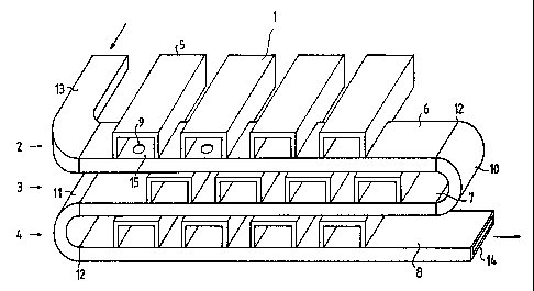
Fig. 1 represents a front view of an array of waveguide
radiators 1, comprising a calibration network according to
a first embodiment of the invention. The waveguide
radiators are arranged to lie in an upper 2, middle 3 and
bottom row 4. The exemplary embodiment comprises only three
rows, but in actual practice there will be dozens of rows
and accordingly, several dozens of waveguide radiators per
row. The waveguide radiators in each row are shifted over a
half a centre-to-centre distance between two waveguide
radiators with respect to the adjacent rows. This yields a
favourable low-sidelobe antenna diagram. This is however
not strictly necessary. At the front side, an iris plate
(not shown) will generally be provided to prevent cross-
talk from one waveguide radiator to another. At the back 5,
the waveguide radiators are generally connected to a
backplane (not shown). The backplane enhances the antenna
rigidity and serves to establish the electrical connection
between the waveguide radiators with their corresponding
T/R (Transmit/Receive) modules. In order to compensate for
phase and amplitude errors which may arise per T/R module
generally as a result of production inaccuracies or
temperature drift, correction factors are determined per
T/R module which are used for the control of the T/R module
in question. To this end, each individual T/R module is at
set times provided with a test signal having a known phase
and amplitude. In order to provide the T/R modules with
such a test signal, a calibration network might for
instance be fitted between the backplane and the T/R
modules. This has several drawbacks, though. Firstly, space
CA 02215744 1997-09-16
R'O 96/30963 PC'T/EP96101146
7
should be created between the T/R modules and the backplane
to accommodate the calibration network. To bridge this gap,
a connecting line has to be mounted between each waveguide
radiator and related T/R module, which entails losses.
Secondly, phase and amplitude errors arising past the
backplane are not included in the correction procedure. In
the exemplary embodiment the calibration network comprises
a number of waveguides 6, 7, 8 which are mounted along the
widest side walls of the waveguide radiators. Each
waveguide radiator comprises a coupling device 9 shaped as
a hole, which is illustrated for one waveguide radiator
only. The coupling device is preferably designed as a prior
art directional coupling, the coupling of energy being
substantially in the direction of the backplane.
Directional couplers can for instance be designed as two
diagonal holes in the rectangle formed by the overlap of
the waveguide and a waveguide radiator. A coupling device
is required only for those waveguide radiators to be
calibrated. This generally obtains for all waveguide
radiators, although it is not strictly necessary.
It is also possible to make several holes per waveguide
radiator. The waveguides 6, 7, 8 are interconnected by
waveguide bends 10, 11, which can be attached by means of
flanges 12. Consequently, one test signal suffices for the
entire system of waveguides. The system of waveguides
curves towards the backplane via a bend 13 which renders
the backplane suitable for providing a test signal. At the
end 14 of the system of waveguides, a matched load (not
shown) is preferably provided to avoid test signal
reflections. It is of course also possible to provide, per
row of radiating elements, each waveguide with a test
signal and a matched load. Bends 10, 11 are then omitted.
In the event of a test signal generator failure, it is
still possible to provide the other rows with a test
signal. In the exemplary embodiment, the waveguide
CA 02215744 1997-09-16
WO 96130963 PCT/EP96/01146
8
radiators consist of rectangular elements, the lower side
walls of which have been removed at the waveguide
interface. The top 15 of the waveguide thus constitutes the
lower side wall. This has the advantage that only the
waveguide has to be provided with one or more holes. -
Fig. 2A and fig. 2B show a magnified view of a waveguide
radiator 1. The waveguide radiator is rectangular in shape.
At the waveguide 6, it has an inverted U-shape, owing to
to the lower side wall having been removed. Behind the
waveguide, the waveguide radiator continues as a
rectangular element, as shown in fig. 2B. This way, the
narrow back sidewall 16 of the waveguide 6 thus abuts on
the raised edge 17 of the waveguide radiators where the
lower side wall 18 of the waveguide radiators starts and
continues in the direction of the backplane. This enables
the waveguide radiators to be correctly positioned during
assembly.
Fig. 3 shows a second embodiment of the phased array
antenna provided with the calibration network according to
the invention. The waveguide radiators 19 are mounted on
both sides of the waveguides. This effects a 50% reduction
of the required length of waveguide 20, 21, 22. The
waveguides 20, 21, 22 are on both sides provided with holes
23 at the waveguide radiators for the coupling of a test
pulse. The waveguide radiators 19 are provided with
corresponding holes 24. In the exemplary embodiment, the
waveguide radiators are rectangular throughout their entire
length. A matched load 25 is mounted at the end of the
waveguide 22. The test pulse is introduced at the input 26
of the waveguide 20.
Fig. 4 shows a method of attaching a rectangular waveguide
radiator 27 to the waveguide 28 of the calibration network
CA 02215744 1997-09-16
WO 96/30963 PCT/EP96/01146
9
that differs from that shown in fig. 1. A section 29 having
the width of a waveguide radiator side wall has been
removed from the upper=side wall 30 of the waveguide 28.
This creates a recess which substantially accurately fits
the rectangular waveguide radiator 27. The waveguide
radiator is provided with a hole 31 to enable the coupling
of radiant energy.
Phased array antennas according to the invention are by no
means restricted to the above-mentioned embodiments.
Features from the above-mentioned embodiments can be
applied in combination.