Note: Descriptions are shown in the official language in which they were submitted.
CA 0221~9~9 1997-09-19
WO 96/29711 PCTtUS96/03469
EI.ECTRIC~L DEVICE
BA~KGROUND OF THE INVEN~ION
Field of the Tnvention
This invention relates to electrical devices compri~ing conductive polymer
compositions and methods for making such devices.
Introduction to the Invention
Electrical devices compri.~ing conductive polymer compositions are well-known.
Such compositions comprise a polymeric component and, dispersed therein, a particulate
conductive filler such as carbon black or metal. Conductive polymer compositions are
described in U.S. Patent Nos. 4,237,441 (van Konynenburg et al), 4,388,607 (Toy et al),
4,534,889 (van Konynenburg et al), 4,545,926 (Fouts et al), 4,560,498 (Horsma et al),
4,591,700 (Sopory), 4,724,417 (Au et al), 4,774,024 (Deep et al), 4,935,156 (vanKonynenburg et al), 5,049,850 (Evans et al), 5,250,228 (Baigrie et al), 5,378,407
(Chandler et al), and 5,451,919 (Chu et al), in U.S. Application No. 08/408,769
(Wartenberg et al, filed March 22, 1995), and in Tntern~tional Application No.
PCT/US95/07925 (Raychem Corporation, filed June 7, 1995). These compositions often
exhibit positive temperature coefficient (PTC) behavior, i.e. they increase in resistivity in
response to an increase in temperature, generally over a relatively small t~l.lpe
range. The size of this increase in resistivity is the PTC anomaly height.
PTC conductive polymer compositions are particularly suitable for use in
electrical devices such as circuit protection devices that respond to changes in ambient
temperature and/or current conditions. Under normal conditions, the circuit protection
device remains in a low temperature, low reSi~t~nce state in series with a load in an
electrical circuit. When exposed to an ov~ l or overtemperature condition,
however, the device increases in resistance, effectively shutting down the current flow to
the load in the circuit. For many applications it is desirable that the device have as low a
re~i~t~nce and as high a PTC anomaly as possible. The low resistance means that there is
little contribution to the resistance of the electrical circuit during normal operation. The
high PTC anomaly allows the device to withstand the applied voltage. Although low
resistance devices can be made by ch~n~ing ~iimen~ions, e.g. making the distancebetween the electrodes very small or the device area very large, the most common
CA 0221~9~9 1997-09-l9
WO 96/29711 PCT/US96/03469
technique is to use a composition that has a low resistivity. The resistivity of a
conductive polymer composition can be decreased by adding more conductive filler, but
this generally reduces the PTC anomaly. A possible explanation for the reduction of the
PTC anomaly is that the addition of more con-1netive filler (a) decreases the amount of
crystalline polymer that contributes to the PTC anomaly, or (b) physically ~ rol~;es the
polymeric component and thus decreases the expansion at the melting temperature. It is,
therefore, often difficult to achieve both low resistivity and high PTC anomaly.
SUMM~RY OF THE INVEN~ION
Even when a low resistivity composition is prepared, the numerous processing
steps required to fabricate a circuit protection device often contribute to an increase in
device resistance. Processes that are used to improve the electrical stability of a device,
e.g. cro~linking of the conductive polymer, or heat-tre~tment, often increase resistance.
One cornmon technique for plC~;llg devices is to punch or cut devices from a sheet of
conductive polymer l~min~tçcl with metal electrodes. While it has been proposed in U.S.
Patent No. 5,303,115 (Nayar et al) that deliberately in(11lce(1 damage at the edges of
specialized thick, highly crosslinked devices can be useful in meeting the requirements of
a severe electrical test such as those set forth in Und~l ~fil~l 's Laboratory Standard 1459
(June 5, 1990 and December 13, 1991), we have now recognized that even routil~e
pnnching processes on relatively thin devices can induce damage, e.g. microscopic cracks
at the perimeter of the device. This damage decreases the PTC anomaly height andadversely affects electrical performance. There is, therefore, a need for a device that,
after pnnching and proce~ing, retains a low resistance and a high PTC anomaly, and
exhibits good electrical stability.
We have now discovered that electrical devices with low resi~t~nce, high PTC
anomaly, good electrical stability and reproducibility can be prepared by following a
particular processing technique. In a first aspect, this invention discloses an electrical
device which comprises
(A) a resistive element which is composed of a conductive polymer
composition which compri~çc
(1) a polymeric component having a crystallinity of at least 20% and a
melting point Tm~ and
CA 0221~9~9 1997-09-19
WO 96129711 PCTIUS96/03469
(2) dispersed in the polymeric component a particulate conductive
filler, and
(B) two electrodes which (i) are ~tt~-.h~l to the resistive element, (ii)
comprise metal foils, and (iii) can be connected to a source of electrical
power,
the device having been prepared by a method which compr1~cs the steps of
(a) cutting the device from a l~min~tç compri~ing the conductive polymer
composition positioned between two metal foils;
(b) exposing the device to a thermal tre~tment at a temperature Tt which is
greater than Tm after the cutting step; and
(c) cro.~linking the conductive polymer composition after the thermal
treatment step,
said device having at least one of the following characteristics:
(i) a resistive elPment thickness of at most 0.51 mm;
(ii) a cro~linking level equivalent to 1 to 20 Mrads;
(iii) the cro.c~linking was accomplished in a single process;
(iv) a resistance at 20~C, R20, of at most 1.0 ohm; and
(v) a resistivity at 20~C, P20, of at most 2.0 ohm-cm.
In a second aspect, the invention discloses an electrical device which compri.~es
(A) a resistive element which (i) has a thickness of at most 0.51 mm, (ii) is
cros.~linkecl to the equivalent of at least 2 Mrads, and (iii) is composed of
a conductive polymer composition which compri~ç~
CA 0221~9~9 1997-09-19
WO 96/29711 PCT/US96/03469
(1) a polymeric component having a crystallinity of at least 20% and a
melting point Tm~ and
(2) dispersed in the polymeric component a particulate conductive
filler; and
(B) two electrodes which (i) are ~tt~-.hPd to the resistive element, (ii)
cnmpri~e metal foils, and (iii) can be connected to a source of electrical
power,
the device
(a) having a resistance at 20~C, R20, of at most 1.0 ohm,
(b) having a resistivity at 20~C, P20, of at most 2.0 ohm-cm,
- (c) having a PTC anomaly, PTC, from 20~C to (Tm + 5~C) of at least 105,
and
(d) having been prepared by a method in which
(1) the device has been cut in a cutting step from a l~min~te
comprising the conductive polymer composition positioned
between two metal foils, and
(2) the device has been exposed to a thermal tre7-trnent at a
temperature Tt which is greater than Tm after the cutting step and
before a cro.c~linking step.
In a third aspect, the invention discloses a method of making an electrical device
which comprises
(A) a resistive element which (i) has a thickness of at most 0.51 mm, (ii) is
crosslinked to the equivalent of at least 2 Mrads, and (iii) is composed of
a conductive polymer composition which comprises
(1) a polymeric component having a crystallinity of at least 20% and a
melting point Tm~ and
CA 0221~9~9 1997-09-l9
WO 96/29711 PCT/US96/03469
(2) dispersed in the polymeric component a particulate conductive
filler; and
(B) two electrodes which (i) are ~tt~-.hed to the resistive element, (ii)
comprise metal foils, and (iii) can be connected to a source of electrical
power,
said method compri~in~
(a) preparing a l~min~t~ compr-~in~ the conductive polymer composition
positioned between two metal foils,
(b) cutting a device from the l~min~tf-,
(c) exposing the device to a thermal trÇ~tment at a te~ .dLulc: Tt which is
greater than Tm~
(d) cooling the device, and
(e) cro.~slinking the device.
:E~RIEF DESCRIPTION OF THE ORAW~G
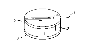
The invention is illustrated by the drawing in which Figure 1 shows a plan view of
an electrical device of the invention;
- Figure 2 shows a plan view of a l~minz~te from which devices of the invention can
be pre~cd;
Figure 3 shows the resistivity as a function of LelllpeldLul~ for devices made by a
conventional method and by the method of the invention; and
Figure 4 shows the resistance as a function of Lelllp~ldLùl~ for devices made by a
35 conventional method and by the method ofthe invention.
CA 022l~9~9 l997-09-l9
WO 96/29711 PCT/U~396/03469
DFTATT Fn DFSCRIPTION OF THF INVFNTION
The electrical device of the invention compri~es a resistive element composed of a
conductive polymer composition. This composition comprises a polymeric componentcnmpri~ing one or more crystalline polymers. The polymeric component has a
crystallinity of at least 20%, preferably at least 30%, particularly at least 40%, as
measured by a dirr~lell~ial sç~nnin,~ calorimeter (DSC). It is plcrelled that the polymeric
component comprise polyethylene, e.g. high density polyethylene, medium density
polyethylene, low density polyethylene, or linear low density polyethylene; an ethylene
10 copolymer or terpolymer, e.g. ethylene/acrylic acid copolymer (EAA), ethylene/ethyl
acrylate (EEA), ethylene/butyl acrylate (EBA), or other copolymer such as those
described in Tntçrn~tional Application No. PCT/US95/07925 (Raychem Corporation,
filed June 7, 1995); a fluoropolymer, e.g. polyvinylidene fluoride (PVDF); or a llli~Lule
of two or more of these polymers. High density polyethylene that has a density of at least
15 0.94 g/cm3, generally 0.95 to 0.97 g/cm3, is particularly plt;relled. For some applications
it may be desirable to blend the crystalline polymer(s) with one or more additional
polymers, e.g. an elastomer or an amorphous thermoplastic polymer, in order to achieve
specific physical or thermal ~lvp~l lies~ e.g. flexibility or m;l x i~ exposure t~ ldLule.
The polymeric component generally compri~ç~ 40 to 80% by volume, preferably 45 to
20 75% by volume, particularly 50 to 70% by volume of the total volume of the
composition. When the composition is intrn~lçrl for use in a circuit protection device that
has a resistivity at 20~C of at most 2.0 ohm-cm, it is plt;r~ d that the polymeric
component comprise at most 70% by volume, preferably at most 66% by volume,
particularly at most 64% by volume, especially at most 62% by volume of the total
25 volume of the composition.
The polymeric component has a melting temperature, as measured by the peak of
the endotherm of a ;lirrel~lllial sr~nning calorimeter, of Tm. When there is more than one
peak, Tm is defined as the tt~ clillule of the highest t~ dlule peak.
Dispersed in the polymeric component is a particulate conductive filler. Suitable
conductive fillers include carbon black, graphite, metal, e.g. nickel, metal oxide,
conductive coated glass or ceramic beads, particulate conductive polymer, or a
combination of these. Such particulate conductive fillers may be in the form of powder,
35 beads, flakes, or fibers. It is pler~;llc:d that the conductive filler comprise carbon black,
and for compositions used in circuit protection devices it is particularly pler~ d that the
carbon black have a DBP number of 60 to 120 cm3/lOOg, preferably 60 to 100 cm3/lOOg,
particularly 60 to 90 cm3/lOOg, especially 65 to 85 cm3/lOOg. The DBP number is an
CA 0221~9~9 1997-09-l9
WO 96/29711 PCT/US96/03469
indication of the amount of structure of the carbon black and is ~letermin~d by the volume
of n-dibutyl phths~l~t~ (DBP) absorbed by a unit mass of carbon black. This test is
described in ASTM D2414-93. The quantity of conductive filler needed is based on the
required resistivity of the composition and the resistivity of the conductive filler itself.
Generally the particulate conductive filler c-~mpri~ec 20 to 60% by volume, preferably 25
to 55% by volume, particularly 30 to 50% by volume of the total composition. If the
composition is int~ntle-l for use in a circuit protection device that has a resistivity at 20~C
of at most 2.0 ohm-cm, the conductive filler preferably comprises at least 30% by
volume, particularly at least 34% by volume, especially at least 36% by volume, most
especially at least 38% by volume of the total volume of the composition.
The conductive polymer composition may comprise additional components
including antioxicl~nt.c, inert fillers, nonconductive fillers, radiation cro~linkin~ agents
(often referred to as prorads or cro~linking enhancers), stabilizers, dispersing agents,
coupling agents, acid scavengers (e.g. CaCO3), or other components. These components
generally comprise at most 20% by volume of the total composition.
The composition exhibits positive temperature coefficient (PTC) behavior, i.e. it
shows a sharp increase in resistivity with temperature over a relatively small telllpcl~ e
range. The term "PTC" is used to mean a composition or device that has an Rl4 value of
at least 2.5 andlor an Rloo value of at least 10, and it is ~l~felled that the composition or
device should have an R30 value of at least 6, where Rl4 is the ratio of the resistivities at
the end and the beginnin~ of a 14~C range, Rloo is the ratio of the resistivities at the end
and the beginning of a 100~C range, and R30 is the ratio of the resistivities at the end and
the beginning of a 30~C range. Compositions used for devices of the invention show a
PTC anomaly over the range from 20~C to (Tm + 5~C) of at least 104, preferably at least
104 5, particularly at least 105, especially at least 1055, i.e. the log[(re~i~t~nre at (Tm +
5~C)/resistance at 20~C] is at least 4.0, preferably at least 4.5, particularly at least 5.0,
especially at least 5.5. If the m~ximllm reCict~n~ e is achieved at a temperature Tx that is
below (Tm + 5~C), the PTC anomaly is ~let~rmin~l by the log(resistance at Tx/resistance
at 20~C). In order to ensure that effects of processing and thermal history are neutralized,
at least one thermal cycle from 20~C to (Tm + 5~C) and back to 20~C should be conducted
before the PTC anomaly is measured.
While dispersion of the conductive filler and other components in the polymeric
component may be achieved by any suitable means of mixing, including solvent-mixing
it is pl~r~led that the composition be melt-processed using melt-processing equipment
including mixers made by such m~nllf~ tllrers as Brabender, Moriyama, and Banbury,
CA 0221~9~9 1997-09-19
WO 96/29711 PCTrUS~6/03169
and continuous compounding equipment, such as co- and counter-rotating twin screw
extruders. Prior to mixing, the components of the composition can be blended in a
blender such as a T-Ten~t~helTM blender to illl~JlOV~ the ullirolllliLy of the mixture loaded
into the mixing eql]ipm~nt The composition can be prepared by using a single melt-
5 mixing step, but it is often advantageous to prepare it by a method in which there are twoor more mixing steps, as described in U.S. Application No. 08/408,769 (Wartenberg et al,
filed March 22,1995). During each mixing step the specific energy consumption (SEC),
i.e. the total amount of work in MJ/kg that is put into the composition during the mixing
process, is recorded. The total SEC for a composition that has been mixed in two or more
10 steps is the total of each of the steps. Depending on the amount of particulate filler and
polymeric component, a composition made by a multiple mixing process suitable for use
in some devices of the invention, i.e. circuit protection devices, has a relatively low
resistivity, i.e. less than 10 ohm-cm, preferably less than 5 ohm-cm, particularly less than
1 ohm-cm, while m~;"~ ;"p~ a suitably high PTC anomaly, i.e. at least 4 clec~de~,
15 preferably at least 4.5 ~cc~des
After mixing, the colll~osilion can be melt-shaped by any suitable method, e.g.
melt-extrusion, injection-molding, colll~l~ssion-molding, and sint~ring, in order to
produce a resistive element. The element may be of any shape, e.g. rectangular, square,
20 circular, or armular. For many applications, it is desirable that the composition be
extruded into sheet from which the resistive element may be cut, diced, or otherwise
removed. In one aspect of the invention, the resistive element has a thickness of at most
0.51 mm (0.020 inch), preferably at most 0.38 mm (0.015 inch), particularly at most 0.25
mm (0.010 inch), especially at most 0.18 mm (0.007 inch).
Electrical devices of the invention may comprise circuit protection devices,
heaters, sensors, or resistors in which the resistive element is in physical and electrical
contact with at least one electrode that is suitable for connecting the element to a source
of eleckical power. The type of electrode is dependent on the shape of the element, and
30 may be, for example, solid or stranded wires, metal foils, metal meshes, or metallic ink
layers. Electrical devices of the invention can have any shape, e.g. planar, axial, or
dogbone, but particularly useful devices comprise two laminar electrodes, preferably
metal foil electrodes, with the conductive polymer resistive element sandwiched between
them. Particularly suitable foil electrodes have at least one surface that is
35 electrodeposited, preferably electrodeposited nickel or copper. Appropriate electrodes are
disclosed in U.S. Patents Nos. 4,689,475 (~A~tthies~n),4,800,253 (K~einer et al), and
Tntern~tional Application No. PCT/us95/07888 (Raychem Corporation, filed June 7,1995). The electrodes may be z~ rht?~l to the resistive element by colll~lession-molding,
CA 0221~9~9 l997-os-ls
WO 96/29711 PCT/US96/03469
nip-l~min~tion, or any other a~.o~!fiate technique. Additional metal leads, e.g. in the
form of wires or straps, can be ~tt~rhe~l to the foil electrodes to allow electrical
connection to a circuit. In addition, elements to control the thermal output of the device,
e.g. one or more cnn~ ctive termin~l~, can be used. These termin~l~ can be in the form of
S metal plates, e.g. steel, copper, or brass, or fins, that are ~tt~rhecl either directly or by
means of an intrrm~ te layer such as solder or a conductive adhesive, to the electrodes.
See, for example, U.S. Patent Nos. 5,089,801 (Chan et al) and 5,436,609 (Chan et al).
For some applications, it is ~,lert;l-ed to attach the devices directly to a circuit board.
Examples of such ~tt~rhment techniques are shown in Tnt.orn~tional Application Nos.
PCT/US93/06480 (Raychem Corporation, filed July 8, 1993), PCT/US94/10137
(Raychem Corporation, filed September 13, 1994), and PCT/US95/05567 (Raychem
Corporation, filed May 4, 1995). ~
In order to improve the electrical stability of the device, it is generally n. cee~z3ry
15 to subject the resistive element to various processing techniques, e.g. cro.~linking and/or
heat-tre~tment, following shaping, before and/or after ~tt~rhment of the electrodes.
Cro~elinkinp can be accomplished by chemical means or by irradiation, e.g. using an
electron beam or a Co60 ~ irradiation source. The level of croc~linkinF depends on the
required application for the composition, but is generally less than the equivalent of 200
20 Mrads, and is preferably subst~nti~lly less, i.e. from 1 to 20 Mrads, preferably from 1 to
15 Mrads, particularly from 2 to 10 Mrads for low voltage (i.e. less than 60 volts)
applications. Useful circuit protection devices for applications of less than 30 volts can
be made by irr~ tin~ the device to at least 2 Mrads but at most 10 Mrads.
We have found that subst~nti~lly improved electrical stability and PTC anomaly
can be achieved if, after the device is cut from a l~min~t~ comprising the conductive
polymer composition positioned between two metal foils, the device is exposed to a
thermal tre~tment before cro~linking of the conductive polymer composition is done.
The device is first cut from the l~min~te in a cutting step. In this application, the term
"cutting" is used to include any method of isolating or S~d~d~ g the resistive element of
the device from the l~min~te7 e.g. dicing, plmching, ~h~ring, cutting, etching and/or
breaking as described in Tntern~tional Application No. PCT/US95/07420 (Raychem
Corporation, filed June 8, 1995).
The thermal tre~tment requires that the device be subjected to a temperature Tt
that is greater than Tm~ preferably at least (Tm + 20~C), particularly at least (Tm + 50~C),
especially at least (Tm + 70~C). The duration of the thermal exposure may be very short,
but is sufficient so that the entire conductive polymer in the resistive element reaches a
CA 0221~9~9 1997-09-19
WO 96/29711 PCT/U~;96/03469
~lllpeldLulc of at least (Tm + 5~C). The thermal exposure at Tt is at least 0.5 seconds,
preferably at least 1.0 second, particularly at least 1.5 seconds, especially at least 2.0
seconds. We have found that a suitable thermal tre~tment for devices made from high
density polyethylene or ethylene/butyl acrylate copolymer may be achieved by dipping
S the device into a solder bath heated to a temperature of about 240 to 245~C, i.e. at least
100~C above Tm~ for a period of 1.5 to 2.5 seconds. ~lt~?rn~tively, good results have been
achieved by passing the devices through an oven on a belt and exposing them to atemperature at least 100~C above Tm for 3 seconds. During either one of these ;processes,
electrical leads can be ~tt~ch~l to the electrodes by means of solder.
After exposure to the therrnal tre~tnnent, the device is cooled to a te~ ,.dLu~
below Tm~ i.e. to a ten~eldLule of at most (Tm - 30~C), preferably at most (Tm - 50~C),
especially at most (Tm - 70~C). It is particularly ~lcfc.led that the device be cooled to a
telll~ dLule at which the conductive polymer composition has achieved 90% of it
15 m~x;".ll", cryst~lli7~tion. Cooling to room temperature, particularly to 20~C, is
particularly preferred. The cooled device is then crosclinke~l preferably by irradiation.
Devices of the invention are preferably circuit protection devices that generally
have a recict~n~e at 20~C, R20, of less than 100 ohms, preferably less than 20 ohms,
20 particularly less than 10 ohrns, especially less than 5 ohms, most especially less than 1
ohm. It is particularly preferred that the device have a recict~n~e of at most 1.0 ohm,
preferably at most 0.50 ohm, especially at most 0.10 ohm, e.g. 0.001 to 0.100 ohm. The
resistance is measured after one thermal cycle from 20~C to (Tm + 5~C) to 20~C. Heaters
generally have a resistance of at least 100 ohms, preferably at least 250 ohms, particularly
25 at least 500 ohms.
When in the form of a circuit protection device, the device has a resistivity at20~C, P20, of at most 10 ohm-cm, preferably at most 2.0 ohm-cm, particularly at most 1.5
ohm-cm, more particularly at most 1.0 ohm-cm, especially at most 0.9 ohm-cm, most
30 especially at most 0.8 ohm-cm. When the electrical device is a heater, the resistivity of
the conductive polymer composition is generally snhst~ntizllly higher than for circuit
protection devices, e.g. 1 o2 to 10~ ohm-cm, preferably 1 o2 to 104 ohm-cm.
Devices made by the method of the invention show hll~lovelllent in PTC anomaly
35 over devices prepared by conventional methods in which the l~min~te is crocclinke~l
before the device is cut. Thus a standard device is one made from the same composition
as a device of the invention and following the sdme procedure, except that, for the
standard device, the l~min~te was cro,cclinke~1 before the cutting step. The resistivity P20
CA 0221~9~9 l997-os-ls
Wo 96/29711 PCT/US96/03469
11 .
for a device ofthe invention is less than 1.20p2oC, preferably less than 1.15p2oC, especially
less than l . l 0P2oc~ wherein P20c is the resistivity at 20~C for a standard device measured
following one thermal cycle from 20~C to (Tm + 5~C) to 20~C. In addition, the PTC
anomaly for a device of the invention is at least 1.15PTCC, preferably at least 1 .20PTCC,
particularly at least 1.25PTCC, especially at least 1.30PTCC, wherein PTCC is the PTC
anomaly from 20~C to (Tm + 5~C) for a standard device measured following one thermal
cycle from 20~C to (Tm + 5~C) to 20~C. Often devices of the invention have more than a
40% increase in PTC anomaly height with a relatively small, i.e. less than 20%, increase
in resistivity at 20~C. The difference in resistivity for P20, AP2o~ is ~l~termined from the
formula [(P20 for a device of the invention - P20 for a standard device)/(p20 for a device of
the invention)]. The improvement for the PTC anomaly, ~PTC, is ~l~terminecl from the
formula [(PTC for a device of the invention - PTC for a standard device)/(PTC for a
device of the invention)].
Devices of the invention also show improvement in performance in electrical tests
such as cycle life, i.e. the stability of the device over time when subjected to a series of
electrical tests that convert the device into a high resistance, high te~ cldlule state, and
trip endurance, i.e. the stability of the device over time when powered into a high
resistance, high tclll~ldLule state.
The invention is illustrated by the drawing in which Figure 1 shows an electrical
device 1 of the invention. Resistive element 3, composed of a conductive polymercomposition, is sandwiched between two metal foil electrodes 5,7.
Figure 2 shows l~min~te 9 in which conductive polymer composition 3 is
l~min~t(?cl to first and second metal foil electrodes 5,7. Individual electrical devices 1 can
be cut or punched from l~min~te 9 along the dotted lines.
The invention is illustrated by the following examples, in which Example 1 and
those devices prepared by Processes A, C, E, and G are coll~pa dlive examples.
Ex~m,I~le 1 (Co~ e)
Sixty percent by volume of powdered high density polyethylene (PetrotheneTM
LB832 which has a melting point of about 135~C, available from USI; HDPE) was
preblended in a HenschelTM blender with 40% by volume carbon black beads (RavenTM
430 with a particle size of 82 nm, a structure (DBP! of 80 cm3/100 g, and a surface area
of 34 m2/g. available from Columbian Chemicals; CB), and the blend was then mixed for
CA 0221~9~9 1997-09-19
WO 96/29711 PCI/US96/03469
12
4 min~lte~ in a 3.0 liter MoriyamaTM mixer at 185~C. The ~ Lulc was cooled,
gr~n~ t~-l, and remixed three times for a total mix time of 16 ...i .... I Pc The .. i~Lu.~ was
then co...~.ession-molded to give a sheet with a thickness of 0.18 mm (0.007 inch). The
sheet was l~min~t~d between two layers of electrodeposited nickel foil having a thickness
S of about 0.033 mm (0.0013 inch) (available from Fukuda) by using a press set at 200~C.
The l~min~te was irradiated to 10 Mrads using a 3.0 MeV electron beam, and chips with a
m~tl~r of 12.7 mm (O.S inch) were punched from the lz~min~te Devices were formedfrom each chip by soldering 20 AWG tin-coated copper leads to each metal foil bydipping the chips into a solder form~ tion of 63% lead/37% tin heated to 245~C for
about 2.0 to 3.0 seconds, and allowing the devices to air cool. To ~içtermine the
difference in the PTC anomaly height between the center of the device and the edge, a
ferTic chloride etch was used to remove the metal foil either from the center 6.25 mm
(0.25 inch)-~ metçr section or from the outer 3.175 mm (0.125 inch) perimeter. The
resistance versus temperature properties of the devices were ~letermin~l by posilioning
the devices in an oven and me~llring the resistance at intervals over the temperature
range 20 to 160 to 20~C. Two temperature cycles were run. The height ofthe PTC
anomaly was clçterminecl as log(r.?si~t~n~e at 140~C/re~i~t~nce at 20~C) for the second
cycle, and was recorded as PTC2. The results are shown in Table I.
Example 2
Devices were prepared according to the procedure of Example 1 except that chips
were punched from the l~min~te and leads were ~tt~c he~l by solder dipping prior to
irr~ ting the devices to 10 Mrads. Results, as shown in Table I, indicate that devices
that were soldered before irradiation, and that were exposed to a t~ ldLule during
soldering that was higher than the melting telllpeldLu-~ of the polymer, had higher PTC
anomalies at both the center and edge regions.
Ex~mple 3
Devices were prepared following the procedure of Example 2 except that prior to
etching, the devices were punched again to give a diameter of 8.9 mm (0.35 inch).
Etching was then done for either the 6.25 mm (0.25 inch) center or the outer 1.27 mm
(0.05 inch) perimeter. The results, shown in Table I, indicate that thermal tr~?~tment gave
good PTC anomaly height in the center, but that the subsequent pllnching produced edge
damage that decreased the PTC anomaly height.
CA 0221~9~9 1997-09-19
WO 96129711 = PCT/US96/03469
13
TABLE I
PTC2 Center PTC2 F~e
Fx~m,rle Process (decades) (clçc~d~s)
Trr~ t~/Punch/Solder 5.0 4.7
2 Punch/Solder/lrradiate 6.0 6.0
3 Punch/solder/Trr~ te/punch 6.3 3.4
Fxamples 4 ~n(1 5
Sixty percent by volume of Petrothene LB832 was preblended with 40% by
volume Raven 430, and the blend was then mixed for 16 minlltes in a 60 cm3
BrabenderTM mixer. The mixture was gr~n~ te~l and the granules were then
cc,~ ession-molded to give a sheet with the thickness specified in Table II. Using a
press, the extrudate was l~min~ted between two layers of electrodeposited nickel foil as in
Fx~mrle 1. Devices were then prepared using either the conventional process (Process
A) or the process of the invention (Process B). Following the procedure described for
Example 1, the PTC anomaly height was clçt~rmin~l, and the resistivity at 20~C, P20, was
calculated. The results, shown in Table II, indicate that the PTC anomaly using Process
B was substantially higher than that for Process A. In addition, the difference between
the P20 value and the PTC anomaly for devices prepared by Process A and Process B was
determine-l The difference for P20, ~ P20, was det~rminPd from the formula [(P20 for
Process B - P20 for Process A)/( P20 for Process B)]. The difference for the PTC anomaly,
~ PTC, was fl~termined from the formula [(PTC for Process B - PTC for Process
A)/(PTC for Process B)].
Process A (Conventio~
The l~min~te was irradiated to 10 Mrads using a 3.0 MeV electron beam, and
chips with a diameter of 12.7 mm (0.5 inch) were punched from the l~min~te Devices
were formed from each chip by soldering 20 AWG tin-coated copper leads to each metal
foil by dipping the chips into a solder formulation of 63% lead/37% tin heated to 245~C
for about 3.0 seconds, and allowing the devices to air cool.
CA 022l~9~9 l997-09-l9
WO 96/29711 PCT/US96/03469
14
Process B
Chips with a ~ metrr of 12.7 mm (0.5 inch) were punched from the l~ and
leads were ~t1~rhrd to form a device by soldering 20 AWG tin-coated copper leads to
S each metal foil. Soldering was con~ cted by dipping the chips into a solder f~rmnl~tion
of 63% lead/37% tin heated to 245~C for about 3.0 seconds, and allowing the devices to
air cool. The devices were then irr~ te~l to 10 Mrads using a 3.0 MeV electron beam.
F.~amples 6 to 9
T ~min~tes of different thickn~sscs were prepared following the process of
Example 1. Devices were prepared according to Process A or B. Figure 3 shows theresistivity versus t~ p~,ldlule curve for devices of Example 6 prepared by the
collvelllional Process A, and by Process B, the process of the invention.
Fxam,I~les 10 to 1 2
Sixty-five percent by volume of Petrothene LB832 was preblended with 35% by
volume LampblackTM 101 (carbon black with a particle size of 95 mn, a DBP of 100cm3/l 00 g, a surface area of 20 m2/g, available from Degussa) and the blend was then
mixed for 16 minntes in a Moriyama mixer. The composition was extruded and devices
were prepared according to Process A or B.
Exa~mples 13 to 15
The composition of Examples 10 to 12 was prepared by mixing in a 70 mm (2.75
inch) BussTM kneader. The composition was compression-molded and devices were
prepared according to Process A or B.
CA 0221~9~9 1997-09-l9
WO 96/29711 PCT/US96/03469
TABLE II
Process A Proc ss P~
Thickness Q~Q PTC Q~Q PTC ~Q A PTC
F~mrle 1~ (Q-cm)(decades) (Q-cm!(d~c~{lçs)
4 0.33 1.17 6.9 1.46 9.5 19.9 27.4
0.66 0.75 5.7 0.83 7.4 9.6 23.0
6 0.17 1.33 4.1 1.43 6.8 7.0 39.7
7 0.33 1.30 7.1 1.40 8.5 7.1 16.5
8 0.53 1.50 9.0 1.53 8.9 2.0 -1.1
9 0.91 1.54 8.3 1.66 8.5 7.2 2.4
0.18 0.75 3.6 0.71 6.5 -5.6 44.6
11 0.25 0.76 4.1 0.75 8.6 -1.3 52.3
12 0.51 0.75 5.4 0.83 9.8 9.6 44.9
13 0.14 0.70 3.1 0.80 5.7 12.5 45.6
14 0.30 0.66 4.5 0.75 7.1 12.0 36.6
0.53 0.64 4.4 0.76 5.9 15.8 25.4
Examples 16 to 22
s
The effect of exposing devices CO~ i"i,~f~ dirr~ ll amounts of carbon black to athermal treatment was cletermin~cl by preblending powdered Petrothene LB832 (HDPE)
in a Henschel blender with Raven 430 in the amounts shown by volume percent in Table
III. The blend was then mixed using a 70 mm (2.75 inch) Buss kn~Açr to form pellets.
For Example 21, the pellets of Example 20 were passed through the Buss kn~ r a
second time. For Example 22, the pellets of Example 21 were passed through the Buss
knP~Aer a third time. The total amount of work used during the compounding process,
i.e. the specific energy consumption (SEC) in MJ/kg, was recorded. The pellets for each
composition were extruded through a sheet die to give a sheet with a thickness of 0.25
mm (0.010 inch). The extruded sheet was lz~minzltf d as in F~c~mple 1. Devices were then
prepared by either Process C (a conventional process) or D (a process of the invention).
Process C (Conventional)
The l~min~te was irradiated to 5 Mrads using a 3.0 MeV electron beam, and chips
with a diameter of 12.7 mm (0.5 inch) were punched from the lslmin~te Devices were
CA 0221~9~9 1997-09-19
WO 96129711 PCT/US96/03469
16
formed from each chip by soldering 20 AWG tin-coated copper leads to each metal foil
by dipping the chips into a solder formulation of 63% lead/37% tin heated to 245~C for
about 1.5 seconds, and allowing the devices to air cool.
5 Process D
Chips with a diameter of 12.7 mm (0.5 inch) were punched from the l~min~te and
leads were ~1t~rh~Cl to form a device by soldering 20 AWG tin-coated copper leads to
each metal foil. Soldering was con~ cte~l by dipping the chips into a solder fnrrn~ ti~n
of 63% lead/37% tin heated to 245~C for about 1.5 seconds, and allowing the devices to
air cool. The devices were then irradiated to 5 Mrads using a 3.0 MeV electron beam.
The resistance versus temperature ~lup~;llies ofthe devices were 11t?te~ninPd byfollowing the procedure of Example 1. Resistivity values were calculated from the
15 recorded r~ f~n~e at 20~C on the first and second cycles, Pl and P2, respectively. The
height ofthe PTC anomaly was clet~rrnin~l as log(resistance at 140~C/resistance at 20~C)
for the first and second cycles, and was recorded in ~lec~cles as PTCI and PTC2,respectively. Also calculated were the difference between the resistivity value and the
PTC anomaly for devices prepared by Process C and Process D for both the first and
20 second cycles. The difference for the resistivity at 20~C for the first cycle, ~ Pl, was
~eterrnine~l from the formula [(Pl for Process D - Pl for Process C)/(pl for Process D)].
The difference for the resistivity at 20~C for the second cycle, ~ P2, was ~letP~ninecl from
the formula [(P2 for Process D - P2 for Process C)/(pl for Process D)]. The difference for
the PTC anomaly for the first cycle, ~ PTCI, was ~let~-rrnined from the formula [(PTCI for
25 Process D - PTCI for Process C)/(PTCl for Process D)]. The difference for the PTC
anomaly for the second cycle, ~ PTC2, was determined from the formula [(PTC2 forProcess D - PTC2 for Process C)/(PTC2 for Process D)]. The results, shown in Table III,
indicate that the PTC anomaly for each composition for both the first and second thertnal
cycles was greater for the devices prepared by the process of the invention, i.e. Process D,
30 than that for devices prepared by the conventional process, i.e. Process C. The difference
was particularly marked for the second thertnal cycle. For the second thermal cycle,
although the resistivity was higher for the devices prepared by Process D, the resistivity
increase was subst~nti~lly less than the increase in PTC anomaly.
CA 0221~9~9 1997-09-19
WO 96/29711 PCT/US96/03469
17
TABLE III
F~am,rle 16 17 18 19 20 21 22
CB (Vol%) 32 34 36 38 40 40 40
HDPE (Vol%) 68 66 64 62 60 60 60
SEC (MJ/kg) 2.52 2.48 3.06 3.31 3.64 6.01 8.96
Process C
Pl (ohm-cm) 2.02 1.27 0.98 0.76 0.58 0.65 0.76
PTCI (dec~des) 7.30 6.36 5.81 5.04 3.95 4.89 5.25
P2 (ohm-cm) 2.08 1.34 1.02 0.81 0.56 0.67 0.73
PTC2 (tlec~des) 7.89 6.69 6.19 5.25 4.08 5.09 5.49
Process D
Pl (ohm-cm) 1.48 1.05 0.83 0.70 0.53 0.63 0.65
PTCI (deç~de~)8.397.86 7.38 6.27 4.54 5.79 6.50
P2 (ohm-cm) 2.27 1.47 1.09 0.86 0.60 0.71 0.76
PTC2 (dec~(1es) 8.86 8.29 7.65 6.39 4.58 5.95 6.74
Pl (%) -36.4 -21.0 -18.1 -8.6 -9.4 -3.2 -16.9
~PTCl (%) 13.0 19.1 21.2 19.6 13.0 15.5 19.2
P2 (%) 8.4 8.8 6.4 5.8 6.7 5.6 3.9
~ PTC2 (%) 10.9 19.3 19.1 17.8 10.9 14.5 18.5
Fx~mples 23 to 26
Following the procedure of Example 21, 61 % by volume Petrothene LB832 was
mixed with 39% by volume of Raven 430. The composition was extruded to give a sheet
0.30 mm (0.012 inch) thick, that was nip-lzlmin~ted with two layers of electrodeposited
nickel-copper foil (Type 31. having a thickness of 0.043 mm (0.0013 inch), available
10 from Fukuda) to produce a 1~min~te Devices were then prepared by either Process E (a
conventional process) or F (a process of the invention).
- - -
CA 0221~9~9 1997-09-19
WO 96/29711 PCT/U~96/0346918
Process F (Conventional)
The l~min~te was irr~ t~-1 to 10 Mrads using a 3.0 MeV electron beam, and
chips with ~1imen~inns of 5.1 x 5.1 mm (0.2 x 0.2 inch) or 20 x 20 mm (0.8 x 0.8 inch)
5 were sheared from the l~min~te Devices were formed from each chip by soldering 20
AWG tin-coated copper leads to each metal foil by dipping the chips into a solder
formulation of 63% lead/37% tin heated to 245~C for about 2.5 seconds, and allowing the
devices to air cool. The devices were encapsulated by dipping them into HysolTM DK18-
05 powdered epoxy, an epoxy resin-anhydride compound available from The Dexter
Corporation co.. l~ .g 30 to 60% by weight fused silica, 2% antimony trioxide, 5 to 10%
benzophenonetetracarboxylic dianhydride (BTDA), and 30 to 60% bis-A epoxy resin.The powder was cured at 155~C for 2 hours. The devices were then thenn~lly cycled six
times, each cycle being from -40 to 85 to -40~C at a rate of 5~C/minute with a 30 minute
dwell at-40~C and 85~C.
Process F
Chips with dimensions of 5.1 x 5.1 mm (0.2 x 0.2 inch) or 20 x 20 mm (0.8 x 0.8
inch) were sheared from the l~min~te The chips were then heat-treated using a thermal
profile in which the temperature increased from 20~C to 240~C in 11 seconds, remained
at 240~C for 3 seconds, and then decreased to 20~C over 65 seconds. The chips were
then irradiated, lead-~tt~he-l encapsulated, and therm~lly cycled as in Process E.
The resistance versus tenl~.~;ldLul~ ~lopel lies were ~letermined over the range of 20
to 140~C for two cycles. The PTC anomaly was rletermined as log(resistance at
140~C/reci~t~nre at 20~C) for both cycles and recorded as PTCI for the first cycle and
PTC2 for the second cycle. The results, shown in Table IV, indicate that the devices
made by the conventional process had substantially less PTC anomaly than those made
by the process of the invention. The electrical stability was det~?nnined by testing for
cycle life and trip endurance, described below. The results indicated that, in general, the
devices made by the process of the invention had improved resistance stability.
Cycle Life
Devices were tested in a circuit conci~ting of the device in series with a switch, a
DC power supply of 16 volts, 24 volts, or 30 volts, and a fixed resistor that limited the
initial current to l OOA. Each cycle consisted of applying power to the circuit for 6
seconds to trip the device into the high resistance state, and then turning the power off for
CA 02215959 l997-os-ls
Wo 96129711 PCT/USs6/03469
19
120 secon~1e At intervals, the voltage was removed, the devices were cooled for one
hour, and the r~eiet~nce at 20~C was measured. The n~lrrn~li7~t1 resi.et~nre, RN~ i.e. (the
reeiet~nre at 20~C measured at each interval/the initial reeiet~n~e at 20~C), was reported.
S Trip Fn~1nr~nce
Devices were tested in a circuit coneietin~ of the device in series with a switch, a
DC power supply of either 16 volts or 30 volts, and a fixed resistor that limited the initial
current to 40A. The device was tripped into the high re~eiet~nce state and removed
10 periodically. After each interval, the device was allowed to cool for one hour and the
reeiet~nre at 20~C was measured. The norm~li7rcl rrei.etz~nce, RN~ was reported.
CA 0221~9~9 1997-09-19
WO 96/29711 PCT/US96103469
TABLE IV
Fx~nnple ~ 24 ~ ~
Size(mm) 5.1 x5.1 5.1 x5.1 20x20 20x20
Process E F E F
~e~i~t~nce (mohrns) 70.9 82.1 4.41 4.77
PTCl (decades) 5.0 7.2 5.1 7.2
PTC2 (decades) 4.9 7.5 5.1 7.4
Cycle Life RN
16V: 100 cycles 1.07 1.00 1.10 1.02
500 cycles 3.04 1.30 1.11 1.00
1000 cycles 3.31 2.00 1.16 1.00
2000 cycles 5.34 3.84 1.28 1.04
24V: 100 cycles 1.15 1.32 1.05 1.00
500cycles 1.57 1.56 1.07 0.96
1000 cycles 2.20 2.12 1.11 1.04
2000 cycles 3.59 4.18 1.20 1.10
30V: 100 cycles 1.44 1.22 1.09 1.04
500 cycles 1.63 1.10 1.01
1000 cycles 1.81 1.17 1.07
2000 cycles 3.10 1.25 1.11
Trip endurance RN
16V: 5 ~ 1.23 1.22 1.26 1.15
24 hours 1.35 1.21 1.35 1.16
96 hours 1.68 1.45 1.53 1.25
366 hours 2.78 2.31 2.00 1.57
723 hours 4.23 3.39 2.71 1.89
30V: 5 lllillUL~1.3~ 1.26 1.34 1.16
24 hours 2.04 1.32 1.60 1.24
96 hours 2.59 1.82 1.71
366 hours 10.6 3.54 2.23 1.63
723 hours 595 7.56 2.93 1.98
CA 0221~9~9 1997-09-19
WO 96/29711 PCT/US96/03469
21
F.x~mples 27 ~n~1 28
Sixty-four percent by volume of ethylene/n-butyl acrylate copolymer (Fn~theneTM
EA 705-009, c~ g 5% n-butyl acrylate, having a melt index of 3.0 g/10 min, a5 melting temperature of 105~C, available from Q~.LI~11. Cht~n~ Corporation) waspreblended with 36% by volume Raven 430, and the blend was then mixed for 12
.e in a 350 cm3 Br~benrler mixer heated to 175~C. The llli~ c was gr~n~ te~1 thegranules were extruded into a sheet, and the sheet was l~min~tecl in a press between two
layers of Type 31 foil. Devices of Example 27 were prepared by Process G (a
10 conventional process), devices of Example 28 were prepared by Process ~I (a process of
the invention).
Process G (Conventional)
The l~ e was irradiated to 10 Mrads using a 3.0 MeV electron beam and
chips with tlimenejons of 5.1 x 12.1 x 0.23 mm (0.2 x 0.475 x 0.009 inch) were cut from
t_e l~min~te Devices were formed by soldering 20 AWG leads as in Process E. Device
reeiet~nee at 20~C was 0.071 ohms.
20 ProcessH
Chips with t1imeneions of 5.1 x 12.1 x 0.23 mm (0.2 x 0.475 x 0.009 inch) were
cut from the l~min~te Leads were ~ttsll~hecl as in Process E and the devices were then
heat-treated by exposure to 290~C in a reflow oven for about 3.5 seconds. After cooling
25 to room tenl~ldLul~, the devices were irradiated to 10 Mrads using a 3 MeV electron
beam. Device reeiet~nce at 20~C was 0.096 ohms.
Figure 4 shows a curve of the resistance in ohms as a function of L~ )eldLUle for
Examples 27 and 28. It is d~ llL that a device made by the process of the invention has
30 substantially higher PTC anomaly than a device made by a conventional processes.