Note: Descriptions are shown in the official language in which they were submitted.
CA 02216037 1997-09-17
JC:tdy 8/29/97 247-44577.app ~ 1 ~
PORTABLE MICROWAVE MOISTURE MEASUREMENT
INSTRUMENT USING TWO MICROWAVE SIGNALS OF
DIFFERENT FRE~u~Y AND PHASE SHIFT DET~MTN~TION
BACKGROUND OF THE lNV~!;NLlON
The present invention relates to the measurement
of unknown properties of materials, such as moisture
content or dielectric constant, using microwaves and in
particular to a portable microwave instrument for the
measurement of the moisture content of a material by
transmitting microwave beams through such material so
that a portion of the beam energy is absorbed by the
moisture or other property. This percent moisture
measurement is achieved with good accuracy in spite of
the presence in the test material of another microwave
absorbing property or component in variable amounts, by
measuring attenuation using two beams of two microwave
signals of different frequency and determining the
density of the test material by measuring the phase
shift of the received signal produced by one of such
signals when its corresponding microwave beam is
transmitted through the test material. The invention
also includes a microwave antenna with two microwave
signal connections for the two different frequency
signals properly positioned in order to efficiently
transmit or receive two microwave beams of different
frequency with the same antenna without interference.
In addition, the present invention includes a
temperature compensation circuit employing two
thermistors, for each of two PIN diode attenuators that
attenuate the received microwave signals in response to
control signals in order to adjust the attenuation
characteristics of the attenuators in compensation for
changes in temperature. A second temperature
compensation circuit including one thermistor is
employed for maintaining the frequency of the microwave
signal source used for phase measurement substantially
constant by making compensating changes in the source
supply voltage. Microwave signal connectors are
CA 022l6037 l997-09-l7
JC:tdy 8/29/97 247-44577.app ~ 2
employed in the portable microwave moisture measurement
instrument to separate the outer conductors of
interconnected microwave signal waveguides, such as
coaxial cable connectors, to eliminate DC voltage
coupling and to strongly attenuate low frequency
modulation signals of 10 to 20 kHz but to allow low
impedance AC voltage coupling at microwave frequencies
with low attenuation. Also the test material is held in
test containers of different sizes and an electrical
sensor is provided to sense the size of the selected
container using different patterns of conductive strips
on each container and to produce a sensor output signal
corresponding to the selected container size.
The present invention is especially useful in
measuring the moisture content of various materials. In
the previous U.S. Patent Nos. 3,696,894, 3,818,333,
4,475, 080 and 4,727,311 of Charles W.E. Walker issued
September 19, 1972, June 18, 1974, October 2, 1984 and
February 23, 1988, respectively, and in the paper
" Instrumentation For The On Stream Analysis Of Ash
Content And Moisture Content In Coal Cleaning Plants" by
Gunter Fauth, et al., published at the annual meeting of
S.M.E. and A.I.M.E. at Los Angeles, California
February 26 to March 1, 1984, microwave moisture
measurement apparatus is disclosed. However, these
prior apparatus do not disclose a portable instrument
using two microwave beams of different frequency to
determine the amount of moisture attenuation of the
microwave beams by the test material, by attenuation of
the received microwave signals using temperature
compensated PIN diode attenuators with thermistors to
adjust the attenuation characteristics and to measure
the phase shift of one of the two attenuated received
microwave signals to determine test material density for
measurement of the percent of moisture content, in the
manner of the present invention. In addition, they do
not show a portable microwave moisture measurement
instrument having microwave isolation connectors to
CA 02216037 1997-09-17
JC:tdy 8/29/97 247-44577.app - 3
isolate the outer conductors of interconnected
waveguides from DC voltage coupling but allowing low
impedance AC coupling at microwave frequencies.
Furthermore, such prior patents do not disclose a
portable microwave moisture measurement instrument in
which the test material is held in test containers of
different sizes and an electrical sensor is provided to
sense the size of the selected container and produce a
sensor output signal corresponding to the selected
container size.
The invention is directed to the accurate
measurement of the moisture content of a wide range of
solid and liquid materials. Also the portable
instrument can be used to measure electrical
conductivity including the conductivity of ground water
in pollution control equipment. In the above noted
patents, it is shown that the absorption of microwave
energy from a microwave beam transmitted through the
material is capable of providing accurate information on
its moisture content. The present inventor has found,
however, that in all materials there are interfering
effects or other factors present in the material, in
addition to the amount of water present, which affect
the microwave absorption.
All substances in the dry state produce some
microwave absorption. In some, this microwave
absorption is constant but in many of the materials
which are industrially important, it is not constant and
must be measured by an independent means if accurate
measurement of moisture is to be obtained. In some
cases, for example, the dry attenuation of the microwave
is due to the dry substance being electrically
conductive. If this is true in the macroscopic sense,
the substance is probably not ~m~n~hle to measurement by
microwaves but many substances such as foundry molding
sand and most coals are not electrically conducting in
the macroscopic sense, yet contain microscopic particles
or aggregates of atoms which are conductive and which,
CA 02216037 1997-09-17
JC:tdy 8/29/97 247-44577.app ~ 4
as a result, attenuate a microwave signal passed through
the substance. In the case of both coal and foundry
sand, this observed dry attenuation is thought to be due
to elemental carbon particles, possibly in the form of
small graphite crystallites. Finely divided metallic
particles could have the same effect. Whatever the
cause, the microwave attenuation due to such electrical
conductivity is not frequency dependent, and so is
markedly different from the water resonant absorption.
The same is true of ionic conductivity which is another
form of electrical conductivity and may arise from the
presence of salts or of acids or bases in the substance
being measured since any of these will dissolve in any
7ater which is present to produce ions. Ionic
conductivity will not contribute to dry attenuation but
will affect the microwave attenuation so as to add to
the moisture sensitivity in proportion to the ionic
concentration. If this electrical conductivity of the
dry material is not constant or the ionic concentration
varies, then an independent measurement is needed to
account for it if accurate moisture measurement is to be
obtained.
In microwave moisture measurement, the
microwaves are passed through the test material and
therefore sense a certain volume of material and are
absorbed in proportion to the number of water molecules
in that sense volume. The measurement signal is
therefore proportional to the mass of water per unit
volume in the material. To express this as percent
water requires that the mass of material in the volume
sensed be known. This may require a measurement of the
thickness or volume of material through which the
microwaves are passed and the density of the material in
that volume.
Yet another factor which affects the microwave
moisture measurement readings is that some of the water
present becomes bonded to the material. This may be
physical, as for example Van Der Waals' forces. In
CA 02216037 1997-09-17
JC:tdy 8/29/97 247-44577.app ~ 5
either case, the water molecules so bonded are not free
to rotate as free molecules and so do not exhibit the
resonant interaction with microwaves. Except for
hydrogen bonding of water to cellulose and starch
molecules which produce a square law relationship
between microwave attenuation and percent water, the
present inventor found that almost all substances
exhibit an interaction which appears to be a surface
bonding phenomenon because it is dependent on particle
size and particularly on the finest particles present.
Thus, in pure silica sand there is effectively no
bonding to a coarse grade but over 1~ water bonds to 32
mesh grade sand. The net effect of the bonding in most
substances, other than the organic ones mentioned above,
is to halve the microwave attenuation up to the
saturation level at which all the available bonds are
satisfied. Beyond this point the attenuation becomes
normal. For accurate moisture measurement through this
saturation level, it is necessary that this level be
known and that it be measured if it is not constant.
This generally requires a knowledge of the fines
content. Thus, in foundry molding sand it is the finely
powdered Bentonite clay which establishes this level.
To eliminate these disturbing factors and for
accurate moisture measurement, it is essential therefore
that at least three independent measurements be made.
Only in special cases, can some of these be replaced
with constant subtractors or divisors or by periodic
manual adjustments as, for example when lower accuracy
is acceptable, or when measuring some substances such as
ammonium phosphate fertilizer in which the ionic
conductivity is directly proportional to the amount of
water present and so may be accounted for by a constant
calibrating factor. In some other cases where moisture
determination is only required over a limited range of
moisture which is known to be either wholly below or
wholly above the level at which bonding is saturated, it
may not be necessary to measure this level.
CA 02216037 1997-09-17
- JC:tdy 8/29/97 247-44577.app ~ 6
It is therefore the specific purpose of this
invention to provide the additional independent
measurement means, in addition to the simple microwave
attenuation, which are needed as stated above to provide
accurate moisture measurement.
The present inventor has determined that the
effect of dry attenuation due to electrical conductivity
can be eliminated by making microwave attenuation
- measurements at two different microwave frequencies.
Because this dry attenuation is not frequency sensitive,
the difference between the attenuation signals at the
two different microwave frequencies is independent of
such dry attenuation and depends only on the water
present. This dual frequency measurement also
eliminates the effect of variations in ionic
conductivity when this is a concern. It is perhaps
worth noting that there are some special cases such as
alcohol and heavy water in which dry attenuation is
frequency sensit-ive because these substances have their
own resonant interaction with microwaves within the
frequency range used for moisture measurement; clearly
however, for this reason, microwaves cannot in any case
be used to measure moisture in such substances unless
another water resonance is available which is free of
this restriction.
The present inventor has also determined that
the density of the material in the microwave path can be
measured using the same microwave beam as is used for
one of the attenuation measurements by determining the
change of phase of the microwave signal as it passes
through the material. Like the attenuation, the phase
change is a function of both the quantity of material in
the microwave path and its content, but it is a
different function so that both density and percent
water can be computed. In effect, attenuation is
proportional to the imaginary part of the dielectric
constant ~2 Of the material and phase change proportional
to the real part ~,.
CA 02216037 1997-09-17
~C:tdy 8/29/97 247-44577.app ~ 7 -
The dielectric constant ~ of any material is a
complex quantity as expressed by the equation:
~ = ~1 + i~2
Where i is the square root of minus one. Both ~1
and ~2 are functions of both density and water content so
that if density is constant, either attenuation or phase
change could be used to measure percent water, but
because the water resonance principally affects ~2 it is
more sensitive to water and therefore generally
preferred, particularly at low moisture levels. In the
same way, at low moisture levels, ~1 is more dependent on
density than on water content. Nevertheless, phase
change can be preferred in some cases for moisture
measurement, particularly when electric conductivity
effects are strong because these do not affect ~1 and so
do not interfere with phase change measurement.
The thickness or volume of material through
which the microwaves are passed is often arranged to be
held constant by the geometry of the sensing system but
where this thickness or volume does vary it can readily
be measured by a variety of well-known means such as by
a linear resistive transducer or by a linear variable
differential transformer.
The bonding saturation level is only required to
be known where moisture measurements are required to be
made through this level because it is only under those
circumstances that two different moisture sensitivity
slopes have to be used and their change over point must
be known. The bonding saturation level is almost wholly
dependent on the fines content of the material which, in
many cases, is contributed by a single component of a
mixture and the quantity of that component is known or
can readily by measured 3y a standard technique. For
example, in foundry molding sand it is the Bentonite
clay which contributes the fines content and controls
~ CA 02216037 1997-09-17
JC:tdy 8/29/97 247-44577.app ~ 8 -
the bonding saturation level and a standard procedure
exists for its determination.
It is also a significant part of this invention
that if the measurement of the microwave phase change is
not needed to determine the material density because the
density is constant or is otherwise known, the phase
signal can be used to measure bonding because some forms
of bound water contribute the same as free water to
but not to ~, whence the microwave phase change is a
function of total water, whereas microwave attenuation
is a function only of free water.
The application of these ideas, leading to
accurate moisture measurement is perhaps best understcod
by considering one specific case which will illustrate
the method and has proved to be highly successful,
namely the measurement of moisture in foundry molding
sand. When the dry ingredients of such molding sand are
first mixed, they cause only small microwave
attenuation, but on coming in contact with hot iron,
changes are produced so that when the sand is returned
for re-use and its moisture content measured, it is
found to attenuate the microwaves quite strongly, even
when bone dry. This dry sand attenuation has been found
to vary, in some cases considerably, from one batch of
sand to another. The dry attenuation is, however, found
to be independent of microwave frequency, at least over
a two to one frequency range as for example between
10.7 GHz and 5.8 GHz and 2.45 GHz. The difference in
the attenuations at the two frequencies is therefore
independent of the dry sand attenuation and a function
only of the water present. It is a function of the
water present per unit volume and to present this as
percent water it is necessary to divide by the sand
density. Now the purpose for which the sand is used
requires that it be highly compactable when prepared for
use as molding sand. To achieve this, Bentonite clay is
added to the sand which has the property that it swells
when brought in contact with water. The density of
CA 02216037 1997-09-17
JC:tdy 8/29/97 247-44577.app ~ 9 --
foundry sand is therefore not constant and density
measurement is necessary for accurate moisture
determination by microwaves.
The bonding saturation level of the water in
foundry sand is certainly dependent on the amount of
Bentonite clay which is present in the mix, but so is
the performance of the sand in its molding function; it
is therefore the practice in all foundries to ensure
that this is maintained and fresn Bentonite clay is
added to achieve this. Provided the water measurement
on return sand is done after the Bentonite clay has been
so added as required, the bonding saturation level will
be above the level of moisture occurring in the return
sand so that measurement of this return sand by
microwaves will not be affected by the bonding
saturation level.
Thus, means to develop two microwave attenuation
signals and one phase signal are necessary for accurate
moisture measurement in foundry sand.
S~MMARY OF T}IE lNV~SN'LlON
It is therefore one object of the present
invention to provide a portable microwave measurement
apparatus for accurately measuring an unknown property
of a test material.
Another object of the invention is to provide a
portable microwave moisture measurement instrument which
is capable of accurate measurement of moisture content
of a test material in the presence of another variable
component which is highly absorbent of microwave energy.
A further object of the invention is to provide
such an improved moisture measurement apparatus of
greater accuracy which employs two microwave signals of
different frequencies to compensate for the other
variable component in the test material and temperature
compensation of PIN diode attenuators used to attenuate
the received microwave signals corresponding thereto by
CA 02216037 1997-09-17
JC:tdy 8/29/97 247-44577.app ~ 10 ~
adjusting the attenuation characteristics of such
attenuators to compensate for temperature changes.
An additional object of the invention is to
provide such an improved moisture measurement apparatus
which is capable of accurate measurement of the percent
of moisture content even though the density of the test
material varies by determining the phase shift of the
received signal produced by a microwave beam transmitted
through such test material.
Another object of the invention is to provide
such an improved moisture measurement apparatus
employing a temperature compensation thermistor for
maintaining the frequency of the microwave signal source
substantially constant by making compensating changes in
the source supply voltage.
Still another object of the invention is to
provide an improved microwave connector for separating
the outer conductors of interconnected waveguides to
eliminate DC voltage coupling and to strongly attenuate
low frequency modulation signals but to allow low
impedance AC voltage coupling at microwave frequencies.
A still further object of the invention is to
provide such an improved microwave moisture measurement
instrument using test containers of different sizes and
an electrical sensor for sensing the size of the
selected container.
BRIEF DESCRIPTION OF THE DRAWINGS
Other objects and advantages of the present
invention will be apparent from the following detailed
description of a preferred embodiment thereof and from
the attached drawings of which:
Fig. 1 is a side elevation view of the dual
frequency antenna developed for use in one embodiment of
the present invention with parts broken away for
clarity;
Fig. lA is a partial elevation view taken along
the line lA-lA of Fig. 1;
CA 02216037 1997-09-17
JC:tdy 8/29/97 247-44577.app ~ 11 -
Fig. 2 is a schematic diagram showing the
electrical circuit of the preferred embodiment of a
portable microwave moisture measurement instrument for
the measurement of microwave attenuation by moisture in
a test material at two different microwave frequencies
to determine its moisture content;
Fig. 3 is a schematic diagram showing the
electrical circuit of such portable instrument for
measurement of the phase shift of a received microwave
signal to determine the density of the test material,
and to combine it with the attenuation measurements of
Fig. 2 in order to determine the percent of moisture
content in a second embodiment of the microwave moisture
measurement instrument of the present invention;
Fig. 4 shows the electrical signal produced at
test point TP1 in Fig. 3, plotted through one 360~ phase
sweep of the phase shifter of Fig. 3;
Fig. 5 shows the electrical signal produced at
TP2 in Fig. 3, plotted through the same 360~ phase sweep
of Fig. 4;
Fig. 6 shows the electrical pulse produced at
TP3 in Fig. 3, and the ramp voltage produced by the ramp
generator of Fig. 3;
Fig. 7 shows the electrical signal produced at
TP4 in Fig. 3 shown on the same time scale as the
signals of Fig. 6;
Figs. 8 and 9 show test container size sensor
apparatus using different patterns of conductive strips
to indicate the selected container sizes;
Fig. 10 is a container size sensor circuit
connected to the sensor apparatus of Figs. 8 and 9;
Fig. 11 is a temperature compensation circuit
for the PIN attenuators in the circuits of Figs. 2
and 3;
Fig. 12 shows the attenuation characteristic
curves of PIN attenuators at different temperatures;
CA 022l6037 l997-09-l7
JC:tdy 8/29/97 247-44577.app ~ 12 --
Fig. 13 is an exploded view of a microwave
isolation connector in accordance with the present
invention; and
Fig. 14 is an assembled view in cross-section of
the microwave isolation connector of Fig. 13.
DESCRIPTION OF T~E PREFERRED EMBODIMENTS
In order to obtain accurate microwave
measurement of moisture it has been found to be
necessary, in m~st test materials to make two
attenuation measurements with two different microwave
frequencies simultaneously and to measure changes in the
phase shift of one of them thereby giving three
independent measurement signals which are suitably
combined in a data processor such as an analog or
digital computer to give the moisture content
percentage. These measurements are done on test
material 1, such as foundry sand, supported in a testing
station 2 surrounded by microwave shields 3 such as by
holding the material in a cup-shaped test container 4.
Two microwave antennas are provided on opposite sides of
the test container. One of the antennas is a
transmitting antenna which transmits a beam of
microwaves through the test material to a receiving
antenna to test a property of the material, such as its
moisture content, by determining the amount of microwave
beam attenuation due to microwave energy absorption by
such moisture or the other property tested.
In the preferred embodiment of this invention, a
single transmitting antenna 11 shown in Fig. 1 is used
to direct both microwave beams of different frequency
through the test material to be measured and a second
similar antenna is used to receive both beams. As shown
in Fig. 1, the antenna 11 consists of a thin walled
conical section 12 and short cylindrical section 13 made
of metal or other electrically conductive material and
containing a dielectric material. The cylindrical
section is closed at one end by a metallic base 14. The
CA 022l6037 l997-09-l7
JC:tdy 8/29/97 247-44577.app - 13
higher frequency microwave signal, f1, is fed in through
a first coaxial connector 15 with its outer conductor 16
joined electrically to the cylindrical section 13 by
soldering at joint 17 and with its center conductor 18
continuing to the center line or longitudinal axis of
the antenna, as shown in Fig. lA. The diamerer D of the
short cylindrical section 13 iS related to the microwave
frequency by the requirement that it be greater than the
"cut off" diameter Dc for that frequency given by:
DC = Equation 1
1.70645 fl ~
Where C is the velocity of light in vacuum, f1 is
the frequency of the microwave signal and ~1 is the real
part of the dielectric constant of the material filling
the cylindrical section. The point at which the coaxial
conductor 15 is located along the length of cylindrical
section 13 is such that the distance 19 to the closed
end of the cylinder is a quarter wavelength, AG/4 where
~G iS the wavelength of the microwave of frequency f
inside the cylinder which is given by the formula:
~ ~f 1 f c ~quat ion 2
where
f = c
1.70645 D ~
These two equations can be combined to give:
CA 02216037 1997-09-17
JC:tdy 8/29/97 247-44577.app ~ 14 --
1.70645 D DC
AG Equation 3
~/D2 - D 2
From which the requirement that D be greater than Dc is
apparent.
The lower frequency f2 of the two microwave
frequencies is fed into the antenna 11 through a second
coaxial connector 20 including an outer conductor 22
joined in the same way as coaxial conductor 15 and with
its center conductor 21 similarly extending inward to
the center line of the antenna. The point at which the
coaxial connector 20 is located along the length of the
antenna is required to meet the following conditions.
There is a point along the conical -,ection, indicated by
the dashed line 23 at which the diameter of the cone is
equal to the "cut off" diameter Dc' for the lower
frequency f 2 given by:
Dl= C
1.70645 f2 V/~ Equatlon 4
This means that microwaves of frequency f2 cannot
be transmitted without loss along the small diameter
part of the cone. Thus, the cone portion at position 23
acts in effect like an electrical open circuit. The
coaxial connector 20 is required to be located a
distance 24 outwardly from this open circuit position 23
such that this distance 24 is a half wavelength, AG/ /2
where AG~ is the wavelength of the microwave frequency f2
inside the cone. This wavelength AGI, varies along the
distance 24 as the cone diameter varies. Integration
over this distance gives the value L for the distance
24, from the equation:
CA 022l6037 l997-09-l7
JC:tdy 8/29/97 247-44577.app - 15 ~
L3 = [1.70645 DC/]2 D/ Equation 5
Where 0 is the cone angle shown at 25 in Fig. 1.
The coaxial conductors 15 and 20 are spaced 90~
apart around the cone circumference, as indicated in
Figs. 1 and lA so that the plane polarized microwave
beams of signal fl and f2 have their respective planes of
polarization at right angles. In this way the receiving
antenna, which is identical to the transmitting antenna
shown in Fig. 1 can be oriented so that the higher
frequency fl is received only by its coaxial conductor 15
and the lower frequency f2 iS received only by its
coaxial conductor 20. In this way, the two signals are
kept distinct and separate and do not interfere with
each other.
The ~ntennas may be filled with air as the
dielectric so that ~1 is approximately equal to 1, but in
applications where they are transmitting directly into
and receiving directly from a test material of higher
dielectric constant, they may with advantage be filled
with a dielectric of about the same dielectric constant
~1 as that of the test material, thereby improving the
antenna's radiating efficiency or enabling a smaller
diameter antenna to be used. For example, to measure
foundry sand using fl = 10.7 GHz and f2 = 5.8 GHz, the
present inventor has successfully used antennas 5-l/2"
long with outer diameter of 3" and with the cylindrical
section being of 3/8" diameter using a dielectric
material to fill the antennas having a dielectric
constant ~1 of 3.8.
As already stated, the same antennas used for
attenuation measurements can also provide the sensing
elements for measurement of phase change to provide a
more compact measurement apparatus. But, whereas, two
microwave signals at the two different frequencies are
used and combined to provide the attenuation
CA 022l6037 l997-09-l7
- JC:tdy 8/29/97 247-44577.app ~ 16
measurement, only one microwave signal is used for phase
measurement, and with special microwave components to
separate and analyze the signal for phase. The use of a
single transmitting antenna and a single receiving
antenna for all three measurements is an important
feature for accuracy because it ensures that all three
measurements are made at the same location at the same
instant of time.
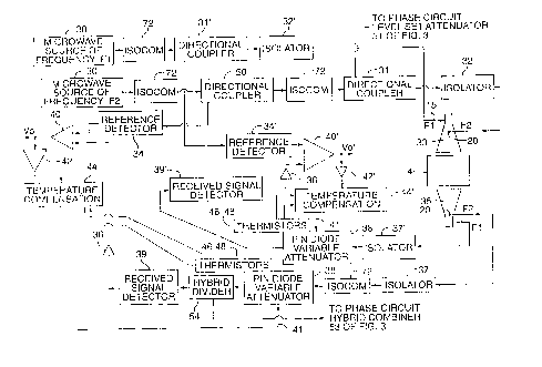
Fig. 2 is a schematic block diagram which shows
the microwave devices and other electronic components in
the preferred embodiment of the microwave measurement
apparatus of the invention, which are used to generate
output signals Vo' and Vo proportional to attenuation of
the microwave beam by the test material for each of the
two frequencies fl and f 2 in accordance with the
formulas:
a~ = Klwd + K2d Equation 6
a = K3wd + K2d Equation 7
Where a', a are the attenuations in decibels for
the two frequencies fl and f2~ and where Kl, K2, K3 are
constants, W is percent water and d is density of the
test material. In Fig. 2, a first microwave source 30'
generates an amplitude modulated microwave signal of a
high frequency fl of, for example 10.7 GHz which passes
through a directional coupler 31' and an isolator 32~ to
connector 15 of a transmitting antenna 33 which is like
antenna 11 in Fig. 1. A second microwave signal source
30 of a lower frequency f 2 Of, for example 5.86 GHz
transmits such signal through two directional couplers
50 and 31 and an isolator 32 to connector 20 of the
transmitting antenna 33. The directional coupler 50
feeds a small part, generally between 0.1~ and 1.0~ of
the signal f 2 to a reference detector 34 which produces a
CA 022l6037 l997-09-l7
~C:tdy 8/29/97 247-44577.app ~ 17 -
reference signal whose amplitude is proportional to the
microwave power passed to the transmitting antenna.
The received microwave signal f2 after passing
through the moist test material 1 is passed from the
connector 20 of a receiving antenna 35 through another
isolator 37 to the input of a PIN diode variable
attenuator 38 which further attenuates the signal to
produce a constant signal level at the input to the
signal detector 39 connected through a hybrid divider 54
to the output of such attenuator. This constance is
achieved by comparing the atteruated received signal
from the signal detector 39 after it is amplified by
preamplifier 36 to equal the reference signal from the
reference detector 34 which are applied to the two
inputs of a high gain differential amplifier 40 to
produce an attenuated output signal, Vo, proportional to
the attenuation of the test material as given in
Equation 7. It should be noted that the preamplifier 36
may be combined as a part of the differential amplifier
40. The output signal, Vo, of differential amplifier 40
is also transmitted through a preamplifier 42 and a
temperature compensation circuit 44 including a pair of
thermistors 46 and 48 to a control terminal 41 of the
attenuator 38, making a closed loop, negative feedback
arrangement. The temperature compensation circuit 44 is
shown in Fig. 11 and operates ina manner hereafter
described to adjust the attenuation characteristic of
the PIN diode attenuator 38 to compensate for
temperature changes, as shown in Fig. 12. As a result
of such negative ~eedback, any difference between the
two compared signals at the inputs of amplifier 40 is
applied to control terminal 41 of attenuator 38 and
causes a change in attenuation of the received signal by
the PIN diode attenuator as needed to bring the
microwave signal level at the input of signal detector
39 to the desired constant value. The same -ircuit
operation occurs when the first microwave signal of high
frequency fl of, for example, 10. 7 GHz is transmitted
CA 02216037 1997-09-17
JC:tdy 8/29/97 247-44577.app - 18 -
from source 30' through coupler 31' and isolator 32' to
the coaxial connector 15 of transmission antenna 33.
Therefore, such operation of the other attenuation
circuit including isolator 37', PIN diode variable
attenuator 38', signal detector 39', preamplifier 36',
reference detector 34', differential amplifier 40',
preamplifier 42' and temperature compensation circuit
44' to produce the second attenuated output signal Vo
will not be described.
Clearly, if there is an increase of attenuation
by the moist test material 1 there will be an equal
decrease of attenuation by the PIN diode attenuators 38
and 38'. Since the attenuation by each PIN diode
attenuator is a direct function of the output signal Vo
or Vo' fed to its control input 41 or 41', these output
signals provide a direct measure of the attenuations "a"
in the moist material at frequencies f2 and f1,
respectively. Thus, the difference between attenuation
a and attenuation a' obtained by subtracting Vo' from Vo
is proportional to the amount of moisture in the test
material.
For phase measurement in Fig. 3 using low
frequency microwave signal f2 to determine the density of
the test material, all the components of the
corresponding circuit of Fig. 2 are used as described
above for attenuation measurement and directional
coupler 31 is employed to provide a phase reference
signal and a hybrid divider 54 is added between the PIN
diode attenuator 38 and the signal detector 39 in
Fig. 2. These two added components are fixed passive
devices so that their addition leaves the operation of
the attenuation loop effectively unchanged.
Fig. 3 is a schematic block diagram of the phase
measuring circuit used in one embodiment of the
invention. Microwave source 30 transmits microwave
signal f2 of low frequency of 5.86 GHz through the
directional coupler 50 and coupler 31 which feeds a
small fraction (between 0.1~ and 1.0~) of the signal
CA 02216037 1997-09-17
JC:tdy 8/29/97 247-44577.app -- 19
through a level set attenuator 51, a fixed attenuator 52
of 21 decibels attenuation and a voltage variable phase
shifter 55 to one input of a hybrid combiner 53 to
provide a phase reference signal to this combiner. The
microwave source 30 is connected to a DC power supply
voltage source 75 of about -12 volts which is battery
operated and is provided with a temperature compensation
circuit 77 including a thermistor 79 mounted in heat
conduction to the microwave signal source to maintain
the frequency of such signal substantially constant by
varying the power supply voltage in response to
temperature changes of the source. Thus an increase in
source temperature causes an increase in source
frequency while an increase in source supply voltages
causes a decrease in source frequency.
On the receiving side, the output of PIN diode
variable attenuator 38 is connected to the input of
added hybrid divider 54 which feeds half the received
signal to the attenuation loop 39, 36, 40, 42, 44 and 41
of Fig. 2 and the other half of such received signal is
fed from divider 54 to one input of a hybrid combiner 53
whose other input i 5 connected to the output of a
voltage variable phase shifter 55.
The voltage variable phase shifter 55 is
arranged to be swept periodically through a full 360~
phase change by the ramp shaped voltage applied to
control terminal 71 by a ramp generator 56. As a
result, the phase of the phase shifted received signal
applied by shifter 55 to the second input to the hybrid
combiner 53 is swept periodically through 360O.
The hybrid combiner 53 of Fig. 3 combines the
two input signals so that its combined output signal is
the vector sum of such two input signals. If,
therefore, the two input signals are of equal amplitude
there will be one point in the 360~ sweep where the two
signals are 180~ out of phase with each other and the
hybrid combiner output will dip to a minimum amplitude.
The operation of the attenuator loop 54, 39, 36, 40, 42,
CA 02216037 1997-09-17
JC:tdy 8/29/97 247-44577.app ~ 20
44, 41 shown in Fig. 2 of attenuator 38 ensures that the
signal level at the output of the attenuator remains
almost constant and is a near constant fraction of the
phase reference output signal of the directional coupler
31. The level set attenuator 51 is therefore adjusted
to make the amplitudes of the two input signals of the
hybrid combiner 53 near to equal. The output from the
hybrid combiner 53 passes through the phase signal
detector 57 which gives a detected output signal whose
amplitude is proportional to the amplitude of the
combined output signal of the hybrid combiner and which
therefore goes through a sharp minimum at one point in
each 360~ sweep of the ramp generator. It should be
noted that each sweep can be less than 360~ if it
includes the sharp minimum. This detected signal is
amplified by amplifier 58, rectified by a full wave
rectifier 59 and filtered by low pass filter 60 to give
a phase shift indication signal 67 at test point No. 1
as shown graphically in Fig. 4. The low pass filter 60
between the rectifier 59 and TP1 serves to clean up this
signal by removing noise and unwanted components from
the signal.
A differentiator circuit 61 converts the signal
from TP1 to the differentiated phase shift indication
signal 68 of the waveform indicated in Fig. 5 at TP2 in
which there is a sharp transition through zero. The
comparator 62 and capacitor 63 serves to convert this
signal into a sharp positive spike pulse 69 at TP3
corresponding to the zero crossing of signal 68 and
applies such spike pulse to one input of the latch 64
and as shown in Fig. 6. The other input of the latch 64
is a second sharp spike pulse corresponding to the start
of the ramp voltage signal 71 which comes from the ramp
generator circuit 56 so that a positive rectangular
latch output pulse 70 produced at TP4 is initiated at
the start of each ramp and is terminated by spike pulse
69 at the phase signal minimum point as shown in Fig. 7.
This is repeated for each repetitive 360~ sweep of the
CA 022l6037 l997-09-l7
JC:tdy 8/29/97 247-44577.app ~ 21 -
ramp generator and so produces a pulse train with pulses
70 of constant amplitudes and variable pulse widths with
their pulse width proportional to the phase shift of the
minimum point in signal 67 corresponding to the output
from the hybrid combiner 53. The integrator 65 which
integrates this pulse train therefore gives a phase
shift output signal, Vp, whose voltage level is
proportional ~o this phase shift.
The phase shift signal Vp is approximately
proportional to the density of the test material in the
following equation for the moisture range of zero to
four percent moisture which applies to foundry sand.
log ~m = ClWd + C2d Equation 8
where ~ is the dielectric constant of the mixture of
air, water and sand in the test material, C1 and C2 are
constants related to the dielectric constants of water
and sand, W is the percent of water and d is the density
of the test material.
The zero level of this phase shift output signal
Vp corresponds to the phase of the received signal which
would produce a hybrid combiner output signal minimum at
the start of each ramp. This can be adjusted to a
desired minimum corresponding, for example, to some
minimum density at zero percent water by adjustment of a
pre-settable phase shifter (not shown) provided at the
input of attenuator 38. The phase shift output signal V
of integrator 65 and the attenuation output signals Vo
and Vo' of the differential amplifiers 40 and 40' of
Fig. 2 are applied to the inputs of a dedicated computer
or data processor 66, such as a general purpose digital
computer, which is programmed to combine such signals in
accordance with Equations 6, 7 and 8 to produce a
percent moisture content signal at the output of such
data processor which indicates the amount of moisture in
the test material 1. The dedicated computer 66 of
CA 022l6037 l997-09-l7
JC:tdy 3/29/97 247-44577.app ~ 22
Fig. 3 provides three functions. First, detailed
operating instructions to the operator who may have no
instrumentation training or experience. This includes
control by the computer of a suitable indicator display
to indicate use of the correct cup size for the
substance being measured in response to the output of a
cup size sensor circuit 135 hereinafter discussed.
Second, control of power supply battery charging.
Third, preset input by software into the computer, of
all formulae or equations and all constants required for
the calculation of the desired output measurement
signals, for each of the test materials. In general
these output measurements relate to "moisture" but may
also include "density" or may include "conductivity",
either ionic or metallic or carbon.
A plurality of microwave connectors 72 each
hereinafter called an "Isocom", are provided at various
positions throughout the microwave circuits of Figs. 2
and 3 to isolate the outer conductors of interconnected
microwave waveguides, such as coaxial cables, from DC
voltage coupling while allowing low impedance AC voltage
coupling of microwave frequency signals. The microwave
connector 72 is shown in the exploded view and the
assembled view of Figs. 13 and 14 and preferably
includes two coaxial cable connectors 73 and 74, such as
SMA type connectors for printed circuit boards. Each of
the connectors 73 and 74 includes an outer conductor 76,
78 and an inner conductor 80, 82 separated by an
insulator sleeve 84, 86 of Teflon or other suitable
plastic. A pair of conductor disks 88, 90 of brass or
other suitable metal are soldered to the mounting
flanges of the outer conductors 76 and 78, respectively,
and may have a diameter of 2.0 cm. The conductor disks
88, 90 are separated by an insulator disk 92 of mica or
other suitable high dielectric material of somewhat
greater diameter than the conductor disks and having a
thickness of about .013" to insulate the conductor disks
from each other. The insulator disk 92 iS provided with
CA 022l6037 l997-09-l7
JC:tdy 8/29/97 247-44577.app ~ 23 -
a central opening 94 therethrough of sufficient diameter
to allow the inner conductor 80 of connector 73 to pass
through such disk and interconnect with the inner
conductor 82 of connector 74 by a plug and socket type
connection and by soldering after assembly or by a
single conductor interconnecting both connectors. After
the microwave connector 72 iS assembled as shown in
Fig. 14 the mechanical contact of the conductor disks
88, 90 with the insulator disk 92 iS maintained by epoxy
10 resin potting material 95 around such disks to provide
the connector with an outer diameter of 3 cm and a
maximum connector length of 1.9 cm. It should be noted
that the outer conductors 73 and 74 are isolated by the
insulator disk 92 to prevent DC voltage coupling between
15 such outer conductors but are capacitively coupled
through such disk to provide a low impedance AC voltage
coupling at microwave frequencies but a high impedance
coupling at lower modulation frequencies. Thus for
brass conductor disks 88, 90 of 2 cm diameter and .016"
20 thickness separated by a mica insulator disk 92 of . 013"
thickness and a dielectric constant of 7, the calculated
capacitance is 50 picofarads. This capacitive
connection had a DC resistance greater _han 10 megohms,
a high AC impedance of 300 kilohms or more at modulation
frequencies of 10 kHz to 20 kHz and low AC impedance of
less than 1 ohm and less than 0. 25 decibel atteluation
of microwave signals in the range of 5. 8 GHz to
10.7 GHz.
The microwave connectors 72 solve the problem of
30 most microwave waveguides which use their outer
conductor both as a metal shield to contain the
microwaves and as a common return or ground return which
therefore interconnects almost all the microwave
components of a circuit. This results in ground loops
for signals of different frequencies and phase with
attendant interference and spurious signal problems. A
portable microwave instrument cannot use separate power
supplies and isolation transformers to solve this
CA 02216037 1997-09-17
.,
JC: tdy 8/29/97 247-44577 . app ~ 24
problem because of the added weight and size and because
it uses a battery power supply.
The temperature compensation circuits 44 and 44'
for the PIN attenuators 38 and 38' of Fig. 2, are shown
in Fig. 11 to each include a first thermistor 46 and a
second thermistor 48 whose resistance varies with
temperature. The input terminal 96 of the circuit 44 is
connected through an input coupling resistor 98 of 301
kilohms to the inverting input of an operational
amplifier 100 with a negative feedback resistance 101 of
100 kilohms and whose non-inverting input is connected
to ground through a bias resistor 102 of 25 kilohms.
The first thermistor 46 is connected in series with a
fixed resistor 104 of 143 kilohms and this series
impedance is connected in parallel with the input
coupling resistor 98. The operating characteristic of
the PIN attenuators 38 and 38' is shown in Fig. 12 by
curves of attenuation in decibels along the vertical
axis and attenuator control voltage at control input 41
along the horizontal axis. As a result of changes in
the resistance of the thermistor 46 with changes in
temperature of the PIN attenuator 38 on which it is
mounted, the slope of the attenuation operating
characteristic curve 106 at 23.7~ C changes as shown by
curves 106A and 106B at 0~ C and 41.5~ C to compensate
for such changes, as shown in Fig. 12.
For the purpose of temperature compensation, the
PIN attenuation curve is approximated by two straight
lines; a short horizontal line 109 representing zero PIN
attenuation, where the PIN control voltage is ~elow the
point where PIN diode current starts, and a rising
sloping straight line 106 of constant slope following
most of the increase of PIN attenuation with increasing
control voltage and control current. Where these two
straight lines intersect is termed the "break point".
The slopes of the three attenuation curves 106, 106A and
106B at different temperature of 23.7~ C, 0~ C and
41.5~ C, respectively, when projected downward intersect
CA 022l6037 l997-09-l7
JC:tdy 8/29/97 247-44577.app -- 25
the horizontal straight line portion 109 at 1 decibel
attenuation which corresponds to "the insertion loss" of
the PIN attenuator, at break points 121, 121A and 121B,
respectively.
A shunt resistance network including a pair of
series connector resistors 108 and 110 of 3.65 kilohm
and 90.9 kilohms, respectively, is connected from the
inverting input of the ampIifier 100 to a source of DC
reference voltage of -5.6 volts at the common connection
10 of Zener diode 114 and resistor 118 of 3.32 kilohms from
l DC voltage source of -15.6 volts. The second
thermistor 48 iS connected in parallel with a resistor
120 of 4.75 kilohms and this parallel impedance is
connected in series with a shunt resistor 122 of 100
15 kilohms from the inverting input of amplifier 100 to a
source of DC reference voltage of +5.6 volts at the
common connection of a Zener diode 112 and a resistor
116 of 3.32 kilohms from a DC voltage source of +15.6
volts. AS a result of changes in the resistance of the
20 second thermistor 48 with changes in temperature of the
PIN attenuator 38 the break voltage point 121 of the
attenuation curve 106 changes from 0. 465 volt as shown
in Fig. 12 to break points 121A and 121B of 0. 510 volt
and 0. 420 volt for attenuator curves 106A and 106B to
compensate for such changes. It should be noted that
the current flowing through the thermistors 46 and 48 iS
small enough to have a negligible effect on their
temperature.
The output of the operational amplifier 100 is
connected through a diode 123 in series with a coupling
resistor 124 of 1. 8 kilohms to the control terminal 41
of the attenuator 38 to change the attenuation in
accordance with the output voltage signal applied to
such control terminal, as shown in Fig. 12. A shunt
capacitor 126 of 0. 47 microfarads is connected from the
output terminal 41 and ground. As shown in Fig. 12
changes in the control voltage applied to the control
input 41 of the attenuator 38 change the attenuation of
CA 02216037 1997-09-17
~JC:tdy a/29/97 247-44577.app - 26 -
the received microwave signal transmitted through such
attenuator.
As shown in Fig. 8 the test container size
sensor includes a container holder which employs a
sensor pattern 128 of conductive strips including a
common input strip 130 and a plurality of insulated
output strips 132. The output strips 132 are
selectively coupled to the input strip 130 through four
different test patterns of conductor strips 134A, 134B,
134C and 134D on the bottoms of the four different si,_
test containers, as shown in Fig. 9. A number of
different size test containers 4 are necessary because
of the wide range of moisture contents to be measured
with high accuracy. Thus .or very wet material a large
container should not be used because of too high
attenuation of the received signal so that its amplitude
is too small or inaccurate for accurate moisture
measurement. On the other hand, for low moisture
material a small container should not be used because of
too little attenuation of the signal.
A test container sensor circuit 135 is shown in
Fig. 10 and includes an AC signal source 136 of 14 to
25 kHz and a peak-to-peak voltage of about 10 volts
which is applied to the input strip 130 of the sensor
pattern 128. The test signal is coupled to the sensor
circuit amplifier 142 by a first effective capacitance
138 between such input strip and the selected container
pattern 134 and by a second effective capacitance 140
between the selected container pattern and the
corresponding output strip 132. The selected container
size signal is transmitted through capacitance 140 to
the inverting input of an operational amplifier 142
whose non-inverting input is connected to ground. A
negative feedback resistor 144 of 3.6 megohms is
connected from the output of the amplifier 142 through
an output coupling diode 146 to the inverting input of
such amplifier. A diode 148 is connected from the
inverting input to the output of amplifier 142 to
CA 02216037 1997-09-17
JC:tdy 8/29/97 247-44577.app ~ 27
discharge the capacitances 138 and 140 through coupling
diode 146. A shunt impedance including a resistor 150
of 68 kilohms and a parallel capacitor 152 of 82
picofarads is connected from the inverting input of
amplifier 142 to ground to reduce stray coupling output
signals. The container sensor output signal is
transmitted from the output of amplifier 142 to an
output terminal 154 through a smoothing filter including
a coupling resistor 156 of 10 kilohms and a shunt
10capacitor 158 of 22 nanofarads. The output terminal 154
of the cup size sensor circuit 135 of Fig. 10 is
connected to the input of the computer 66 of Fig. 3.
There are four of these container size sensor
circuits, one for each of the four container cup sizes
15having signal path lengths of 3", 2", 1", 1/2". When a
cup is installed, the circuit for its size is required
to give an output voltage signal to the computer at
output 154 which will be read as a "high"; this means
that it must be greater than 3 volts. The other three
sensor circuits are each, at the same time, required to
give an output voltage signal which will be read as a
"low" and must be less than 1 volt.
The sensor circuit acts as a "perfect detector"
which, with the capacitor 158 and resistor 156 smoothing
filter, yields a steady DC output voltage to the
computer.
Cl is the effective capacitance 138 between the
center strips of the circuit boards in the cup well and
the cup.
30C2 is the effective capacitance 140 between the
cup size strips of the two circuit boards.
Cl and C2 have effective capacitances given by:
C = 8.85 Ad picofa~ads
CA 02216037 1997-09-17
JC:tdy 8/29/97 247-44577.app ~ 28 -
where A is the area of the coupling strips, d is the
distance between the cup strips and the well strips, and
~ is the dielectric constant of the circuit board
insulating material which separates the cup strips from
the well strips.
The capacitance values of C1 and C2 in the
prototype are 6.5 picofarads each in the cup sensor
circuit for the cup size that has been installed, so
that together they provide an input capacitance "C" of
3.25 picofarads.
During each cycle of the 25 kHz input signal,
this capacitance is charged to the peak negative voltage
by current drawn through the 144 feedback resistor Rf and
is then discharged to the peak positive voltage through
the feedback 148 diode DC. Thus, the charge "q" fed
through Rf effects a voltage change across C equal to the
peak-to-peak input signal "V".
The charge "q" to the capacitance C = 3.25
picofarads with a 10 volt peak-to-peak input signal "V"
is thus:
q = C x V = 32.5 micro micro coulombs
This charge, drawn through the 144 feedback
resistor Rf once every cycle of the 25 kHz input signal,
means that there is a mean current "i" through Rf and
i = q/r = 0.8125 micro Amp
where T iS the period of the input signal, equal to
1/25000; this current "i" will produce a mean smoothed
output voltage signal "E" of:
E = i x Rf = 2.925 volt
CA 022l6037 l997-09-l7
.JC:tdy a/29/97 247-44577.app - 29 -
Due to stray couplings, much of it due to other
stray frequencies, there is a small additional input
signal, other than through Cl and C2. With no cup
installed, this produces an output signal which was
measured to be about 1.3 volt. To reduce this, the
capacitor 152 and the resistor 150 were added to the
sensor circuit at the operational amplifier input; they
have reduced this stray output signal to about 0.45
volt. Since this is present at all times it adds to the
cup signal to yield a total output for the installed cup
of 3.375 volt, which certainly registers as a "high" in
the computer.
In the three sensor circuits for cup sizes other
than the one installed, the input capacitor Cl is still
6.5 picofarads, as for the installed cup, but C2 iS
greatly reduced, both because the installed cup does not
have the cross strips for the other cup sizes and
because of the shielding effect of the grounded
conductors which have been added to the well circuit
board, between all the strips, for this purpose, coupled
with the use of shielded interconnecting leads from the
strips to the cup sensor circuits. The result is that
the net input capacitance to these other sensor circuits
is only about 0.38 picofarads, giving only about 0.34
volt output to combine with the approximately 0.45 volt
due to stray input signals; this gives a net output
signal to the computer of less than 0.8 volt which
certainly registers as a "low".
There was one further problem affecting the cup
sensing. If the material being measured in the cup is
electrically conducting, or has some electrical
conductivity, (as does foundry molding sand, due to
presence in it of free carbon atoms) this could add
appreciable stray couplings between the sensing strips,
causing false cup size signals. The means which has
been found to be effective to obviate this is to add a
spacer between the bottom of the cup and the circuit
board carrying the sensing strips so as to make the
CA 02216037 1997-09-17
~C:tdy a/29/97 247-44577.app - 30 --
distance between the measured material and the sensing
strips at least 3/8".
It will be obvious to those '~aving ordinary
skill in the art that many changes may be made in the
above described preferred embodiment of the present
invention. Therefore, the scope of the present
invention is to be determined by the following claims.