Language selection

Search

Patent 2216136 Summary

Third-party information liability

Some of the information on this Web page has been provided by external sources. The Government of Canada is not responsible for the accuracy, reliability or currency of the information supplied by external sources. Users wishing to rely upon this information should consult directly with the source of the information. Content provided by external sources is not subject to official languages, privacy and accessibility requirements.

Claims and Abstract availability

Any discrepancies in the text and image of the Claims and Abstract are due to differing posting times. Text of the Claims and Abstract are posted:

  • At the time the application is open to public inspection;
  • At the time of issue of the patent (grant).
(12) Patent: (11) CA 2216136
(54) English Title: READ-OUT CIRCUIT FOR ACTIVE MATRIX IMAGING ARRAYS
(54) French Title: CIRCUIT D'EXTRACTION POUR GROUPEMENTS DE PHOTODETECTEURS A MATRICE ACTIVE
Status: Expired and beyond the Period of Reversal
Bibliographic Data
(51) International Patent Classification (IPC):
  • H01L 31/046 (2014.01)
(72) Inventors :
  • WAECHTER, DAVID (Canada)
  • HUANG, ZHONG SHOU (Canada)
(73) Owners :
  • LITTON SYSTEMS CANADA LIMITED
  • IFIRE TECHNOLOGY CORP.
(71) Applicants :
  • LITTON SYSTEMS CANADA LIMITED (Canada)
  • IFIRE TECHNOLOGY CORP. (Canada)
(74) Agent: MARKS & CLERK
(74) Associate agent:
(45) Issued: 2003-09-16
(86) PCT Filing Date: 1995-04-07
(87) Open to Public Inspection: 1996-10-10
Examination requested: 2002-03-12
Availability of licence: N/A
Dedicated to the Public: N/A
(25) Language of filing: English

Patent Cooperation Treaty (PCT): Yes
(86) PCT Filing Number: 2216136/
(87) International Publication Number: CA1995000202
(85) National Entry: 1997-09-22

(30) Application Priority Data: None

Abstracts

English Abstract


Improved circuitry for active matrix image arrays which, in one application
reduces the number of source or gate lines for a given number of pixels, and
in another application extends the dynamic range of the imaging array without
reducing the number of source or gate lines. Each circuit includes multiple
electrodes per pixel and multiple thin film transistors for switching charge
from the pixel electrodes to the data line.


French Abstract

L'invention concerne un circuit perfectionné pour groupements de photodétecteurs à matrice active qui, dans une application réduit le nombre de lignes de source ou de grille pour un nombre donné de pixels, et dans une autre application élargit la plage dynamique du groupement de photodétecteurs sans réduire le nombre de lignes de source ou de grille. Chaque circuit comprend de multiples électrodes par pixel et de multiples transistors à couche mince pour commuter la charge des électrodes de pixel à la ligne de données.

Claims

Note: Claims are shown in the official language in which they were submitted.


11
THE EMBODIMENTS OF THE INVENTION IN WHICH AN EXCLUSIVE
PROPERTY OF PRIVILEGE IS CLAIMED ARE DEFINED AS FOLLOWS:
1. In an imaging array comprising a plurality of pixels
arranged in rows and columns, each of said pixels being
bounded by at least one data line and at least two
control lines connected to a scanning control circuit,
the improvement wherein each of said pixels comprises at
least two pixel electrodes and at least two switching
means, a first one of said pixel electrodes being
connected to said at least one data line via a first one
of said switching means, said first one of said switching
means having a control input thereof connected to a first
one of said control lines for receiving a first scanning
pulse from said scanning control circuit for transferring
charge on said first one of said pixel electrodes to said
at least one data line, a second one of said pixel
electrodes being connected to said first one of said
pixel electrodes via a second one of said switching
means, said second one of said switching means having a
control input thereof connected to a second one of said
control lines for receiving a second scanning pulse from
said control circuit for transferring charge on said
second one of said pixel electrodes to said first one of
said pixel electrodes after said charge on said first one
of said pixel electrodes has been transferred to said at
least one data line.
2. The improvement of claim 1, wherein each of said
switching means further comprises a thin-film-transistor
(TFT).
3. The improvement of claim 2, wherein a source
terminal of said first switching means is connected to
said at least one data line, a gate terminal of said
first switching means is connected to said first one of
said control lines, and a drain terminal of said first

12
switching means is connected to said first one of said
pixel electrodes.
4. The improvement of claim 2, wherein a source
terminal of said second switching means is connected to
said first one of said pixel electrodes, a gate terminal
of said second switching means is connected to said
second one of said control lines, and a drain terminal of
said second switching means is connected to said second
one of said pixel electrodes.
S. A method of operating the imaging array of claim 1,
comprising the steps of:
a) scanning successive ones of said control lines
such that for each of said pixels charge carried by said
first one of said pixel electrodes is transferred to said
at least one data line in response to scanning said first
one of said at least two control lines, and a portion of
charge carried by said second one of said pixel
electrodes is transferred to said first one of said pixel
electrodes in response to scanning said second one of
said control lines;
b) scanning successive ones of said control lines
a second time such that said portion of charge
transferred from said second one of said pixel electrodes
to said first one of said pixel electrodes is transferred
to said at least one data line; and
c) multiplying said portion of charge transferred
to said at least one data line by a correction factor
proportional to capacitance ratio between said first and
second pixel electrodes, whereby each of said pixels
functions as a pixel pair defined by said first and
second pixel electrodes.
6. The method of claim 5, further comprising the steps
of repeatedly further scanning successive ones of said
control lines for clearing charge from said second one of

13
said pixel electrodes.
7. The method of claim 5, further comprising the step
of simultaneously scanning all of said control lines for
clearing charge from said second one of said pixel
electrodes.
8. The improvement of claim 1, wherein said second one
of said pixel electrodes is smaller than said first one
of said pixel electrodes.
9. A method of operating the imaging array of claim 8,
comprising the steps of:
a) scanning successive ones of said control lines
such that for each pixel charge carried by said first one
of said pixel electrodes is transferred to said at least
one data line in response to scanning said first one of
said at least two control lines, and a portion of charge
carried by said second one of said pixel electrodes is
transferred to said first one of said pixel electrodes in
response to scanning said second one of said control
lines;
b) for each of said pixels detecting whether said
charge transferred to said at least one data line is
greater than a predetermined saturation amount;
c) scanning successive ones of said control lines
a further time such that said portion of charge
transferred from said second one of said pixel electrodes
to said first one of said pixel electrodes is transferred
to said at least one data line; and
d) for each of said pixels in which said charge
transferred to said at least one data line is less than
said predetermined saturation amount selecting said
charge for output detection, and for each of said pixels
in which said charge transferred to said at least one
data line is greater than said predetermined saturation
amount multiplying said portion of charge transferred to

14
said at least one data line from said second one of said
pixel electrodes by a correction factor so as to yield an
equivalent charge as stored on said first one of said
pixel electrodes wherein said first and second ones of
said pixel electrodes have identical charge per unit
area, and selecting said equivalent charge for output
detection, thereby extending the dynamic range of said
pixels.
10. In an imaging array comprising a plurality of
pixels arranged in rows and columns, each of said pixels
being bounded by at least one data line and at least two
control lines, the improvement wherein each of said
pixels comprises at least two pixel electrodes and at
least three switching means, a first one of said pixel
electrodes being connected to said at least one data line
via a first one of said switching means, said first one
of said switching means having a control input thereof
connected to a first one of said control lines, a second
one of said pixel electrodes being connected to said at
least one data line via second and third ones of said
switching means, said second one of said switching means
having a control input thereof connected to said first
one of said control lines and said third one of said
switching means having a control input thereof connected
to a second one of said control lines.
11. The improvement of claim 10, wherein each of said
switching means further comprises a thin-film-transistor
(TFT).
12. The improvement of claim 11, wherein a source
terminal of said first switching means is connected to
said at least one data line, a gate terminal of said
first switching means is connected to said first one of
said control lines, and a drain terminal of said first
switching means is connected to said first one of said

pixel electrodes.
13. The improvement of claim 11, wherein a source
terminal of said second switching means is connected to
said at least one data line, a gate terminal of said
second switching means is connected to said first one of
said control lines, a drain terminal of said second
switching means is connected to a source terminal of said
third switching means, a gate terminal of said third
switching means is connected to the second one of said
control lines, and a drain terminal of said third
switching means is connected to said second one of said
pixel electrodes.
14. A method of operating the imaging array of claim 10,
comprising the steps of:
a) scanning successive ones of said control lines
such that for each of said pixels charge carried by said
first one of said pixel electrodes is transferred to said
at least one data line in response to scanning said first
one of said pair of control lines; and
b) scanning successive adjacent pairs of said
control lines a second time such that for each of said
pixels charge carried by said second one of said pixel
electrodes is transferred to said at least one data line
in response to scanning said adjacent pairs of control
lines, whereby each of said pixels functions as a pixel
pair defined by said first and second pixel electrodes.
15. The improvement of claim 10, wherein said second one
of said pixel electrodes is smaller than said first one
of said pixel electrodes.
16. A method of operating the imaging array of claim 15,
comprising the steps of:
a) scanning successive ones of said control lines
such that for each of said pixels charge carried by said

16
first one of said pixel electrodes is transferred to said
at least one data line in response to scanning said first
one of said control lines;
b) for each of said pixels detecting whether said
charge transferred to said at least one data line is
greater than a predetermined saturation amount;
c) scanning successive adjacent pairs of said
control lines a second time such that charge carried by
said second one of said pixel electrodes is transferred
to said at least one data line; and
d) for each of said pixels in which said charge
transferred by said first one of said pixel electrodes to
said at least one data line is less than said
predetermined saturation amount selecting said charge for
output detection, and for each of said pixels in which
said charge transferred by said first one of said pixel
electrodes to said at least one data line is greater than
said predetermined saturation amount multiplying said
charge transferred by said second one of said pixel
electrodes to said at least one data line by a correction
factor proportional to area ratio between said first and
second pixel electrodes and selecting said charge
multiplied by said correction factor for output
detection, thereby extending the dynamic range of each of
said pixels.
17. In an imaging array comprising a plurality of
pixels arranged in rows and columns, each of said pixels
being bounded by a data line and a pair of control lines,
the improvement wherein each of said pixels comprises at
least three pixel electrodes and at least four switching
means, a first one of said pixel electrodes being
connected to said data line via a first one of said
switching means, said first one of said switching means
having a control input thereof connected to a first one
of said control lines, a second one of said pixel
electrodes being connected to said first one of said

17
pixel electrodes via a second one of said switching
means, said second one of said switching means having a
control input thereof connected to the other one of said
control lines, a third one of said pixel electrodes being
connected to said data line via third and fourth ones of
said switching means, said third one of said switching
means having a control input thereof connected to said
first one of said control lines and said fourth one of
said switching means having a control input thereof
connected to the other one of said control lines.
18. The improvement of claim 17, wherein each of said
switching means further comprises a thin-film-transistor
(TFT).
19. The improvement of claim 18, wherein a source
terminal of said first switching means is connected to
said data line, a gate terminal of said first switching
means is connected to said first one of said control
lines, and a drain terminal of said first switching means
is connected to said first one of said pixel electrodes.
20. The improvement of claim 18, wherein a source
terminal of said second switching means is connected to
said first one of said pixel electrodes, a gate terminal
of said second switching means is connected to said other
one of said control lines, and a drain terminal of said
second switching means is connected to said second one of
said pixel electrodes.
21. The improvement of claim 18, wherein a source
terminal of said third switching means is connected to
said data line, a gate terminal of said third switching
means is connected to said first one of said control
lines, a drain terminal of said third switching means is
connected to a source terminal of said fourth switching
means, a gate terminal of said fourth switching means is

18
connected to the other one of said control lines, and a
drain terminal of said fourth switching means is
connected to said third one of said pixel electrodes.
22. A method of operating the imaging array of claim
17, comprising the steps of:
a) scanning successive ones of said control lines
such that for each of said pixels charge carried by said
first one of said pixel electrodes is transferred to said
data line in response to scanning said first one of said
pair of control lines, and a portion of charge carried by
said second one of said pixel electrodes is transferred
to said first one of said pixel electrodes in response to
scanning the other one of said control lines;
b) scanning successive ones of said control lines
a second time such that said portion of charge
transferred from said second one of said pixel electrodes
to said first one of said pixel electrodes is transferred
to said data line;
c) multiplying said portion of charge transferred
to said data line by a correction factor proportional to
capacitance ratio between said first and second pixel
electrodes;
d) scanning successive adjacent pairs of said
control lines a further time such that for each of said
pixels charge carried by said third one of said pixel
electrodes is transferred to said data line in response
to scanning said adjacent pairs of control lines, whereby
each of said pixels functions as two pixel pairs, a first
one of said pixel pairs being defined by said first and
second pixel electrodes and a second one of said pixel
pairs being defined by said first and third pixel
electrodes; and
e) subtracting said portion of charge transferred
to said data line from said charge transferred to said
data line from said third one of said pixel electrodes.

19
23. The improvement of claim 2, 11 or 18, wherein each
said thin-film-transistor (TFT) is a single gate device.
24. The improvement of claim 2, 11 or 18, wherein each
said thin-film-transistor (TFT) is a dual gate device.
25. The improvement of claim 10, wherein said second and
third switching means are integrated as a dual gate
device.
26. The improvement of claim 17, wherein said third and
fourth switching means are integrated as a dual gate
device.
27. A method of operating the imaging array of claim i,
comprising the steps of:
a) scanning successive ones of said control lines
such that for each of said pixels charge carried by said
first one of said pixel electrodes is transferred to said
at least one data line in response to scanning said first
one of said at least two control lines, and charge
carried by said second one of said pixel electrodes is
redistributed to both said first one of said pixel
electrodes and said second one of said pixel electrodes
in response to scanning said second one of said control
lines; and
b) scanning successive adjacent pairs of said
control lines a second time such that all remaining
charge on said first and second ones of said pixel
electrodes is transferred to said at least one data line.
28. In an imaging array comprising a plurality of pixels
arranged in rows and columns, each of said pixels being
bounded by a data line and a pair of control lines, the
improvement wherein each of said pixels comprises at
least four pixel electrodes and at least four switching
means, a first one of said pixel electrodes being

connected to said data line via a first one of said
switching means, said first one of said switching means
having a control input thereof connected to a first one
of said control lines, a second one of said pixel
electrodes being connected to said first one of said
pixel electrodes via a second one of said switching
means, said second one of said switching means having a
control input thereof connected to the other one of said
control lines, a third one of said pixel electrodes being
connected to said data line via a third one of said
switching means, said third one of said switching means
having a first control input thereof connected to-said
first one of said control lines and a second control
input thereof connected to said other one of said control
lines, and a fourth one of said pixel electrodes being
connected to said third one of said pixel electrodes via
a fourth one of said switching means, said fourth one of
said switching means having a control input thereof
connected to the other one of said control lines.
29. The improvement of claim 28, wherein each of said
switching means further comprises a thin-film-transistor
(TFT).
30. The improvement of claim 29, wherein a source
terminal of said first switching means is connected to
said data line, a gate terminal of said first switching
means is connected to said first one of said control
lines, and a drain terminal of said first switching means
is connected to said first one of said pixel electrodes.
31. The improvement of claim 29, wherein a source
terminal of said second switching means is connected to
said first one of said pixel electrodes, a gate terminal
of said second switching means is connected to said other
one of said control lines, and a drain terminal of said
second switching means is connected to said second one of

21
said pixel electrodes.
32. The improvement of claim 29, wherein a source
terminal of said third switching means is connected to
said data line, a first gate terminal of said third
switching means is connected to said first one of said
control lines, a second gate terminal of said third
switching means is connected to said other one of said
control lines, and a drain terminal of said third
switching means is connected to said third one of said
pixel electrodes.
33. The improvement of claim 29, wherein a source
terminal of said fourth switching means is connected to
said third one of said pixel electrodes, a gate terminal
of fourth switching means is connected to said other one
of said control lines, and a drain terminal of said
fourth switching means is connected to said fourth one of
said pixel electrodes.
34. A method of operating the imaging array of claim
28, comprising the steps of:
a) scanning successive ones of said control lines
by first applying a medium level voltage to the control
input of each said first one of said switching means such
that charge carried by said first one of said pixel
electrodes is transferred to said data line for each
addressed pixel and a portion of charge carried by said
second and fourth ones of said pixel electrodes is
transferred to said first and third ones of said pixel
electrodes, respectively, for each pixel adjacent to said
addressed pixel, and thereafter applying a high level
voltage to said control input of said first one of said
switching means and said first control input of said
third one of said switching means such that charge
carried by said third one of said pixel electrodes is
transferred to said data line for each addressed pixel;

22
transferred to said data line for each addressed pixel;
b) scanning successive ones of said control lines
a second time such that said portion of charge
transferred from said second and fourth ones of said
pixel electrodes to said first and third ones of said
pixel electrodes is transferred to said at least one data
line.

Description

Note: Descriptions are shown in the official language in which they were submitted.


CA 02216136 1997-09-22
W O96/31976 . PCT/CAg~ C202
R~n-ouT CIRCUIT FOR ACTIVE MATRIX IMAGING ARRAYS
Fiel~ of the Invention
This invention relates in general to imaging arrays,
and more particularly to im~love~ read-out circuitry
which, in one application, r~ c~C the number of source
or gate lines in the array, and in another application
increases the dynamic range for read-out without reducing
the number of source or gate lines.
Background of the Invention
Imaging arrays are known in the art which comprise a
tr~n~llcD~ for either directly converting incident
radiation to electrical charges, or for converting
incident radiation to light energy (i.e. photons) and
then converting the light energy to electrical charges.
It is also known in the art to connect an active matrix
read-out array to such prior art transducers, for
collecting charges generated by the transducer onto
individual pixels of the active matrix array, and then
reA~; ng out the pixel charges on a row-by-row basis. The
charge signals read out of the array are then measured
using charge amplifiers connected to each source or data
line. Examples of such prior art systems are disclosed
in W. Zhao and J.A. Rowlands, "A Large Area Solid-State
Detector for Radiology Using Amorphous Selenium", in
Medical Imaging VI: Instrumentation, SPIE 1651, 134,
(1992), and in L.E. Antonuk, J. Boudry, W. Huang , D.L.
McShan, E.J. Morton, J. Yorkston, M.J. Longo and
R.A. Street, "Demonstration of Megavoltage and Diagnostic
X-ray Imaging with Hydrogenated Amorphous Silicon
Arrays", Med. Phys. 19, 1455 (1992).
one disadvantage of prior art active matrix readout
arrays is that each pixel is connected to a source line
and a gate line of the associated SWitCh; ng transistor
(e.g. thin film transistor (TFT)). This effectively
reduces the fill factor for each pixel, unless an
.

CA 02216136 1997-09-22
W O96/31976 PCT/CAgv~ 02
additional insulating layer is placed between the source
lines or gate lines and the pixel electrodes.
Another disadvantage of prior art active matrix
readout arrays is that it can be difficult and
occasionally impossible to bond the arrays to external
chips, when the gate our source line pitch is very small.
RQn~ing tech~ology is the main limiting factor in certain
applications like mammography, where a pixel pitch as
small as 50 microns is required. In mammography it is
not possible to reduce the problem by bon~i~g chips to
every second line on both sides, since the active area on
at least one side should be as close as possible to the
chest wall and should not be hon~
A further disadvantage of prior art active matrix
readout arrays is that the charge amplifier design for
such prior art arrays usually suffers from a trade-off
between sensitivity and dynamic range. In particular,
where a charge amplifier has been designed for high
sensitivity in a prior art active matrix read-out array,
such an amplifier is not capable of measuring large
signals due to saturation of the response.
Summary of the Invention
According to the present invention, circuitry is
provided which, in one application, is capable of
reducing by half the number of source lines or gate lines
in an active matrix read-out array, and which, in another
application, maintains the usual number of source lines
~ and gate lines, but is capable of ext~n~i ng the dynamic
range of the charge amplifiers. By reducing the number
of source lines and gate lines, the circuitry of the
present invention enjoys substantially increased fill
factor on a per-pixel basis than prior art designs. The
circuitry of this invention also increases the pitch of
the gate or data lines, so that fewer channels are
required in the peripheral gate drivers or charge

CA 02216136 1997-09-22
.~ ~
WO96/31976 PCT/CA9~/00202
amplifiers and fewer wire bonds to these external devices
are n~ . This results in lower cost and improved
reliability and the ability to provide higher resolution
within a given bond pitch constraint. On the other hand,
when the circuitry of the present invention is operated
~ using the usual number of source and gate lines, ex~n~
dynamic range i8 provided over the prior art while
maint~ining high sensitivity of the charge amplifiers.
Brief Descri~tion of the Drawinas
A detailed description of exemplary embodiments of
the invention is provided below with reference to the
following drawings, in which:
Figure 1 is a block schematic diagram of an active
matrix read-out circuit for a radiation imaging device in
accordance with the prior art;
Figure 2A is a block schematic diagram of an active
matrix read-out circuit with reduced number of source
lines per pixel, according to a first emhoAiment of the
invention;
Figure 2B is a block schematic diagram of an
alternative to the first emho~iment shown in Figure 2B.
Fiaure 3A is a block schematic diagram of an active
matrix read-out circuit with r~llc~A number of gate lines
per pixel, in accor~ with a second ~ ho~iment of the
invention;
Figure 3A is a block schematic diagram of an
alternative to the C~con~ emhoA;ment shown in Figure 3B;
Flgure 4 ls a block schematic diagram of an active
matrix read-out circuit with reduced number of source and
gate lines per pixel, according to a third ~-~ho~; ~nt of
the invention;
Figure Sa is a schematic diagram of a portion of the
Figure 3 and Figure 4 circuits shown in ~ hF-~l outline,
and Figure 5b is an alternative embodiment of said
portion; and

CA 02216136 1997-09-22
W O96/31976 PCT/CAg5/00202
Figure 6 is a schematic diagram of an active matrix
read-out circuit with reduced number of source and gate
lines per pixel, according to a fourth embodiment of the
invention.
DetAiled Descri~tion of the
Preferred Embodiment and of the Prior A~t
In Figures 1-5, common reference numerals are used
to denote circuit elements ~ ~n to each of the Figures.
Figure 1 shows an active matrix circuit for a
radiation imaging device, according to the prior art. In
this device, a trAnC~l7c~ (not shown) ~Vll~ Ls
ele~L~I -gnetic radiation into charge signal. The
transducer can be, for example, a relatively thick (e.g.
500 ~m) layer of amorphous selenium (a-Se) across which a
high voltage may be applied between a top electrode on
one side of the a-Se layer and the pixel ele~L~odes 1 on
the opposite side. Electron-hole pairs are generated in
the a-Se layer in response to incident radiation, and the
charges move toward the two electrodes under the
influence of an electric field established by the high
voltage.
The charge deposited on pixel electrodes 1 is then
read out on a row-by-row basis by -~nc of an array of
thin film transistors (TFTs 3). Successive rows of pixel
electrodes 1 are scAnne~ in response to ~c~nn; ng ~ollL~ol
circuit 5 applying a scAnn; ~g pulse to gate lines 7, to
which the gate electrodes of successive rows of TFTs 3
are connected. Charges stored on each of the scanned
rows of pixel electrodes 1, are applied to adjacent
source or data lines 9 via the drain-source signal path
through the associated TFTs 3. This signal is measured
using charge amplifiers 11 connected to respective data
or source lines 9. The charge amplifiers 11 may be of
st~n~A~d well known design. A multiplexer 13 is used to
select successive ouL~uLs of the charge amplifiers 11.
Additional A/D conversion circuitry (now shown) is

CA 02216136 1997-09-22
W O96/31976 - PCTICA95/00202
provided to convert the sensed charges to digital signals
for further processing, display, etc.
As ~; ~ct7CC~ above, the ocr~lp~ncy of the source or
data lines 9 re~tlc~C the fill factor of each pixel in
such prior art designs, unless an additional insulating
layer is placed between the source lines and the pixel
ele~lGdes 1. Furthermore, the charge amplifiers 11 for
such prior art read-out matrices, usually suffer from a
trade-off between sensitivity and dynamic range since a
charge amplifier which has been designed for high
sensitivity cannot measure large signals due to
saturation of the responce. Also, many wire bond
connections must be made between the pixel array and the
~c~nning control and charge amplifier circuits (usually
lS silicon integrated circuits).
Turning now to Figure 2A, a f irst emhoAiment of the
circuitry according to the present invention is shown.
In this emho~iment, two pixel electrodes are provided for
each space normally occupied by a single pixel in the
prior art. First pixel electrode lA is connected to
source line 9 via first TFT 3A, the gate input of which
is connected to a first one of the control lines 7 on one
side of the pixel. A ~con~ pixel electrode lB is
connected to first pixel electrode lA via second TFT 3B,
the gate input of which is connected to the other control
line 7 for the pixel.
In operation, after radiation-induced charge has
been deposited on pixel electrodes lA and lB, the gate
linQs 7 are se~uentially ~c~nn~, starting at the top and
moving down. When each row 7 is addressed for the first
time, the charge carried on pixel electrodes lA is read
out through the TFTs 3A. The read-out process
_ entarily leaves pixel electrodes lA free of charge.
When the row im~~~i~tely below is addressed, part of the
charge carried by pixel electrodes lB is transferred to
the pixel electrodes lA, through TFTs 3B. This charge is
then read out when TFTs 3A are activated during the

CA 02216136 1997-09-22
W O96/31976 PCT/CAg~ 202
SDcQ~ sll~ceccive scan of gate lines 7.
on the first sl~ccDccive scan of the gate lines 7,
the transfer of charge from pixel electrodes lB to lA is
incomplete. Co~cD~uently, the signal derived from ths
pixel electrodes lB in the ~~~onA seguential scan of gate
lines 7, must be multiplied by a suitable C~L a~Lion
factor. In particular, the ratio of the total charge
initially ;n~llce~ on pixel lB to the charge measured on
the C~con~ scan, is given by (ClA + ClB)/ClA, where ClA
and ClB are the storage capacit~nceC of pixels lA and lB,
respectively.
In order to completely clear the charge from ~ixel
electrodes 18, many successive scans of the gate lines 7
must be performed. Each scan effectively sub-divides the
rem~; n; ng charge between the lA and lB pixel electrodes,
with the component of charge on pixel electrodes lA being
cleared with each scan. As an alternative, a more
effective clearing ~locedu~e can be implemented by
activating all gate lines 7 simultaneously.
According to a further alternative addressing
.~h~- ~, pixels lA are first read by s~ Qcively
addressing gate lines 7 as discussed above, from the top
row down. The charge originally on the pixels lB which
is thereby redistributed between the pixels lA and lB is
then read-out by simultaneously addressing ad~acent gate
lines 7 (i.e. two at a time), starting from the bottom
and moving up. This allows the original charge on the
pixels lB to be read out completely, without the need for
any multiplication factor.
The circuit of Figure 2A can also be used to extend
the dynamic range for charge read-out without changing
the ~ll h~ of pixels per source line. In this case,
pixel electrodes lB are made smaller than pixel
electrodes lA and are placed sufficiently close to pixel
electrodes lA as to effectively sample the same radiation
induced charge. Suitable area ratios lA/lB could be
anywhere from about 2 to 20. In this case, pixel

CA 02216136 1997-09-22
W O 96/31976 PCT/CA9~ 202
electrodes lA and lB are considered to be components of
the same pixel. On the first scan of gate lines 7, the
charges deposited on pixel electrodes lA are read out.
For some of the pixels, this charge may be enough to
saturate the associated charge amplifiers 11. On the
sQcQn~ scan of s~ C~Ccive rowC 7, the charge from the
smaller pixel electrodec lB are sampled, which, in most
cases, does not result in saturation of the ~cociated
charge amplifiers 11. For those pixels which saturate
the charge amplifiers 11 on the first scan, data from the
second scan, multiplied by a suitable factor, is used.
In rare inst~c~C~ the signals on some pixels might be
large enough to saturate the charge amplifiers 11 even on
the second scan. In such cases, a third or fourth scan
can be used to further sub-divide the remaining charge
until it is r~llc~ to a measurable level.
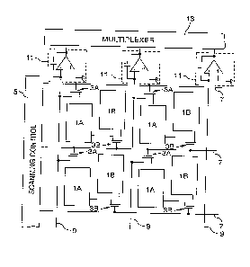
Turning now to Figure 3A, a second embodiment of the
invention is shown in which a given number of pixels are
addressed using only half the usual number of gate lines.
In this emho~; -nt, pixel electrodes lA are
connected to source lines 9 as discussed above with
reference to Figure 2. Second pixel electrodes lC are
also connected to source lines 9, via series-connected
TFTs 3C and 3D, the gate input of TFT 3C being connected
to the top gate line or control line 7, while the gate
input of TFT 3D is connected to the bottom control line
or gate line 7.
In operation; the charge deposited on pixel
electrodes lA are read out by activating gate lines 7 one
row at a time, in the usual -nn~. During this process,
the charges on pixel electrodes lC are not disturbed
since at least one of the two TFTs 3C and 3D will be off
for each pixel. The charges on pixel electrodes lC are
read out only after reading pixel electrodes lA, by
activating two adjacent gate lines 7 simultaneously.
The circuit of Figure 3A can also be used to extend
the dynamic range in a similar manner as discussed above

CA 02216136 1997-09-22
W O96/31976 PCT/CAg~C202
with reference to Figure 2A. In this application, the
pixel electrodes lC are made smaller than pixel
electrodes lA and are placed very close to them, 80 as to
effectively sample the same radiation ;n~ ~ charge.
The signAl~ from pixel electrodes lA are normally used
upon sequential ~~~nn~ng, unles~ saturation of the
associated charge amplifiers 11 occurs. In the latter
case, the signals from the smaller ele~L~odes lC,
multiplied by a suitable correction factor, are used.
With this circuit, only one level of dynamic range
extension is possible since the charges on pixel
electrodes lC are read out completely, rather than being
sub--divided on subsequent scans as in the hoAi -nt of
Figure 2A.
Alternatives to the ~ ho~i ~ts shown in Figures 2A
and 2B are possible. For example, in Figure 2A the
pixels are located to the right of pixels lA and the
number of source lines pwer pixel is reduced. However,
this can be easily rearranged so that the pixels lB are
located beneath the pixels lA as shown in Figure 2B, so
that the 1ll h~ of gate lines per pixel is r~ c~
instead. Likewise in Figure 3B, the pixels lC are shown
disposed to the right of the pixels lA, thereby reducing
the number of source lines per pixel, rather than the
number of gate lines per pixel as in Figure 3A.
The circuits of Figures 2 and 3 can be combined to
reduce both the number of source lines per pixel and the
number of gate lines per pixel, as shown in Figure 4. In
this circuit, pixel electrodes lA are read first by
sequentially sc~nn;ng the gate lines 7 from the top down.
The main portion of charge on pixel electrodes lB is read
next by again sequentially sc~nning the gate lines 7,
from the top down. Finally, pixel electrodes lC are read
by simultaneously addressing adjacent pairs of gate lines
3S 7. The charge measured during this last step will
contain a remnant of charge from pixel electrodes lB.
However, since the magnitude of this charge is known from

CA 02216136 1997-09-22
W O96/31976 PCT/CAg5/00202
the previous step of charge calculation, an equivalent
amount can be subtracted from the charge s~re~ in this
last step by post processing.
In the circuits of Figures 3 and 4, the two
transistors 3C and 3D may be replaced by a single thin
film transistor having both upper and lower gates.
Transistors 3C and 3D, and their alternative dual gate
embodiments are shown in Figures 5a and 5b, respectively.
The alterative embodiment provides an im~ved fill
factor by reducing the number of transistors. In the
alternative embodiment, the gate voltage levels for the
ON and OFF state must be chosen so that transistor 3E is
ON only if both upper and lower gates have ON voltages
applied thereto. In the alternative embodiment,
transistors 3A and 3B can be either single gate devices
or dual date devices, with upper and lower gates
connected together.
Turning now to the alternative embodiment of Figure
6, a fourth pixel electrode lD is provided for each
pixel, this pixel electrode being co~n~cted to pixel
electrode lC via a further TFT switching transistor 3E.
In this ~- ho~ nt, TFT switching transistor 3C' is
fabricated as a dual gate device with top and bottom
gates identified as G1 and G2, wherein the top gate is
physically located above the ~h~nn~l and the bottom gate
is located below the ch~nnel. In operation, the control
lines 7 are successively ~c~nn~ with a two level
waveform, as shown in the left hand portion of Figure 6.
For each col.Lrol line 7 being scanned, a medium level
gate voltage is first applied (e.g. 10 volts from a
nominal OFF value of -5 volts), which causes the charge
collected on pixels lA to be read-out and cleared. The
charges on pixels lC are not transferred at this stage
because the medium level gate voltage is insufficient to
enable transistor 3C' while gate G2 is set to an OFF
(i.e. -5 volts) voltage. The control pulse is then
increased to a high level (e.g. 20 volts), which is

CA 02216136 1997-09-22
W O96/31976 PCT/CA95/00202
cufficient to enable transistor 3C' so that the charge on
pixels lC is read-out, even tholyh the low voltage (e.g -
5 volts) is still applied to gate G2.
This medium-high pulse transition is applied
s~c~ccively to respective ~o..LLol lines 7, preferably
from the top down. During addressing of a subsequent
row, a portion of the charge originally deposited on the
pixels lB is transferred to the pixels lA, and a portion
of the charge originally deposited in the pixels lD is
transferred to the pixels lC. These transferred charges
are then read-out using a second scan of medium-high
pulse transitions, again from the top down.
In order to avoid unwanted mixing of charges, the
transistors 3C' are designed so that they turn on with a
high voltage applied to gate G1 when a low voltage is
applied to gate G2, but are disabled as long as a low
voltage is applied to gate Gl. This characteristic of
the transistors 3C' is ob~; n~ by insuring that the gate
G1 spans the entire length of the ch~nnel, while the gate
G2 spans only a portion of the channel.
The ~ho~l iment of Figure 6 reduces both the n~ h~r
of gates per pixel and the number of source lines per
pixel.
In summary, according to the present invention, a
versatile charge read-out matrix is provided which is
capable in one application of significantly increasing
the pixel fill factor by reducing the number of source
lines and gate lines by one half over known prior art
designs. In another application, the same circuits are
capable of exte~ing the dynamic range of the o~L~L
charge amplifiers without compromising sensitivity.
Alternative embodiments and modifications of the
invention are possible without departing from the sphere
and scope of the invention as defined by the claims
appended hereto.

Representative Drawing
A single figure which represents the drawing illustrating the invention.
Administrative Status

2024-08-01:As part of the Next Generation Patents (NGP) transition, the Canadian Patents Database (CPD) now contains a more detailed Event History, which replicates the Event Log of our new back-office solution.

Please note that "Inactive:" events refers to events no longer in use in our new back-office solution.

For a clearer understanding of the status of the application/patent presented on this page, the site Disclaimer , as well as the definitions for Patent , Event History , Maintenance Fee  and Payment History  should be consulted.

Event History

Description Date
Inactive: IPC expired 2023-01-01
Inactive: IPC removed 2015-05-19
Inactive: IPC assigned 2015-05-19
Inactive: IPC assigned 2015-05-17
Inactive: First IPC assigned 2015-05-17
Inactive: IPC expired 2011-01-01
Inactive: IPC removed 2010-12-31
Time Limit for Reversal Expired 2008-04-07
Letter Sent 2007-04-10
Letter Sent 2005-11-17
Inactive: Late MF processed 2005-10-17
Letter Sent 2005-04-07
Grant by Issuance 2003-09-16
Inactive: Cover page published 2003-09-15
Inactive: Applicant deleted 2003-09-08
Pre-grant 2003-06-11
Inactive: Final fee received 2003-06-11
Notice of Allowance is Issued 2003-01-28
Letter Sent 2003-01-28
Notice of Allowance is Issued 2003-01-28
Inactive: Approved for allowance (AFA) 2003-01-03
Amendment Received - Voluntary Amendment 2002-07-10
Letter Sent 2002-04-16
Request for Examination Received 2002-03-12
Request for Examination Requirements Determined Compliant 2002-03-12
All Requirements for Examination Determined Compliant 2002-03-12
Letter Sent 2000-06-22
Inactive: Inventor deleted 2000-06-06
Inactive: Multiple transfers 2000-05-12
Inactive: Multiple transfers 1998-07-17
Inactive: Single transfer 1998-01-20
Inactive: First IPC assigned 1997-12-10
Classification Modified 1997-12-10
Inactive: IPC assigned 1997-12-10
Inactive: Courtesy letter - Evidence 1997-12-02
Inactive: Notice - National entry - No RFE 1997-11-26
Application Received - PCT 1997-11-25
Application Published (Open to Public Inspection) 1996-10-10

Abandonment History

There is no abandonment history.

Maintenance Fee

The last payment was received on 2003-03-24

Note : If the full payment has not been received on or before the date indicated, a further fee may be required which may be one of the following

  • the reinstatement fee;
  • the late payment fee; or
  • additional fee to reverse deemed expiry.

Patent fees are adjusted on the 1st of January every year. The amounts above are the current amounts if received by December 31 of the current year.
Please refer to the CIPO Patent Fees web page to see all current fee amounts.

Owners on Record

Note: Records showing the ownership history in alphabetical order.

Current Owners on Record
LITTON SYSTEMS CANADA LIMITED
IFIRE TECHNOLOGY CORP.
Past Owners on Record
DAVID WAECHTER
ZHONG SHOU HUANG
Past Owners that do not appear in the "Owners on Record" listing will appear in other documentation within the application.
Documents

To view selected files, please enter reCAPTCHA code :


To view images, click a link in the Document Description column (Temporarily unavailable). To download the documents, select one or more checkboxes in the first column and then click the "Download Selected in PDF format (Zip Archive)" or the "Download Selected as Single PDF" button.

List of published and non-published patent-specific documents on the CPD .

If you have any difficulty accessing content, you can call the Client Service Centre at 1-866-997-1936 or send them an e-mail at CIPO Client Service Centre.

({010=All Documents, 020=As Filed, 030=As Open to Public Inspection, 040=At Issuance, 050=Examination, 060=Incoming Correspondence, 070=Miscellaneous, 080=Outgoing Correspondence, 090=Payment})


Document
Description 
Date
(yyyy-mm-dd) 
Number of pages   Size of Image (KB) 
Representative drawing 1998-01-05 1 7
Representative drawing 2002-11-27 1 8
Description 1997-09-21 10 489
Abstract 1997-09-21 1 45
Claims 1997-09-21 12 500
Drawings 1997-09-21 8 133
Reminder of maintenance fee due 1997-11-25 1 111
Notice of National Entry 1997-11-25 1 193
Courtesy - Certificate of registration (related document(s)) 1998-05-05 1 117
Reminder - Request for Examination 2001-12-09 1 118
Acknowledgement of Request for Examination 2002-04-15 1 180
Commissioner's Notice - Application Found Allowable 2003-01-27 1 160
Maintenance Fee Notice 2005-06-01 1 172
Late Payment Acknowledgement 2005-10-20 1 166
Maintenance Fee Notice 2007-05-21 1 173
PCT 1997-09-21 21 811
Correspondence 1997-12-01 1 30
Fees 2003-03-23 1 53
Correspondence 2003-06-10 1 54
Fees 2002-02-12 1 51
Fees 1998-03-22 1 54
Fees 2001-03-06 1 52
Fees 2004-03-11 1 27
Fees 2006-04-03 1 26