Note: Descriptions are shown in the official language in which they were submitted.
CA 02216296 1997-10-31
--1--
This application is a division of Canadian
Application No. 2,061,499 filed February 19, 1992
for Imaging Method For Manufacture of Microdevices.
FIELD OF THE INVENTION AND RELATED ART
This invention relates generally to an
imaging method for manufacture of microdevices. More
particularly, in one aspect the invention is concerhed
with an imaging method or an illumination method
therefor, suitably usable in forming on a workpiece a
fine pattern of a linewidth of 0.5 micron or less.
The increase in the degree of integration of
a semiconductor device has been accelerated more and
more and, along such trend, the fine processing
techniques have been improved considerably.
Particularly, the optical processing technique which
is major one of them has been advanced to a level of
submicron region, with the start of a l mega DRAN. A
representative optical processing machine is a
reduction projection exposure apparatus, called a
~stepper". It is not too much to say that enh~ncement
of resolution of this apparatus determines the future
of the semiconductor device.
Conventionally, the enhancement of resolution
of the stepper mainly relies on enlarging the N.A.
(numerical aperture) of an optical system (reduction
projection lens system). Since however the depth of
focus of an optical system is in inverse proportion to
the square of the N.A., the enlargement of the N.A.
CA 02216296 1997-10-31
causes an inconvenience of decreased depth of focus.
In consideration of this, attempts have been made
recently to change the wavelength of light for
exposure, from the g-line to the i-line or to excimer
laser light of a wavelength not longer than 300 nm.
This aims at an effect that the depth of focus and the
resolution of an optical system can be improved in
inverse proportion to the wavelength.
On the other hand, in a way separate from
shortening the exposure wavelength, a method using a
phase shift mask has been proposed as a measure for
improving the resolution. According to this method, a
thin film is formed in a portion of a light
transmitting area of a mask which film serves to
provide a phase shift of 180 deg. with respect to the
other portion. The resolution RP of a stepper can be
represented by an equation RP = kl~/N.A., and usually
the stepper has a k1 factor of a level of 0.7 - 0.8.
With the method using such a phase shift mask, the
level of the kl factor can be improved to about 0.35.
However, there remain many problems to
realize such phase shift mask method. Unsolved
problems currently remaining are such as follows:
(1) Satisfactory thin film forming technique for
forming a phase shift film has not yet been
established.
(2) Satisfactory CAD (computer-aided designing)
CA 02216296 1997-10-31
for design of a circuit pattern with a phase shift
film has not yet developed.
(3) Depending on a pattern, a phase shift film
can not be applied thereto.
(4) In respect to the inspection and correction
of a phase shift film, satisfactory technique has not
yet established.
As stated, there remain many problems to
realize a phase shift mask method.
SUMMARY OF THE INVENTION
It is an object of the present invention to
provide a unique and improved imaging method suitable
for manufacture of microdevices such as semiconductor
microcircuit devices.
It is another object of the present invention
to provide a microdevice manufacturing method which
uses such imaging method.
It is a further object of the present
invention to provide an exposure apparatus for
manufacture of microdevices, which uses such imaging
method.
In accordance with a first aspect of the
present invention, there is provided an imaging method
for imaging a fine pattern having linear features
extending along orthogonal first and second
directions, characterized by: providing a light source
CA 02216296 1997-10-31
having decreased intensity portions at a center
thereof and on first and second axes defined to
intersect with each other at the center and defined
along the first and second directions, respectively;
and illuminating the pattern with light from the light
source.
In accordance with a second aspect of the
present invention, there is provided a method of
imaging a fine pattern having linear features
extending in orthogonal first and second directions,
wherein the pattern is illuminated with light
obliquely with respect to the pattern, the
improvements residing in that: the strength of
illumination in a predetermined plane of incidence is
made greater than that in a first plane of incidence
including the first direction and that in a second
plane of incidence including the second direction and
intersecting with the first plane of incidence
perpendicularly.
In accordance with a third aspect of the
present invention, there is provided a method of
imaging a fine pattern having linear features each
extending in a predetermined direction, wherein the
pattern is illuminated with light obliquely with
respect to the pattern, the improvements residing in
that: the illumination of the pattern with light along
a path in a plane of incidence including the
- CA 02216296 1997-10-31
predetermined direction is substantially blocked; and
the pattern is illuminated with light along a pair of
paths which are symmetrical with each other with
respect to the plane of incidence.
In accordance with a fourth aspect of the
present invention, there is provlded an illumination
method in image projection, for illuminating a fine
pattern of an original, characteri~ed by: providing a
light intensity distribution having decreased
intensity portions at a center thereof and on first
and second orthogonal axes with respect to which the
original is to be placed.
These and other objects, features and
advantages of the present invention will become more
apparent upon a consideration of the following
description of the preferred embodiments of the present
invention taken in conjunction with the accompanying
drawings.
BRIEF DESCRIPTION OF THE DRAWINGS
Figure 1 is a schematic view for explaining
the principle of projection of an image of a fine
pattern.
Figures 2A and 2B are schematic views,
respectively, wherein Figure 2A shows a light
distribution as provided on a pupil by diffraction
light from a conventional mask and Figure 2B shows a
CA 02216296 1997-10-31
light distribution as provided on a pupil by
diffraction light from a phase shift mask.
Figures 3A and 3B show a first embodiment of
the present invention, wherein Figure 3A is a
schematic view of an example of effective light source
as formed on a pupil by zero,th order light in the
first embodiment and Figure 3B shows another example
of effective light source as formed on a pupil by
zero-th order light in the first embodiment.
Figure 4 is a graph for explaining frequency
characteristics of a projection system which forms the
effective light source of the Figure 3A example and
that of a projection system of conventional type.
Figures 5A - 5C show a second embodiment of
the present invention, wherein Figure 5A is a
schematic view of a projection exposure apparatus
according to the second embodiment of the present
invention, Figure 5B is a front view of a stop member
used in the second embodiment, and Figure 5C is a
schematic view of a cross filter used in the second
embodiment.
Figures 6A and 6B show a third embodiment of
the present invention, wherein Figure 6A is a
schematic view of a projection exposure apparatus
according to the third embodiment and Figure 6B is a
front view of a stop member used in the third
embodiment.
CA 02216296 1997-10-31
Figure 7 is a fragmentary schematic view of a
projection exposure apparatus according to a fourth
embodiment of the present invention.
Figure 8 is a fragmentary schematic view of a
projection exposure apparatus according to a fifth
embodiment of the present invention.
Figure 9 is a fragmentary schematic view of a
projection exposure apparatus according to a sixth
embodiment of the present invention.
Figure lO is a fragmentary schematic view of
a projection exposure apparatus according to a seventh
embodiment of the present invention.
Figure 11 is a fragmentary schematic view of
a projection exposure apparatus according to an eighth
embodiment of the present invention.
Figure 12 is a fragmentary schematic view of
a projection exposure apparatus according to a ninth
embodiment of the present invention.
Figure 13 is a schematic view of a main
'portion of a projection exposure apparatus according
to a tenth embodiment of the present invention.
Figure 14 is a schematic view for explaining
the relationship between a pupil of a projection
optical system and an optical integrator.
Figures 15A and 15B are schematic views,
respectively,, each showing the pupil of the projection
optical system.
CA 02216296 1997-10-31
Figure 16 is a schematic view of a stop
member usable in the present invention.
Figures 17A and 17B are schematic views,
respectively, each showing the manner of cabling a
mercury lamp.
Figure 18 is a schematic view of a main
portion of a projection exposure apparatus according
to a further embodiment of the present invention.
Figures l9A and l9B are schematic views,
respectively, for explaining the manner of insertion
of a pyramid type prism used in another embodiment of
the present invention.
Figure 20 is a schematic view of a main
portion of a projection exposure apparatus according
to a still further embodiment of the present
invention.
Figure 21 is a schematic view of a main
portion of a projection exposure apparatus according
to a still further embodiment of the present
invention.
Figure 22 is a schematic view of a main
portion of a projection exposure apparatus according
to a yet further embodiment of the present invention.
DESCRIPTION OF THE PREFERRED EMBODIMENTS
For better understanding of the present
invention, description will be made first on details
CA 02216296 1997-10-31
of the imaging of a fine pattern.
Figure 1 shows the principle of image
projection of a fine pattern 6 having a high frequency
(pitch 2d is about several microns), through a
projection lens system 7. The fine pattern 6 which is
illuminated along a direction perpendicular to the
surface thereof, diffracts the light inputted thereto.
Diffraction lights caused thereby include a zero-th
order diffraction light, directed in the same
direction as the direction of advancement of the input
light, and higher order diffraction lights such as
positive and negative first order diffraction lights,
for example, directed in directions different from the
input light. Among these diffraction lights, those of
particular diffraction orders such as, for example,
the zero-th order diffraction light and positive and
negative first order diffraction lights, are incident
on a pupil 1 of the projection lens system 7. Then,
after passing through the pupil 1, these lights are
directed to an image plane of the projection lens
system, whereby an image of the fine pattern 6 is
formed on the image plane. In this type of image
formation, the light components which are
contributable to the contrast of the image are higher
order diffraction lights. If the frequency of a fine
pattern increases, it raises a problem that an optical
system does not receive higher order diffraction
~ ' CA 02216296 1997-10-31
~'
--10--
lights. Therefore, the contrast of the image degrades
and, ultimately, the imaging itself becomes
unattainable.
Figure 2A shows a light distribution on the
pupil 1 in an occasion where the fine pattern 6 of
Figure l is formed on a mask of conventional type,
while Figure 2B shows a light distribution on the
pupil l in an occasion where the fine pattern 6 is
formed on a phase shift mask.
In Figure 2A, about a zero-th order
diffraction light ~a, there are a positive first order
diffraction light 3b and negative first order
diffraction light 3c. In Figure 2B, on the other
hand, due to the effect of a phase shift film a zero-
th order diffraction light 5a is "extinguished" and
there are positive and negative first order
diffraction lights 5b and 5c only. Comparing the
cases of Figures 2~ and 2B, the following two points
may be raised as advantageous effects of a phase shift
mask upon the plane of spatial frequency, i.e., the
pupil plane:
(1) In the phase shift mask, the frequency is
decreased to a half.
(2) In the phase shift mask, no zero-th order
diffraction light exists.
Another point to be noted here may be that
the spacing a between the positive and negative first
' CA 02216296 1997-10-31
order diffraction lights upon the pupil plane in the
case of the phase shift mask corresponds to the
spacing a between the zero-th order light and the
positive (negative) first order diffraction light in
the case of the conventional type mask.
On the other hand, as regards the light
distribution on the pupil l, the conventional type
mask and the phase shift type mask show the same
characteristic in respect to the position. What is
la the difference therebetween is the ratio of intensity
of the amplitude distribution upon the pupil 1. In
the phase shift mask shown in Figure 2B, the amplitude
ratio among the zero-th order, positive first order
and negative first order diffraction lights is O~
whereas in the conventional type mask shown in Figure
2A it is 1:2/~:2/~.
In accordance with one aspect of the present
invention, a light distribution similar to that to be
produced by a phase shift type mask can be produced on
the pupil 1. More specifically, according to this
aspect of the present invention, in order to assure
that, when a fine pattern 6 (more particularly, a fine
pattern as having a spatial frequency that the kl
factor is about 0.5, as suggested in the introductory
part of the Specification) is illuminated, a zero-th
order diffraction light is incident on the pupil l at
a position off the center of the pupil 1 while a
~ ' CA 02216296 1997-10-31
~'
-12-
different diffraction light of higher order is
similarly incident on a position off the center of the
pupil 1, an optical arrangement is provided to produce
such effective light source that: it has a light
quantity distribution in which, as compared with the
light intensity in each of portions on a pair of-axes
passing through the center of the pupil and extending
along longit~ n~l and lateral pattern features of the
fine pattern and as compared with the light
intensity in a portion around the center of the pupil,
the light intensity in a portion other than these
portions is higher. Preferably, there may be produced
an effective light source in which the light intensity
at each of the portions on the pair of axes passing
through the center of the pupil and extending along
the longitudinal and lateral pat_ern features of the
fine pattern as well as the light intensity in the
portion around the center of the pupil, are lowered to
about zero.
When such an effective light source is
provided, of zero-th order and first order diffraction
lights, for example (as produced as a result of
illumination of a fine pattern of a kl factor of about
0.5, for example), the zero-th order diffraction light
and one of the positive and negative first order
diffraction lights may be projected on the pupil l
whereas the other of the positive and negative first
CA 02216296 1997-10-31
order diffraction lights may be prevented from being
projected onto the pupil 1. This assures a light
distribution similar to that to be provided by a phase
shift mask, on the pupil 1.
If in the present invention a single light
beam is used for the illumination, the amplitude-ratio
of a pair of diffraction lights at the pupil 1 becomes
1:2/~, different from a desirable amplitude ratio of
1:1 similar to that as attainable with a phase shift
mask. However, according to the analyses made by the
inventors of the subject application, it has ~een
found that: for resolving a longitudinal pattern
feature of a mask, such a difference in amplitude
ratio can be substantially compensated by using, as
the light to be obliquely projected on the mask (fine
pattern), a pair of lights from a pair of light
sources disposed symmetrically with each other with
respect to a longitudinal axis of the pupil (an axis
passing through the center of the pupil and extending
along the longitudinal pattern feature) so as to
produce on the pupil a pair of light patterns which
are symmetrical with each other with respect to the
longitudinal axis of the pupil; and that for resolving
a lateral pattern feature of the mask, the difference
in amplitude ratio can be compensated by using, as the
light to be projected obliquely on the mask (fine
pattern), a pair of lights from a pair of light
CA 02216296 1997-10-31
-14-
sources disposed symmetrically with each other with
respect to a lateral axis of the pupil (an axis
passing through the center of the pupil, extending
along the lateral pattern feature and being
perpendicular to the longitudinal axis of the pupil)
so as to produce a pair of light patterns which are
symmetrical with each other with respect to the
lateral axis of the pupil.
For resolving a mask pattern having
longitudinal and lateral pattern features, two
illumination light beams, for example, may be used and
projected obliquely to the mask so as to produce an
effective light source having, on the pupil, a light
quantity distribution with a pair of peaks of
substantially the same intensity at those positions:
which are symmetrical with each other with respect to
the center of the pupil, and which are located along a
first axis passing through the center of the pupil and
extending with an angle of about 45 deg. with respect
2~ to the X and Y axes. Also, four illumination light
beams, for example, may be used and projected
obliquely to the mask so as to produce an effective
light source having, on the pupil, a light quantity
distribution with (i) a pair of portions of
substantially the same intensity at those positions:
which are symmetrical with each other with respect to
the center of the pupil, and which are located along a
CA 02216296 1997-10-31
first axis passing through the center of the pupil and
extending with an angle of about 45 deg. with respect
to the X and Y axes and (ii) with a pair of portions
of substantially the same intensity at those
positions: which are symmetrical with each other with
respect to the center of the pupil, which are located
along a second axis passing through the center of the
pupil and extending with an angle of about 90 deg.
with respect to the first axis, and which are at
substantially corresponding locations with respect to
the pair of positions on the first axis and the center
of the pupil.
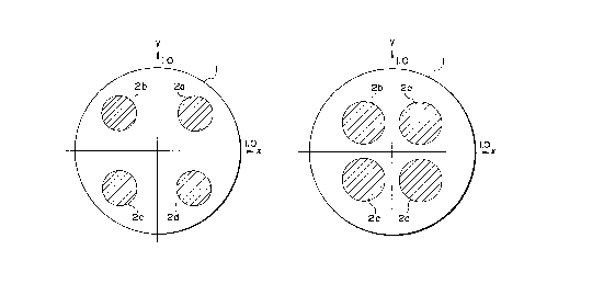
A first embodiment of the present invention
will be explained with reference to Figures 3A and 3B,
wherein Figure 3A shows a light distribution of zero-
th order diffraction light on the pupil 1 of Figure 1,
while Figure 3B shows a distribution of effective
light source on a pupil plane.
In the drawings, denoted at 1 is a pupil;
denoted at x is a lateral axis of the pupil (an axis
passing through the center of the pupil and extending
along a lateral pattern feature); denoted at y is a
longitudinal axis of the pupil (an axis passing
through the center of the pupil, extending along a
longitudinal pattern feature and being perpendicular
to the x axis~; and denoted at 2a, 2b, 2c and 2d are
portions of an effective light source.
CA 02216296 1997-10-31
--16--
In these two examples, the effective light
source has a distribution generally consisting of four
portions. Each portion (light pattern) has a
distribution of circular shape. If the radius of the
pupil 1 is 1.0, the pupil center is at the origin of
coordinate and the x and y axes are the orthogonal
coordinate axes, then in the Figure 3A example the
centers of the portions Za, 2b, 2c and 2d are at the
positions (0.45, 0.45), (-0.45, 0.45), (-0.45, -0.45)
and (0.45, -0.45), and the radius of each portion is
0.2. In the Figure 3B example, the centers of the
portions 2a, 2b, 2c and 2d are at the positions (0.34,
0.34), (-0.34, 0.34), (-0.34, -0.34) and (0.34,
-0.34), and the radius of each portion is 0.25.
The effective light source according to this
embodiment is featurized in that: when the pupil plane
is divided into four quadrants by the x and y axes
defined on the pupil plane, as stated above, each
portion 2a, 2b, 2c or 2d is defined in corresponding
one of the quadrants and also these portions are
defined in a symmetrical relationship and defined
independently of each other, without overlapping.
Here, the x and y axes for the division of the
quadrants correspond to x and y axes, for example,
used for the design of an integrated circuit pattern
and they correspond to the directions of elongation of
longitudinal and lateral pattern features of a mask.
CA 022l6296 l997-lO-3l
--17--
The shape of the effective light source
according to this embodiment is determined in
specific consideration of the directivity of
longitudinal and lateral pattern features of a fine
pattern whose image is to be projected, and it is
featurized in that: the centers of the four circular
portions 2a - 2d are just on + 45 deg. directions
(the directions along a pair of axes passing through
the center of the pupil 1 and extending with angles of
+ 45 deg. with respect to the x and y axes). In order
to produce such an effective light source, a light
source (se~on~ry light source) having the same shape
and the same relationship, with respect to the x and y
axes, as that illustrated may be provided on a plane
optically conjugate with the pupil 1 and four
illumination light beams from the provided light
source may be projected obliquely to a fine pattern at
the same angle of incidence and along two orthogonal
planes of incidence (each two light beams in a pair).
This assures that: linear pattern features extending
along the x axis are illuminated obliquely by the
light beams projected along the paths which are
symmetrical with each other with respect to the plane
of incidence including the x axis; while linear
pattern features extending along the y axis are
illuminated obliquely by the light beams projected
along the paths which are symmetrical with each other
' CA 02216296 1997-10-31
-18-
with respect to the plane of incidence including the y
axis.
It is important that the four portions 2a -
2d of the effective light source have substantially
the same intensity. If the intensity ratio changes,
any defocus of a wafer during the printing thereof,-
for example, causes deformation of the image of a
circuit pattern. ~or this reason, preferably the four
illumination light beams are so set as to provide the
same intensity. As regards the intensity distribution
of each of the four portions 2a - 2d, it may be
determined as desired. For example, it may be a
uniform intensity distribution wherein the whole range
is at a peak level, or it may be a non-uniform
intensity distribution wherein the peak is only at the
center. This means that the four illumination light
beams may take various forms in accordance with the
form of an effective light source to be provided on
the pupil 1. As an example, while in this embodiment
the four portions of th effective light source are
separated from each other and thus no light pattern is
produced in a portion other than the four portions,
the four portions of the effective light source may be
formed to be continuous with the intervention of lower
intensity light patterns.
The distribution (shape) of each of the four
portions 2a - 2d of the effective light source is not
~ ' CA 02216296 1997-10-31
--19--
limited to a circular shape. However, it is desira~le
that, independently of the shape, the centers of the
four portions or the gravity centers of their
intensity distributions are in a symmetrical
relationship and are on the + 45 deg. directions with
respect to the x and y axes, as in the examples of
Figures 3A and 3B.
For further enh~ncement of resolution, i.e.,
in an attempt to adopting an arrangement of an optimum
effective light source adapted to provide a system of
lower kl level, it is seen from the comparison of
Figure 3A with Figure 3B that the gravity center
position of each portion 2a, 2b, 2c or 2d of the
effective light source in each quadrant displaces away
from the center of the pupil 1 and, as a result, the
diameter of each independent portion 2a, 2b, 2c or 2d
in corresponding quadrant decreases.
Illustrated in Figures 3A and 3B are two
types of effective light sources expected. In
practical design, an effective light source similar to
these two types may be used, since, if the gravity
center position of each portion of the effective light
source is too far from the center of the pupil 1, a
problem of decrease of light quantity, for example,
may result (in the respect of convenience in design of
the optical system).
According to the investigations on that point
CA 02216296 1997-10-31
-20-
made by the inventors, it has been found that: in the
coordinate and the pupil 1 shown in Figures 3A and 3B,
if each of a pair of portions 2a and 2c which are in
the first and third quadrants, respectively, and which
S are spaced from each other has a circular shape and a
radius q and if the center positions (gravity center
positions) of the first and second portions 2a and 2c
are at coordinates (p, p) and ~-p, -p), respectively,
then good results are obtainable by satisfying the
following conditions:
0.25 < p < 0.6
0.15 < q < 0.3
It is to be noted that the size and position of each
of the remaining portions 2b and 2d in the second and
fourth quadrants are determined naturally from the
symmetry of them to the portions 2a and 2c in the
first and third quadrants. Also, it has been found
that, even in a case where each portion of the
effective light source has a shape other than a
circular shape, such as, for example, triangular or
rectangular, preferably the above conditions should be
satisfied. In such case, the radius of a circle
circumscribing each portion may be used as the value
of q. In the examples shown in Figures 3A and 3B,
each quantity is near the middle of the range defined
by the corresponding condition. The quantities of p
and q may change in dependence upon a desired
' CA 02216296 1997-10-31
-21-
linewidth of a fine pattern which is required to be
projected by a used optical system (illumination
system/projection system).
In a currently used stepper, an effective
light source has a peak at a center (x, y) = (0, 0) of
a pupil 1. In this type of apparatus, it is said that
the coherence factor (~ level) is 0.3 or 0.5, and this
means that it has an effective light source
distribution having a radius of 0.3 or 0.5 about the
center of the pupil 1. According to the analyses made
by the inventors, it has been found that: if an
effective light source is positioned close to the
pupil center, for example, if the ~ level is in a
range not greater than 0.1, it provides an advantage
that when defocus occurs a high contrast can be
retained mainly in regard to a relatively wide
linewidth (a linewidth to which the above-described k
factor is not less than 1). However, such advantage
as obtainable when defocus occurs diminishes quickly
as the k1 factor becomes close to 0.5. If the k1
factor goes beyond O.S, in a strict case the contrast
of an image is lost fully. What is most required
currently is the improvement in defocus performance at
a kl factor level not greater than 0.6 and, in cases
where the kl factor is at about this level, the
presence of an effective light source adjacent to the
pupil center has an adverse effect on the imaging.
CA 02216296 1997-10-31
-22-
As compared therewith, the effective light
source having been described with reference to the
first embodiment has a small k1 factor. For the
imaging in respect to a kl factor of about 0.5, it
provides an advantageous effect of retaining a high
contrast when defocus occurs. Since in the example
of Figure 3A each of the portions 2a - 2d of the
effective light source is located outwardly, as
compared with those of the Figure ~B example, it
provides a superior high frequency characteristic as
compared with the Figure 3B example. It is to be
noted that, in a portion of the effective light source
spaced away from the pupil center, the defocus
characteristic is such that, up to a kl factor of
about 1, the depth of focus is maintained
substantially at a constant level.
Figure 4 shows the relationship between the
resolution and the depth of focus in a case where the
example of Figure 3B is applied to an i-line stepper
having a N.A. of 0.5, the calculations having been
made on assumption that the defocus in a range
satisfying the contrast of an optical image of 70 % is
within the depth of focus (tolerance). Curve A in the
drawing depicts the relationship between the
resolution and the depth of focus in the case of the
conventional method (~ = 0.5) using a conventional
reticle, while curve B depicts the relationship
CA 022l6296 lss7-l0-3l
between the resolution and the depth of focus in the
case of the Figure 3B example. If the limit of the
depth of focus of a stepper which may be practically
admitted is set to be equal to 1.5 micron, then the
limit of resolution is ~.52 micron in the case of the
conventional method. As compared, in the case of the
~igure 3B example, the resolution is improved to about
0.4 micron. This corresponds to an improvement of
about 30 % in terms of ratio, which is considerably
large in the field to which the present invention
pertains. In effect, a resolution of about 0.45 (k
factor) is easily attainable.
The present invention in this aspect differs
from what can be called a "ring illumination method"
wherein no effective light source is formed at the
pupil center, in that: on the pupil 1, the effective
light source has a peaX neither on the x axis nor on
the y axis correspon~ing to the direction of the
longitudinal pattern feature or the lateral pattern
feature of the fine pattern. This is for the reason
that, if the effective light source has a peak on the
x axis or the y axis, the contrast of an image
degrades largely and thus a large depth of focus is
not obtainable. It has been confirmed that, in
respect to the image projection of a fine pattern
mainly consisting of longitudinal and lateral pattern
features, the present invention assures formation of
CA 02216296 1997-10-31
--24--
an image of improved image quality as compared with
that obtainable by the ring illumination method.
The light quantity (light intensity) in each
principal portion of the effective light source of the
present invention may be either uniform or non-uniform
such as a Gaussian distribution.
Figures 5A, 5B and 5C show a second
embodiment of the present invention and illustrate a
semiconductor device manufacturing exposure apparatus
arranged to project an image of a fine pattern in
accordance with an aspect of the invention.
Denoted in the drawings at 11 is a ultra-high
pressure Hg lamp having its light emitting portion
disposed at a first focal point of an elliptical
mirror 12; denoted at 14, 21, 25 and 27 are deflecting
mirrors;and l denoted at 15 is an exposure control
shutter. Denoted at 105 is a field lens; denoted at
16 is a wavelength selecting interference filter;
denoted at 17 is a cross ND (neutral density) filter;
denoted at 18 is a stop member having a predetermined
aperture; denoted at l9 is an optical integrator
having its light receiving surface disposed at a
second focal point of the elliptical mirror 12; and
denoted at 20 and 22 are lenses of a first imaging
lens system (20, 22). Denoted at 23 is a half mirror;
denoted at 24 is a masking blade device having a
rectangular aperture for defining a region of
CA 02216296 1997-10-31
--25--
illumination on a reticle; denoted at 26 and 28 are
lenses of a second imaging lens system (26, 28); and
denoted at 30 is a reticle having formed thereon an
integrated circuit pattern mainly consisting of
longitudinal and lateral pattern features (grid-like
linear features) of a minimum linewidth of about 2
microns. Denoted at 31 is a reduction projection lens
system for projecting the circuit pattern of the
reticle 30 in a reduced scale of 1:5; denoted at 32 is
a wafer coated with a resist; denoted at 33 is a wafer
chuck for holding the wafer 32 by attraction; and
denoted at 34 is an X-Y stage for supporting the wafer
chuck 33 and being movable in x and y directions of an
X-Y coordinate system defined in the exposure
apparatus in relation to the X-Y stage. Denoted at 35
is a glass plate having formed thereon a light
blocking film with an aperture 35a at its center;
denoted at 36 is a casing having an aperture formed in
its top surface; denoted at 37 is a photoelectric
2~ converter provided in the casing 36; and denoted at 38
is a mirror which is a component of a laser
interferometer (not shown) for measuring the amount of
movement (x axis) of the wafer stage 34. Denoted at
40 is a light blocking plate having a predetermined
aperture, which is disposed at a position optically
equivalent to the light receiving surface of the blade
24 so that, like the blade 24, the light beams
CA 02216296 1997-10-31
-26-
emanating from the lenses of the optical integrator 19
are overlapped one upon another on the plate 40.
Denoted at 41 is a condensing lens for collecting
light passed through the aperture of the light
blocking plate 40; and denoted at 42 is a quartered
detector.
As is well known in the art, usually a
circuit pattern of a reticle (mask) is designed with
reference to orthogonal axes (coordinates) so that
longitudinal pattern features and lateral pattern
features of the pattern extend along these axes,
respectively. When such a reticle is introduced into
a projection exposure apparatus, the reticle is placed
on a reticle stage with reference to x and y axes of
an X-Y coordinate system defined in the exposure
apparatus, with the orthogonal design axes of the
reticle placed exactly or substantially aligned with
the x and y axes of the exposure apparatus. Also, the
the X-Y stage on which a wafer is placed has an X-Y
coordinate system with x and y axes along which the X-
Y stage is movable. These x and y axes of the X-Y
stage are designed to be exactly or substantially
corresponds to the x and y axes of the exposure
apparatus. Thus, when a reticle is placed in the
exposure apparatus, usually the directions of
longitudinal and lateral pattern features of the
reticle are placed in exactly or substantially
-
CA 02216296 1997-10-31
alignment with the x and y axes defined in the
exposure apparatus, respectively, or with the x and y
axes along which the X-Y stage moves.
A structural feature of this apparatus
resides in the filter 17 and the stop member 18
disposed in front of the integrator 19. As show~ in
Figure 5B, the stop member 18 comprises an aperture
stop with a ring-like aperture, for blocking the light
near the optical axis of the apparatus, and it serves
to define the size and shape of an effective light
source on the pupil plane of the projection lens
system 31. The center of the aperture is aligned with
the optical axis of the apparatus. On the other hand,
as shown in Figure SC, the filter 17 comprises four ND
filters which are disposed, as a whole, in a cross-
like shape. These four ND filters serve to attenuate
the intensity of light, projected to four zones in the
ring-like aperture of the stop member 18, by 10 - lOO
%. These four zones correspond respectively to the
portions on the pupil plane of the projection lens
system 31 which portions include four points on the x
and y axes corresponding respectively to the
directions of the longitudinal and lateral pattern
features of the reticle 30. By means of this filter
17, the light intensity at the central portion of a
secondary light source as formed at the light emitting
surface of the integrator 19 as well as the light
' CA 02216296 1997-10-31
.'
-28-
intensity along the x and y axes, intersecting with
each other at the center of the secondary light
source, are attenuated and, as a result, the light
intensity of the effective light source along the x
and y axes on the pupil plane of the projection lens
system 31 is attenuated.
The reticle 30 is held on a reticle stage,
not shown. The projection lens system 31 may be
designed with respect to light of i-line (wavelength
365 nm) as selected by the filter 16. The first and
second imaging lens systems (20, 22; 26, 28) are so
set as to place the light emitting surface of the
integrator 19 and the pupil plane of the projection
lens system 31 in an optically conjugate relationship,
while the second imaging lens system (26, 28) is so
set as to place the edge of the aperture of the blade
device 24 and the circuit pattern of the reticle 30 in
an optically conjugate relationship. The blade device
24 comprises four light blocking plates each having
a knife-edge like end and each being movable
independently of the others so as to allow adjustment
of the size of the aperture in accordance with the
size of the integrated circuit pattern on the reticle
30. The position of each light blocking plate is
controlled in response to a signal from a computer
(not shown) provided for the overall control of the
apparatus, and the size of the aperture is optimized
CA 02216296 1997-10-31
-29-
to the reticle 30 used. While not shown in the
drawings, the exposure apparatus is equipped with a
reticle alignment scope to be used for aligning the
reticle 30 with respect to the exposure apparatus as
well as an off-axis alignment scope disposed beside
the projection lens system 31, for aligning the wafer
32 with respect to the reticle ~0.
The half mirror 23 serves to reflect a
portion of light from the integrator 19, and the
reflected light is projected through the aperture of
the light blocking plate 40 and is collected by the
condensing lens 41 upon the quartered detector 42.
The detector 42 has a light receiving surface disposed
to be optically equivalent to the pupil plane of the
projection lens system 31, and a ring-like effective
light source as formed by the stop member 18 is
projected on this light receiving surface. Each
detector section of the detector 42 produces a signal
corresponding to the intensity of light impinging on
the surface of that section. By integrating the
output signals of the sections of the detector 42, an
integration signal for the opening/closing control of
the shutter 15 is obtainable.
The components 35 - 37 disposed on the X-Y
stage 34 provide a measuring unit for examination of
the performance of the illumination system above the
reticle 30. For the examination of the illumination
' CA 02216296 1997-10-31
-30-
system, the X-Y stage 34 moves to a predetermined
position to place the measuring unit at a position
just below the projection lens system 31. In this
measuring unit, light emanating from the illumination
system and reaching the image plane of the projection
lens system 31 is directed through the aperture 35a of
the glass plate 35 and the aperture of the casing 36
to the photoelectric converter 37. The light
receiving plane of the aperture 35a is placed at the
image plane position of the projection lens system 31
and, if necessary, by using an unshown focus detecting
system (a sensor of well known type, for detecting the
level of the wafer 32 surface) as well as a measuring
unit provided in the X-Y stage 34, the level of the
aperture 35a in the direction of the optical axis of
the apparatus may be adjusted. The glass plate 35 is
attached to the casing 36, and the casing 36 has
formed therein an aperture as described. In this
example, the measuring unit is so arranged that the
aperture of the casing 36 is displaceable to the
aperture of the glass plate by a predetermined amount.
The aperture of the casing 36 is placed at such
location at which the N.A. at the image plane side of
the projection lens system 31 is large and also which
is spaced sufficiently from the image plane. As a
result, at the light receiving plane of the aperture
of the casing 36, the same light distribution as
CA 02216296 1997-10-31
provided on the pupil plane of the projection lens
system 31 is produced. In this embodiment, such
measuring unit is not used. How the measuring unit is
to be used will be described later with reference to
an embodiment to be described hereinafter.
In this embodiment: through the functio~ of
the filter 17 and the stop member 18, an effective
light source having a generally ring-like shape but
having decreased intensity portions, including four
zones on the x and y axes corresponding to the
directions of the longitudinal and lateral pattern
features of the reticle 30, as compared with the
intensity of the other portions, is defined on the
pupil plane of the projection lens system 31 by means
of the illumination system (11, 12, 14, 15, 105, 16,
17, 18, 19, 20, 21, 22, 23, 24, 25, 26, 27 and 28),
the circuit pattern of the reticle 30 is illuminated
with uniform illll~in~nce; and an image of the circuit
pattern is projected by the projection lens system 31
upon the wafer 32, whereby the image of the circuit
pattern is transferred (printed) onto the resist of
the wafer 32. The effect of such projection exposure
is as has been described hereinbefore and, with light
of i-line, a fine pattern of 0.4 micron can be
recorded on the resist of the wafer 32 sharply and
stably.
While in this example the filter 17 and the
' CA 02216296 1997-10-31
stop member 18 are disposed in front of the integrator
19, they may be disposed just after the integrator,
particularly at a location which is optically
conjugate with the pupil plane of the projection lens
system 31. Further, a stop member 18 which is shown
in Figure 6B and is used in a third embodiment, to be
described later, may be used in substitution for the
filter 17 and the stop member 18.
Figures 6A and 6B show a third embodiment of
the present invention which is another example of
semiconductor device manufacturing projection exposure
apparatus wherein an image of a fine pattern is
projected in accordance with a method of the present
invention.
In the drawings, corresponding elements or
those elements having corresponding functions as those
in Figures 5A - 5C, are denoted at the same reference
numerals. Comparing the apparatus of this embodiment
with that of Figures ~A - 5C, the former differs from
the latter in that: as shown in Figure 6B, the
aperture of the stop member 18 comprises four separate
apertures; in place of the cross ND filter, four
separate filters 17a, 17b, 17c and 17d corresponding
respectively to the separate apertures of the stop
member 18 are used; and a pyramid-like prism 13 is
inserted between the mirrors 12 and 14.
In this embodiment, the output of the
CA 02216296 1997-10-31
;
guartered detector 42 is used not only for the
opening/closing control of the shutter lS but also for
a different purpose or purposes. ~dditionally, the
measuring unit (35 - 37~ is used.
Now, referring mainly to the differences of
the present embodiment to the preceding embodiments;
advantageous features of the present embodiment will
be explained.
If the integrator 19 is illuminated with
light from the ~g lamp 11, without using the prism 13,
the filters 17a - 17d and the stop member 18, then a
secondary light source having a light quantity
distribution, like a Gaussian distribution, with a
high peak at its center is formed on the light exit
1~ surface of the integrator 19. Since the light exit
surface of the integrator is optically conjugate with
the pupil plane of the projection lens system 31, an
effective light source having a peak of light quantity
distribution, at the center of the pupil, is formed on
this pupil plane. As described hereinbefore, the
effective light source to be used in this aspect of
the present invention is one as havin~ a light
quantity distribution with no peak at the pupil center
and, therefore, it is necessary to block the light
impinging on a portion about the center of the
integrator 19. If, however, the stop member 18 is
disposed simply in front of the integrator 19, a large
CA 02216296 1997-10-31
-34-
portion of the light from the Hg lamp is intercepted
and thus the loss of light quantity is large. In
consideration thereof, in the present embodiment the
pyramid-like prism 13 is interposed just after the
elliptical mirror 12 to control the illuminance
distribution on the optical integrator 19.
The Hg lamp 11 is so disposed that its light
emitting portion coincides with the first focal point
position of the elliptical mirror 12, and the light
emanating from the Hg lamp 11 and reflected by the
elliptical mirror 12 is transformed by the prism 13
into four light beams deflected in different
directions. These four light beams are reflected by
the mirror 14 and reach the position of the shutter
15. If the shutter 15 is open, the light ~eams are
incident on the filter 16. By this filter 16, the i-
line component is selected out of the emitted light
spectrums of the Hg lamp 11, for ensuring the best
performance of the projection lens system 31 for the
2~ projection of an image of the reticle 31 on a resist
(photosensitive layer) of the wafer 32.
The four light beams from the filter 16 pass
through the field lens 105 and then impinge on the
filters 17a - 17d, respectively, which are important
components of this embodiment. These four filters
serve as a correcting means for making the light
quantities of the four light beams substantially
CA 02216296 1997-10-31
\
uniform to thereby correct the symmetry in light
quantity of four portions of the effective light
source as formed on light exit surface of the
integrator 19 and thus that as formed on the pupil
plane of the projection lens system 31. If adjustment
of the light quantity attenuating function of each
filter is desired, different types of ND filters may
be prepared for each filter so that they may be used
selectively. Alternatively, each filter may be
provided by an interference filter and, by utilizing
the band narrowness of the interference filter, the
interference filter may be tilted to effect the
adjustment.
The stop member 18 receives the four light
beams from the filters 17a - 17d. As shown in Figure
6B, the stop member 18 has four circular apertures
which correspond to the four light beams from the
filters 17a - 17d, in a one-to-one relationship.
Thus, the integrator 19 is illuminated with four light
beams from the four apertures of the stop member 18,
whereby an effective light source such as shown in
Figure 3A and corresponding to the apertures of the
stop member 18, is formed on the light exit surface of
the integrator 19 and thus on the pupil plane of the
projection lens system 31.
Usually, the apertures of the stop member 18
each may have a shape corresponding the outer
CA 02216296 1997-10-31
--36--
configuration of each of small lenses constituting the
integrator l9. If, therefore, each small lens of the
integrator has a hexagonal sectional shape, each
aperture may be formed with a hexagonal shape like the
sectional shape of the small lens.
The light from the optical integrator lg goes
by way of the lens 20, the mirror 21, the lens 22 and
the half mirror 23 to the blade device 24. Here, the
light beams from the lenses of the integrator 19 are
superposed one upon another on the plane of the blade
device 24, whereby the blade device 24 is illuminated
with uniform illll~in~nce. Also, the half mirror 23
serves to reflect a portion of each light beam from
each lens of the integrator l9, and the light blocking
plate 40 is illuminated with the reflected light.
Light passing through the aperture of the light
blocking plate 40 is collected by the lens 41 on the
quartered detector 42.
The light passing through the aperture of the
blade device 24 is directed by the mirror 25, the lens
26, the mirror 27 and the lens 28 to the reticle 30.
Since the aperture of the blade device 24 and the
circuit pattern of the reticle 30 are in an optically
conjugate relationship, the light beams from the
lenses of the integrator l9 are superposed one upon
another, also on the reticle 30. Thus, the reticle 30
is illuminated with uniform illuminance, and an image
CA 02216296 1997-10-31
of the circuit pattern of the reticle 30 is projected
by the projection lens system 31.
The detector sections of the quartered
detector 42 correspond respectively to four separate
portions of the effective light source such as shown
in Figure ~A, and each section is able to detect the
light quantity in each corresponding portion
independently of the others. By combining the outputs
of all the sections, the opening/closing control for
the shutter 15 can be effected, as described
hereinbefore. On the other hand, by mutually
comparing the outputs of the sections, any unbalance
in proportion of the light quantities at the
respective portions of the effective light source can
be checked. Here, calibration among the detector
sections of the quartered detector 42 is effective for
enhanced reliability of the unbalance check. Such
calibration will be described later.
The shape of the effective light source
formed on the pupil plane of the apparatus corresponds
to the shape of the integrator 19. Since the
integrator 19 itself is provided by a combination of
small lenses, in a microscopic sense the light
quantity distribution of the effective light source
comprises a combination of discrete ones each
corresponding to the shape of each lens, However, in
a macroscopic sense, a light quantity distribution
CA 02216296 1997-10-31
-38-
such as shown in Figure 3A is provided.
In this embodiment, the light quantity
monitor means (23 and 40 - 42) and the measuring unit
(35 - 37) are used to check the light quantity
distribution of the effective light source. To this
end, the X-Y stage 34 is moved to place the measuring
unit (35 - 37) to a position just below the projection
lens system 31. In this measuring unit, light
emanating from the illumination system and reaching
the image plane of the projection lens system 31 is
directed through the aperture 35a of the glass plate
35 and the aperture of the casing 36 to the
photoelectric converter 37. The light receiving plane
of the aperture 35a is placed at the image plane
position of the projection lens system 31. The glass
plate 35 is attached to the casing 36 and, as
described, the casing 36 has an aperture at a center
thereof. In this example, the measuring unit is so
arranged that the aperture of the casing 36 is
displaceable to the aperture of the glass plate 35 by
a predetermined amount. When illumination is provided
with the illumination system of this embodiment, on
the top of the casing 36, four portions of an
effective light source such as shown in Figure 3A are
provided. The size and shape of the aperture of the
casing 36 can be changed, as the aperture of the blade
device 24. By changing the size and/or the shape of
-
CA 02216296 1997-10-31
-39-
the aperture by means of a driving system (not shown),
it is possible to detect each of the four portions of
the effective light source independently of the others
or, alternatively, it is possible to detect the four
portions of the effective light source at once. On
the other hand, the photoelectric converter 37 has a
light receiving portion of an area sufficient to
receive all the light passing through the aperture 35a
of the glass plate 35. If the area of the light
receiving portion of the photoelectric converter 37 is
too large and the response characteristic of the
electrical system degrades, a condensing lens may be
inserted between the glass plate 35 and the
photoelectric converter 37 to collect the light from
the aperture 35a of the glass plate 35. This is
effective to reduce the area of the light receiving
portion of the photoelectric converter 37 to thereby
improve the response characteristic. Further, if
desired, the uniformness of the illuminance on the
image plane can be measured by moving the X-Y stage 34
along the image plane while holding the aperture of
the casing 36 in a state for concurrent detection of
all the four portions of the effective light source.
The result of measurement of the light
quantity (intensity) in each portion of the effective
light source obtained through cooperation of the
movement of the casing 36, is compared with an output
CA 02216296 1997-10-31
-40-
of c~rresponding one of the detector sections of the
quartered detector 42 at the illumination system side.
Namely, the photoelectric converter 37 at the X-Y
stage 34 side is used as a reference detector for
calibration of the output of the quartered detector
42. This allows stable monitoring any change with
time of the effective light source. Then, any
unbalance in light quantity of the portions of the
effective light source can be detected by means of the
quartered detector 42 or the photoelectric converter
37, and light quantity matching of the portions of the
effective light source can be done by using the
filters 17a - 17d.
In this embodiment: through the function of
the stop member 18 shown in Figure 6B, an effective
light source not having any peak of light quantity
distribution on the x or y axis, corresponding to the
directions of the longitudinal and lateral pattern
features of the reticle 30, or at the pupil center
(optical axis), is defined by zero-th order light on
the pupil plane of the projection lens system 31,
while on the other hand, by means of the illumination
system (11, 12, 13, 14, 15, 16, 17, 18, 19, 20, 21,
22, 23, 24, 25, 26, 27 and 28), the circuit pattern of
the reticle 30 is illuminated with uniform
illuminance. Thus, an image of the circuit pattern is
projected by the projection lens system 31 upon the
CA 02216296 1997-10-31
-41-
wafer 32, whereby the image of the circuit pattern is
transferred to the resist of the wafer 32. The effect
of such pro~ection exposure is as has been described
hereinbefore with reference to Figures 3 and 4 and,
with the use of light of i-line, a fine pattern of 0.4
micron can be recorded on the resist of the wafe~ 32
sharply and stably.
Figure 7 is a fragmentary schematic view of a
fourth embodiment of the present invention, which is
an improved form of the semiconductor device
manufacturing projection exposure apparatus of Figure
6. The elements of Figure 7 corresponding to the
Figure 6 embodiment are denoted by the same reference
numerals as of Figure 6.
In the drawing, denoted at 11 is a ultra-high
pressure Hg lamp, and denoted at 12 is an elliptical
mirror. In this example, light emanating from the
- elliptical mirror 12 is divided by a combination of
beam splitters (51 - 53). More specifically, in order
to provide an effective light source having four
portions such as shown in Figure 3A, the light
emanating from the elliptical mirror 12 is divided
sequentially by means of a first beam splitter 51 and
a second beam splitter 53. Denoted at 52 is a
deflecting mirror for deflecting the light path. The
second beam splitter 53 is disposed obliquely across
the light paths of the two light beams as divided by
CA 02216296 1997-10-31
--42--
the first beam splitter 51, and it serves to divide
each of the two light beams advancing along the sheet
of the drawing and to deflect a portion of each of the
two light beams in a direction perpendicular to the
sheet of the drawing. The remaining portion of each
of the two light beams, not deflected, goes along the
sheet of the drawing, as illustrated. A mirror
optical system (not shown) is disposed on the path of
that portion of light as deflected by the second beam
splitter 53, and it serves to reflect and direct that
portion of light along a path parallel to the path of
light not deflected by the second beam splitter. In
this manner, by means of the beam splitters 51 and 53
and the mirror 52 as well as the unshown mirror
optical system, the light path is divided into four
light paths. These light paths are then combined so
as to form a secondary light source with a light
distribution such as shown in Figure 3A, on the light
exit surface of the integrator 19. As a result, on
the pupil plane of the projection lens system 31, an
effective light source such as shown in Figure 3A is
formed.
On the two divided light paths which are
present on the sheet of the drawing, relay lenses 61a
and 61a are disposed, respectively. These relay
lenses 61a and 62a serves to collect the light beams,
advancing along the respective paths, on the
CA 02216296 1997-10-31
-43-
integrator 19. Since the insertion of the first beam
splitter causes a difference in optical path length
between these two light paths, the relay lenses 61a
and 61b are slightly different from each other in
respect to the structure and the focal length. This
is also the case with an additional pair of relay
lenses (not shown) which are disposed on the pair of
light paths, not shown in the drawing.
Denoted at 63 is a shutter which can be
controlled (opened/closed) for each of the four light
beams provided by the beam splitters 51 and 53.
Denoted at 16a and 16b are wavelength selecting
filters disposed on the two divided light paths,
respectively, which are present on the sheet of the
drawing. While not shown in the drawing, similar
filters are disposed on the two light paths which are
- not on the sheet of the drawing. These filters each
serves to extract the i-line component out of the
light from the Hg lamp, as the filter 16 of the
preceding embodiment. Denoted at 17a and 17b are
filters disposed on the two divided paths in the sheet
of the drawing, each for adjusting the light quantity
in a corresponding portion of the effective light
source. Similar filters are disposed on the two light
paths not included in the sheet of the drawing. These
filters have a similar function as of the filters 17a
- 17d of the preceding embodiment.
CA 02216296 1997-10-31
-44-
In this embodiment, the light path to the
integrator is divided into four and, for this reason,
the integrator is provided by a combination of four
small integrators. Because of the relationship of
superposition of light paths, only two integrators l9a
and l9b are illustrated in the drawing. Since the
structure after the integrators is similar to that of
the preceding embodiment, further description will be
omitted for simplicity.
Figure 8 is a fragmentary schematic view of a
fifth embodiment of the present invention, showing a
semiconductor device manufacturing projection exposure
apparatus wherein an image of a fine pattern is
projected in accordance with a method of the present
invention.
In the apparatus of this embodiment, the
position of an effective light source is changed with
time to thereby form an equivalent effective light
source as of that shown in Figure 3A is formed on the
pupil plane, and the image of a circuit pattern is
projected. In Figure 8, the elements corresponding to
those of the preceding embodiments are denoted by the
same reference numerals. Thus, denoted at ll is a
ultra-high pressure Hg lamp; denoted at 12 is an
elliptical mirror; denoted at 14 is a deflecting
mirror; denoted at lS is a shutter; denoted at l~ is a
wavelength selecting filter; and denoted at l9 is an
CA 02216296 1997-10-31
-45-
optical integrator. The unshown portion, after the
projection lens system 31, has the same structure as
of the preceding embodiments.
An important feature of this embodiment
resides in that a flat parallel plate 71 which is
movable with time is disposed after the integratoT 19.
The parallel plate 71 is disposed obliquely to the
optical axis of the illumination optical system, and
it is swingable to change the angle with respect to
the optical axis, as illustrated, to shift the optical
axis. This means that, if the integrator 19 is
observed through the flat parallel plate 71, from the
reticle 30 side, the integrator 19 appears moving up
and down or left and right with the swinging movement
of the parallel plate 71. In this example, the
parallel plate 71 is so supported that it can be moved
also rotationally about the optical axis. Therefore,
by rotationally moving the parallel plate 71 while
retaining its inclination of a predetermined angle to
the optical axis, upon the pupil plane of the
projection lens system 31 it is possible to place a
single effective light source at a desired position on
a circumference of a certain radius, spaced from the
optical axis (pupil center). For actual exposure
operation, the parallel plate 71 is moved and, when
the single effective light source comes to a desired
position, the attitude of the parallel plate is fixed
CA 02216296 1997-10-31
-46-
and the exposure is effected for a predetermined time
period. Such operation is executed four times so as
to provide a single light source at each of the four
portions of the effective light source as shown in
Figure 3A and, then, the exposure of one shot area (of
the wafer) is completed.
In this embodiment, the Hg lamp 11 is used as
a light source. If a light source of pulse emission
type such as an excimer laser is used, the parallel
plate 71 may be moved uninterruptedly and the exposure
control may be such that the light source is energized
when the parallel plate 71 comes to a predetermined
position. In such case, conveniently an excimer laser
is used as a light source and the period of rotation
of the parallel plate 71 about the optical axis may be
selected to be matched with the emission repetition
frequency of the excimer laser. As an example, if a
used laser emits at 200 Hz, then efficient exposure is
attainable by so controlling the number of revolutions
of the parallel plate that the effective light source
displaces to an adjacent quadrant in response to each
light emission.
Where the system is arranged so that a single
effective light source displaces with time, the
effective light source portions (distributions) as
defined in different portions of the pupil are
provided by the light energy from one and the same
CA 02216296 1997-10-31
--47--
light source and, therefore, it is easy to set, at the
same intensity, the effective light source portions to
be separately defined on the pupil plane. This is the
very reason why the filter 17, used in the preceding
embodiments for correction of light guantity of the
effective light source, is not provided.
Referring back to the drawing, the light
passing through the parallel plate 71 goes by way of a
lens 72, a half mirror 73 and a lens 7~, and it
illuminates the reticle 30 uniformly. Since the first
imaging optical system used in the preceding
embodiments is not used in this embodiment, a blade
device 74 separate from the blade device 24 of the
preceding embodiments is provided in the neighbourhood
of the reticle 30. The blade device 74 has a similar
structure and a similar function as of those of the
blade device 24, and the size of the aperture thereof
can be changed in accordance with the size of the
circuit pattern formed on the reticle 30.
The mirror 73 serves to reflect almost all
the portion of the light inputted thereto, but it also
serves to transmit and direct a portion of the input
light to a light quantity monitor, provided for
exposure control. Denoted at 75 is a condenser lens,
and denoted at 76 is a pinhole plate which is disposed
at a position optically equivalent to that of the
reticle 30. Light from the mirror 73 is collected by
' CA 02216296 1997-10-31
--48--
the condenser lens 75 upon the pinhole plate 76, and
light passing through the pinhole plate 76 is received
by a photodetector 77. The photodetector 77 produces
a signal corresponding to the intensity of light
impinging on it. On the basis of this signal, an
unshown computer of the apparatus controls the
opening/closing of the shutter 15. It is to be noted
here that, since in this embodiment it is not
necessary to monitor the light quantity ratio of the
portions of the effective light source, the
photodetector 77 may be of a type other than a
quartered detector.
In this embodiment: while an effective light
source such as shown in Figure 3A is defined on the
pupil plane of the projection lens system 31, the
circuit pattern of the reticle is illuminated with
uniform illw-in~nce. Thus, an image of the circuit
pattern of is projected by the projection lens system
31, whereby the image of the circuit pattern is
transferred to the resist of the wafer. The effect of
such projection exposure is as has been described
hereinbefore, and a fine pattern of 0.4 micron can be
recorded on the resist of the wafer 32 sharply and
stably.
Figure 9 is a fragmentary schematic view of a
sixth embodiment of the present invention, showing a
semiconductor device manufacturing projection exposure
CA 02216296 1997-10-31
-49-
apparatus wherein an image of a fine pattern is
projected in accordance with a method of the present
invention.
In this embodiment, a KrF excimer laser 81
(center wavelength 248.4 nm and bandwidth 0.03 - 0.05
nm) is used as a light source. Important featurès
reside in that: since the excimer laser 81 is of pulse
emission type, no shutter is provided and the exposure
control is done through the actuation control of the
laser itself; and, since the laser itself is equipped
with a filter and the bandwidth of laser light is
narrowed, no wavelength selecting filter is provided.
The beam splitters 51 and 53, the mirror 52, the
filter 17 and the integrator 19 have a similar
~unction as those of the embodiment shown in Figure 7.
The portion after the integrator 19 is of a similar
structure as shown in Figure 6A, except for that a
projection lens system ~not shown) is provided by a
lens assembly designed with respect to a wavelength
248.4 nm and consisting of silica (main component).
In the excimer laser 81, the laser light has
high coherency and, therefore, it is necessary to
suppress production of a speckle pattern. To this
end, in this embodiment, an incoherency applying unit
82 is provided at a position after the light is
divided by the beam splitter group (51 - 53). While
many proposals have been made as to how to remove the
-
' CA 02216296 1997-10-31
-50-
speckle in an illumination optical system using an
excimer laser, the provision of an effective light
source in accordance with the present invention is
essentially compatible to them, and various known
methods may be used. In consideration of this,
details of the unit 82 are omitted here.
In this embodiment: while an effective light
source such as shown in Figure 3A is defined on the
pupil plane of the projection lens system 31 through
the illustrated illumination optical system (17, 19,
51, 52, 53 and 82), the circuit pattern of the reticle
is illuminated with uniform illuminance. Thus, an
image of the circuit pattern of is projected by the
projection lens system 31, whereby the image of the
circuit pattern is transferred to the resist of the
wafer. The effect of such projection exposure is as
has been described hereinbefore, and a fine pattern of
0.3 - 0.4 micron can be recorded on the resist of the
wafer 32 sharply and stably.
Figure lO is a fragmentary schematic view of
a seventh embodiment of the present invention, which
is an improved form of the apparatus of the sixth
embodiment shown in Figure 9.
In this embodiment, laser light from a laser
81 is divided into four light beams by a reflection
type pyramid-like prism. While in the apparatus of
Figure 6 a transmission type pyramid-like prism 13 is
CA 02216296 1997-10-31
used for the light division, the same effect is
attainable by using reflection type one. As a matter
of course, the structure of this aspect of the present
invention can be realized by using a ultra-high
pressure Hg lamp but, in this example, a KrF excimer
laser is used as a light source. The laser light
emanating from the laser 81 is transformed into!an
appropriate beam diameter by means of an afocal beam
converter 91 and, after this, it enters a pyramid-like
prism 9~. The arrangement of the pyramid-like prism
is so set that four reflection surfaces thereof are
oriented to define, as a result, an effective light
source such as shown in Figure 3B, at the pupil
position of the projection lens system (not shown).
Denoted at 93 are mirrors for deflecting the lights as
divided and reflected by the reflection surfaces of
the prism 92. The portion after the mirrors 93 has a
similar structure as of the apparatus of Figure 9,
whereas the portion after the integrator 19 has a
similar structure as of Figure 6A, except for that the
unshown projection lens system is provided by a lens
assembly designed with respect to a wavelength 248.4
nm and consisting of silica (main component).
Also in this embodiment: while an effective
light source such as shown in Figure 3A is defined on
the pupil plane of the projection lens system 31
through the illustrated illumination optical system
. ' CA 02216296 1997-10-31
-52-
(17, 19, 91, 92, 93 and 82), the circuit pattern of
the reticle is illuminated with uniform illuminance.
Thus, an image of the circuit pattern of is projected
by the projection lens system 31, whereby the image of
the circuit pattern is transferred to the resist of
the wafer. The effect of such projection exposure is
as has been described hereinbefore, and a fine pattern
of 0.3 - 0.4 micron can be recorded on the resist of
the wafer 32 sharply and stably.
Figure 11 is a fragmentary schematic view of
an eighth embodiment of the present invention, showing
another form of semiconductor device manufacturing
projection exposure apparatus wherein an image of a
fine pattern is projected in accordance with a method
of the present invention.
In this embodiment, an illumination system
using a bundle of fibers lOl is shown. The fiber
bundle lOl has a light entrance surface disposed at a
position whereat light from a ultra-high pressure Hg
lamp 11 is focused by an elliptical mirror 12. Light
beams are propagated through the fibers and are
directed to the light entrance surfaces of the
integrators 19. The end portion of the fiber bundle
remote from the ultra-high pressure Hg lamp ll, that
is, the end portion at the light exit surface thereof,
is branched into four bundles corresponding
respectively to the portions of the effective light
~ ' CA 02216296 1997-10-31
.'
source shown in Figure 3A. Filters 17 are disposed at
the exits of the fiber bundles, respectively, for
adjustment of light quantities in the portion of the
effective light source. The optical arrangement of
the remaining portion of the apparatus is provided by
the same structure as that of the Figure 8 embodiment.
However, as a photodetector for the light quantity
monitoring, a quartered detector 102 is used to detect
the balance of light quantities from the fiber bundles
(i.e. four portions of the secondary light source and
thus four portions of the effective light source).
The detector sections of the ~uartered detector 102
correspond to the exits of the four integrators 19,
respectively.
In this embodiment: while an effective
light source such as shown in Figure 3A is defined on
the pupil plane of the projection lens system 31, the
circuit pattern of the reticle is illuminated with
uniform illuminance; and an image of the circuit
pattern of is projected by the projection lens system
31, whereby the image of the circuit pattern is
transferred to the resist of the wafer. The effect of
such projection exposure is as has been described
hereinbefore, and a fine pattern of 0.4 micron can be
recorded on the resist of the wafer 32 sharply and
stably.
Figure 12 is a fragmentary schematic view of
CA 02216296 1997-10-31
-54-
a ninth embodiment of the present invention, showing
another example of semiconductor device manufacturing
projection exposure apparatus wherein an image of a
fine pattern is projected in accordance with a method
of the present invention.
In this embodiment, an illumination system is
provided by using a plurality of light sources. In
this example, ultra-high pressure Hg lamps lla and llb
are used. However, it is a possible alternative to
use an excimer laser and to construct a laser optical
system, that is, an optical system for a parallel beam
of small divergence angle.
While not shown in the drawing because of
superposition, four ultra-high pressure Hg lamps are
used in this embodiment. Light beams from these four
Hg lamps enter a concave lens 103. Then the light
passes through a wavelength selecting interference
filter 16 and four filters, for the adjustment of
light quantities in the portions of the effective
light source, and is received by the integrators 19.
The optical arrangement after the integrators 19 is
similar to that of the Figure 11 apparatus, and an
effective light source such as shown in Figure 3A is
formed on the pupil plane of the projection lens
system 31. Thus, also in this embodiment, an image of
the circuit pattern of the reticle 31 is projected on
the wafer, whereby the image of the circuit pattern of
CA 02216296 1997-10-31
-55-
the reticle is transferred to a resist of the wafer.
The effect of such projection exposure is as has been
described hereinbefore, an a fine pattern of 0.4
micron can be recorded on the resist of the wafer,
sharply and stably.
In the semiconductor device manufacturing
projection exposure apparatus having been described in
the foregoing, the arrangement of the effective light
source on the pupil plane is fixed. However, as
described in the introductory portion of the
Specification, the parameter p representing the center
position of each portion of the effective light
source and the parameter q representing the radius of
each portion or the radius of a circle circumscribing
it as well as the shape of each portion of the
effective light source are to be optimized in
accordance with a circuit pattern which is the subject
of the projection exposure. In consideration thereof,
it is desirable to arrange the system so that in each
embodiment the parameters p and q, for example, are
made changeable. By way of an example, in an
embodiment which uses the stop member 18, a stop
member having a variable aperture shape may be used
therefor or, alternatively, different stop members
having apertures of different shapes may be prepared.
Further, the apparatuses described
hereinbefore are those for the manufacture of
CA 02216296 1997-10-31
-56-
semiconductor devices. However, the invention is not
limited to the projection of an image of an integrated
circuit pattern. That is, the invention is applicable
to many cases wherein an image of an article having a
fine pattern mainly consisting of longitudinal and
lateral pattern features, is to be projected through
an optical system.
Further, while in the apparatuses described
hereinbefore the image projecting optical system
comprises a lens system, the invention is applicable
also to a case where a mirror system is used therefor.
Still further, while the apparatuses
described hereinbefore uses light of i-line or laser
light of wavelength 248.4 nm for the image projection,
the applicability of the present invention does not
depend on the wavelength. Thus, as an example, the
invention is applicable to a semiconductor device
manufacturing projection exposure apparatus which uses
light of g-line (436 nm).
As described in the foregoing, through
formation of a specific effective light source on a
pupil of an image projection optical system, an image
of a fine pattern having a very high frequency can be
projected with a similar resolution as attainable with
a phase shift mask and, conveniently, with a simple
process as compared with use of the phase shift mask.
' CA 02216296 1997-10-31
-57-
As described, the present invention has paid
a particular note to the necessary resolution for and
the directionality of a pattern of a semiconductor
integrated circuit and proposes selection of an
optimum illumination method, best suited to the
spatial frequency and the directionality of that
pattern.
Some embodiments to be described below have
an important feature that: in order to meet the
semiconductor integrated circuit manufacturing
processes including steps of a maximum number not less
that 20 (twenty), an illumination device has a
conventional illumination system and a high-resolution
illumination system which can be easily interchanged.
Figure 13 is a schematic view of a main
portion of an embodiment of the present invention.
Denoted at 11 is a light source such as a ultra-high
pressure Hg lamp, for example, having its light
emitting point disposed ad~acent to a first focal
point of an elliptical mirror 12. The light emanating
from the lamp 11 is collected by the elliptical mirror
12. Denoted at 14 is a mirror for deflecting the
light path, and denoted at 15 is a shutter for
limiting the quantity of light passing therethrough.
Denoted at 150 is a relay lens system which serves to
collect the light from the Hg lamp 11 on an optical
integrator 19, through a wavelength selecting filter
CA 02216296 1997-10-31
-58-
16. The optical integrator 19 is provided by small
lenses arrayed two-dimensionally, to be described
later.
In this embodiment, the optical integrator 19
may be illuminated in accordance with either a
"critical illumination method" or a "Kohler
illumination methodn. Also, it may be that the light
exit portion of the elliptical mirror is imaged on the
optical integrator 19. The wavelength selecting
filter 16 serves to select and pass light of a
necessary wavelength component or components (e.g. i-
line or g-line), out of the wavelength components of
the light from the Hg lamp 11.
Denoted at 12 is a stop shape adjusting
member (selecting means for selecting intensity
distribution of the secondary light source), for
adjusting the shape of a stop, and it comprises a
plurality of stops provided in a turret arrangement.
The adjusting member is disposed after the optical
integrator, more particularly, adjacent to the light
exit surface l9b of the integrator 19. The stop shape
adjusting member 18 serves to select predetermined
ones of small lenses, constituting the optical
integrator 19, in accordance with the shape of the
integrator 19. Namely, in this embodiment, by using
the stop shape adjusting member 18, an illumination
method suitable for the shape of a pattern of a
CA 02216296 1997-10-31
-59-
semiconductor integrated circuit to be exposed (to be
described later) is selected. Details of the
selection of small lenses will be described later.
Denoted at 21 is a mirror for deflecting the
light path, and denoted at 122 is a lens system for
collecting the light passing through the adjusting
member 18. The lens system 122 plays an important
role for the control of uniformness of illumination.
Denoted at 23 is a half mirror for dividing the light
from the lens system 122 into a transmitted light and
a reflected light. Of these lights, the light
reflected by the half mirror 23 is directed through a
lens 138 and a pinhole plate 40 to a photodetector 42.
The pinhole plate 40 is disposed at a position
optically equivalent to that of a reticle 30 having a
pattern to be exposed (printed), and the light passing
the pinhole plate is detected by the photodetector 42
for the control of the amount of exposure (based on
control of the shutter 15).
Denoted at 24 is a masking mech~nical blade
device, and the position thereof is adjusted by means
of a driving system (not shown) in accordance with the
size of a pattern of the reticle 30, to be exposed.
Denoted at 25 is a mirror, denoted at 26 is a lens
system, denoted at 27 is a mirror, and denoted at 28
is a lens system all of which serve to illuminate the
reticle 30, placed on a reticle stage 137, with the
CA 02216296 1997-10-31
~.
-60-
light from the Hg lamp.
Denoted at 31 is a projection optical system
for projecting and imaging the pattern of the reticle
30 upon a wafer 32. The wafer 32 is attracted to and
S held by a wafer chuck 33 and, also, it is placed on an
X-Y stage 34 whose position is controlled by means ~f
a laser interferometer 136 and an unshown controlIer.
Denoted at 38 is a mirror mounted on the X-Y stage 34,
for reflecting light from the laser interferometer.
In this embodiment, through the adjusting
member 18, a secondary light source is formed at the
light exit surface l9b side of the optical integrator
19, and the light exit surface of the integrator 19 is
disposed in an optically conjugate relationship with
the pupil plane 31a of the projection optical system
31 through the elements 21, 122, 25, 26, 27 and 28.
Thus, an effective light source image corresponding to
the secondary light source is formed on the pupil
plane 31a of the projection optical system 31.
Referring now to Figure 14, the relationship
between the pupil plane 31 of the projection optical
system 31 and the light exit surface l9b of the
optical integrator 19 will be explained. The shape of
the effective light source as formed on the pupil
plane 31a of the projection optical system 31
corresponds to the shape of the optical integrator 19.
Figure 14 shows this, and in the drawing the shape of
' CA 02216296 1997-10-31
--61--
the effective light source image l9c of the light exit
surface l9b formed on the pupil plane 31a of the
projection optical system 31 is illustrated
superposedly. For standardization, the diameter of
the pupil 31a of the projection optical system is
taken as l.O and, in this pupil 31a, the light exit
surfaces of the small lenses constituting the optical
integrator 19 are imaged to provide the effective
light source image l9c. In this embodiment, each
small lens of the optical integrator 19 has a square
shape.
Here, the orthogonal axes which are the major
directions to be used in designing a pattern of a
semiconductor integrated circuit, are taken on x and y
axes. These directions correspond to the major
directions of the pattern formed on the reticle 30,
respectively, and also substantially correspond to the
directions (longitll~in~l and lateral sides) of the
outer configuration of the reticle 30 having a square
shape. As described and as is well known in the art,
usually the orthogonal axes used in the pattern
designing correspond to x and y axes defined in the
projection exposure apparatus with respect to which a
reticle is to be placed on the reticle stage. Also,
the x and y axes correspond to x and y axes along
which the X-Y stage 34 is moved.
The high-resolution illumination system shows
CA 02216296 1997-10-31
its best performance particularly when the k1 factor
as described has a level near 0.5. In consideration
of this, in this embodiment, through the restriction
by the adjusting member 18, only those light beams
passing through particular ones of small lenses of the
optical integrator 19, as selected in accordance with
the shape of the pattern on the reticle 30 surface,
are used for the illumination of the reticle 30. More
specifically, the selection of small lenses is so made
as to assure that the light passes those regions of
the pupil plane 31a of the projection optical system
31, other than the central region thereof.
Figures lSA and l5B are schematic views of
the pupil plane 31a, respectively, each showing the
result of selection of those light beams passing
particular ones of the small lenses of the optical
integrator 19 made by the restriction by the adjusting
member 18. In each of these drawing, the painted area
corresponds to the light blocking region while the
non-painted areas correspond to the regions through
which the light passes.
Figure 15A shows an effective light source
image on the pupil plane 31a to be defined in an
occasion where, for a pattern, the directions with
respect to which the resolution is required correspond
to the x and y axes, respectively. Assuming now that
the circle representing the pupil plane 31a is
~' CA 02216296 1997-10-31
-63-
expressed by:
x2 + y2 = 1
the following four circles are considered:
(X-1)2 + y2 = 1
x2 + (y-1)2 = 1
(x+1)2 + y2 = 1
x2 ~ (y~1)2 = 1
By these four circles, the circle
representing the pupil plane 31a is divided into eight
regions 101 - 108.
In this embodiment, an illumination system
having high resolution and large depth of focus in
respect to the x and y directions, can be assured by
preferentially selecting a group of small lenses
present in even-numbered regions, namely, the regions
102, 104, 106 and 108, so as to pass the light through
the selected small lenses. Thus, as an example, a
stop 18b or 18c illustrated in Figure 16 is selected
and the projection exposure is effected. Those small
lenses around the origin (x = 0, y = 0) have a large
effect in enhancement of depth of focus chiefly with
regard to a pattern of a relatively wide linewidth
and, therefore, whether such small lenses are to be
selected or not is a matter of choice which may be
determined in accordance with a pattern to be printed.
In the example of Figure 15A, those small
lenses around the center are excluded and, thus, the
CA 02216296 1997-10-31
-64-
formed effective light source is substantially
equivalent to that shown in Figure 3A. It is to be
noted here that the outside portion of the optical
integrator 19 is blocked, against light, within the
illumination system by means of an integrator holding
means (not shown). Also, in Figures lSA and 15B; for
better understanding of the relationship between the
small lenses and the pupil plane 31a of the projection
optical system 31, the pupil plane 31a and the
effective light source image l9c of the optical
integrator 19 are illustrated superposedly.
Figure 15B shows an example of restriction in
an occasion where high resolution is required with
regard to a pattern with features extending in + 45
deg. directions. Like the case of Figure 15A, the
relationship ~etween the pupil 31a and the effective
light source image l9c of the optical integrator 19 is
illustrated. For a + pattern, under the same
condition, the following four circles may be drawn
superposedly on the pupil 31a:
( X- 1 /~) 2 + ( y~ ) 2 = 1
(x+l/~) 2 + (y-l//~) 2 =
(X+l/~) 2 + (y+l/~) 2 =
(x-1/~)2 + (y+l/~)2 = 1
and, like the example of Figure 15A, the pupil 31a is
divided into eight regions 111 - 118. In this
occasion, those which are contributable to the
CA 02216296 1997-10-31
-65-
enhancement of resolution of a pattern with features
of ~ 45 deg. are odd-numbered regions, that is, the
regions 111, 113, llS and 117. By preferentially
selecting those small lenses of the optical integrator
which are present in these regions, for the pattern
with features of ~ 45 deg. and a k1 factor of a level
of about 0.5, the depth of focus increases
considerably. Thus, as an example, a stop 18d such as
shown in Figure 16 is selected and the projection
exposure is effected.
Figure 16 is a schematic view of
interchangeable stops 18a - 18d of the adjusting
member 18. As illustrated, a turret type
interchanging structure is used. The first stop 18a
is used when a pattern which is not very fine, as
having a k1 factor of not less than 1, is to be
printed. The first stop 18a has the same structure as
in a conventional illumination system known in the
art, and which serves to block, against light, the
outer portion of small lens group of the optical
integrator 19. The stops 18a - 18d are those added in
accordance with the present invention.
Generally, in an illumination system for high
resolution, an advantageous result is obtainable to a
high spatial frequency when a region of the optical
integrator which is, on the pupil plane, outside of
the size as required in the conventional type
CA 02216296 1997-10-31
-66-
illumination system, is also used. As an example, in
the conventional type illumination system it may be
preferable to use those small lenses which are present
within a radius of 0.5; whereas in an illumination
system for high resolution, although small lenses
around the center are not used, there is a case
wherein those small lenses present within a circle of
a maximum radius of 0.75 on the pupil plane (the
radius of the pupil plane is 1) should preferably be
used.
For this reason, the size of the optical
integrator 19 as well as the effective diameter of
the illumination system, for example, should
preferably determined while taking into account both
the conventional type and the high-resolution type.
Also, it is preferable that the light intensity
distribution at the light entrance surface l9a of the
optical integrator 19 has a sufficient size such that
it functions sufficiently even if a stop 18 is
inserted. The possibility of blocking the outer small
lenses with the stop 18a is because of the reason
described above. Thus, as an example, there may be a
case wherein, although at the optical integrator 19
side a maximum radius 0.75 is prepared, the stop 18a
choices regions within a radius of 0.5.
By determining the shape of a stop in
consideration of the specificness of a pattern of a
~' CA 02216296 1997-10-31
-67-
semiconductor integrated circuit to be printed, as
described, it is possible to arrange the exposure
apparatus best suited for that pattern. The selection
of stops may be made automatically in response to a
signal applied from a computer, provided for overall
control of the exposure apparatus. Illustrated in
Figure 16 is an example of stop shape adjusting member
18 formed with such stops. In this example, any one
of four stops 18a - 18d can be selected. As a matter
of course, the number of stops may be increased
easily.
There is a case wherein the non-uniformness
in illumination changes with the selection of a stop.
In consideration of this, in this embodiment, such
non-uniformness in illuminance can be finely adjusted
by adjusting the lens system 122. Such fine
adjustment can be done by adjusting the spacing
between constituent lenses of the lens system 122 in
the direction of the optical axis. Denoted at 151 is
a driving mechanism for displacing one or more
constituent lenses of the lens system 122. The
adjustment of the lens system 122 may be effected in
accordance with the selection of the stop. If
desired, the lens system 122 as a whole may be
replaced by another, in response the change of the
stop shape. In that occasion, different lens systems
each corresponding to the lens system 122 may be
' CA 02216296 1997-10-31
-68-
prepared and, in a turret fashion, they may be
interchanged in accordance with the selection of the
stop shape.
In this embodiment, as described, the shape
of stop is changed so as to select an illumination
system suited to the characteristics of the pattern of
a semiconductor integrated circuit. Also, an
important feature of this embodiment resides in that,
when an illumination system for high resolution is
set, in general form of the effective light source,
the light source itself is divided into four regions.
An important factor in this case is the balance of
intensity in these four regions. However, in the
arrangement shown in Figure 13, there is a case
wherein the shadow of a cable to the Hg lamp 11
adversely affects this balance. Therefore, in an
illumination system for high resolution wherein the
stop means shown in Figurè 15A or 15B is used, it is
desirable to set the arrangement so that the linear
zone corresponding to the shadow of the cable
coincides with those small lenses of the optical
integrator which are blocked against light.
More specifically, in the Figure 15A example,
preferably the cable lla should be extended in the x
or y directions, such as shown in Figure 17A. In the
Figure 15B example, on the other hand, preferably the
cable lla should be extended at an angle of + 45 deg.
CA 02216296 1997-10-31
--69--
with respect to the x and y directions. In this
embodiment, preferably the direction of extension of
the cable of the Hg lamp may be changed in response to
the change of the stop.
Figure 18 is a schematic view of a main
portion of another embodiment of the present
invention. The system of Figure 18 is the same as
that of Figure 13 in respect to the projection
exposure of a pattern which is not very fine, as
having a kl factor not less than 1. On the other
hand, for the projection exposure of a fine pattern
with a k1 factor about 0.5, a stop such as shown in
Figure 15A or 15~ is inserted in accordance with the
directionality of the pattern, as described in the
foregoing. In this case, however, since the system of
Figure 13 simply blocks the light, the efficiency of
use of the light from the Hg lamp 11 decreases. In
consideration of this, the embodiment of Figure 18 is
arranged to assure effective use of light.
To this end, in the system of Figure 18, as
am important feature a pyramid-like prism 61 can be
inserted between the elliptical mirror 12 and the
mirror 14. The light beam produced from a portion
near an electrode of the ultra-high pressure Hg lamp
11 is reflected by the elliptical mirror 12, and then
it enters the pyramid-like prism 61 whereby four light
source images, corresponding to the four surfaces
. CA 02216296 1997-10-31
-70-
constituting the prism, are formed on a plane
including a second focal point of the elliptical
mirror 12. Lens system 162 can be inserted in place
of the lens system 150, to direct the light so that
the four light source images correspond respectively
to four separate light transmitting portions of an
inserted stop.
In this embodiment, the pyramid-like prism to
be inserted should be placed with spécific
orientation. For a stop of a shape such as shown in
Figure 15A, each ridge between adjacent surfaces of
the prism 61 should be placed in alignment with the x
or y direction (Figure l9A). For correction of a
change in the imaging relationship of the optical
system due to the insertion of the prism, in the
system of Figure 18 the lens system 150 disposed after
the shutter 15 is replaced by the lens system 162
simultaneously with the insertion of the prism.
On the other hand, in a case where the light
transmitting regions of the stop are on the x and y
axes, as in the Figure 15B example, each ridge of the
prism is set with angles of + 45 deg. with respect to
the x and y axes (Figure l9B). Also in this case, the
lens 162 is used in place of the lens system 150 for
the correction of imaging relationship.
A plurality of pyramid-like prisms may be
prepared in accordance with the number of stops
CA 02216296 1997-10-31
prepared.
Figure 20 is a schematic view of a main
portion of a further embodiment of the present
invention. This embodiment differs from the Figure
13 embodiment in the structure of a lens system 65,
imaging on the optical integrator 19. In this
embodiment, the lens system 65 forms an image of the
light exit surface of the elliptical mirror 12 on the
optical integrator 19. Here, a case wherein a stop
such as shown in Figure 16 is used is considered.
What is a problem in this occasion is that there is a
difference in maximum effective diameter of light as
required on the optical integrator 19, between a case
wherein the stop 18a for conventional illumination
method as described is used and a case wherein one of
the stops 18b - 18d for the high-resolution
illumination system is used.
In this embodiment, in consideration of this,
the lens system 65 is provided by a zoom optical
system so as'to meet the change in diameter of light.
Since the diameter of light from the ultra-high
pressure Hg lamp 11 is determined definitely by the
light exit portion of the elliptical mirror 12, use of
the zoom optical system 65 of this embodiment assures
control of the light beam diameter in accordance with
an illumination method used. Thus, the light
utilization efficiency is improved.
CA 02216296 1997-10-31
-72-
The controllability of the size or the
intensity distribution of the light on the optical
integrator 19 is important, also in a case wherein the
lens system lS0 of the Figure 13 system forms, on the
light entrance surface l9a of the integrator 19, an
image of the Hg lamp 11, not an image of the light
exit portion of the elliptical mirror 12.
Thus, for the control of the light intensity
distribution on the integrator 19, the Hg lamp itself
may be displaced along the optical axis so that it is
defocused with respect to the light entrance surface
l9a of the optical integrator 19.
Figure 21 is a schematic view of a main
portion of a further embodiment of the present
invention. An important feature of this embodiment
resides in that, in order to assure uniform light
intensity distribution on the optical integrator as
well as even weight of the small lenses, the optical
integrator is used in duplex. In the drawing, denoted
at 171 is a lens system which corresponds to the lens
system 150, denoted at 16 is a wavelength selecting
filter, and denoted at 172 is a first optical
integrator. In accordance with the function of an
optical integrator, light beams emanating from from
the small lenses constituting the first optical
integrator 172 and passing a relay lens 173, are
superposed one upon another on a second optical
CA 02216296 1997-10-31
-73-
integrator 174. As a result of this, a uniform
illuminance distribution is provided on the light
entrance surface 174a of the second optical integrator
174.
If in the preceding embodiments a uniform
illuminance distribution is not provided on the
optical integrator l9 (as an example, the distribution
is like a Gaussian distribution wherein the level at
the center is high), it is necessary to finally
determine the shape of the stop for the high-
resolution illumination on the basis of experiments,
for example. In the present embodiment, on the other
hand, since the weight (the light quantity supplied
therefrom) of the small lenses is even, the contrast
of image performance can be controlled easily.
~urther, in this embodiment, double optical
integrators are used, it is not necessary to pay a
specific attention to the cable as described with
reference to Figures 17A and 17B.
Figure 22 is a schematic view of main portion
of a further embodiment of present invention. In this
embodiment, a fiber bundle 181 is provided in front of
the optical integrator 19. In this example, the zone
of the optical integrator to be irradiated is
controlled by means of a spacing adjusting mechanism
182 and a driving mechanism 183 therefor, for
adjusting the spacing of adjacent end portions of the
CA 02216296 1997-10-31
-74-
fiber bundle 181, as branched into four. In order to
provide a distribution for a conventional type
illumination system, the spacing of the four fiber
bundles 181a - 181d is narrowed. In order to provide
a distribution corresponding to that shown in Figure
15A, the spacing of the fiber bundles 181a - 181d is
widened by a predetermined amount. Such ad~ustment is
effected in accordance with a stop 18 used. In the
latter case, rotation of the fiber bundles 181a - 181d
is also necessary.
In some examples described hereinbefore, one
ultra-high pressure Hg lamp having been frequently
used is used. However, as a matter of course, the
present invention is applicable also to a case where
plural light sources are used or, alternatively, an
excimer laser is used as a light source. In an
occasion wherein an illumination system uses an
excimer laser, it is possible that the position of
laser on the optical integrator is scanned with time.
2~ In that case, by changing the range of scan in
accordance with the type of a circuit pattern to be
printed, an effective light source (image) such as
shown in Figure 15 can be provided easily.
Although it has not been explained with
reference to these embodiments, in the high-resolution
illumination system the balance of the four portions
generally divided by the stop is important. Since
CA 02216296 1997-10-31
details of monitoring the distributions of the four
portions of the effective light source or of the
manner of correcting the distribution have been
described hereinbefore, description of them is omitted
here.
Further, while in these embodiments of the-
present invention the stop means is insertéd at a
position after the optical integrator, it may be
disposed in front o$ the integrator. As an
alternative, if in the illumination system there is a
plane which is optically conjugate with the optical
integrator, the stop may be disposed on such plane.
In some embodiments of the present invention
described hereinbefore, in accordance with the
fineness or the directionality, for example, of a
pattern on a reticle to be projected and exposed, an
illumination system suited to that pattern is selected
to thereby assure an optimum exposure method and
apparatus of high resolution. Further, these
embodiments of the present invention provide an
advantage that: for exposure of a pattern which is not
very fine, a conventional illumination system can be
used at it is; whereas for exposure of a fine pattern,
while using an illumination system which assures high
resolution with a small loss of light quantity, it is
possible to obtain a large depth of focus.
While the invention has been described with
CA 02216296 1997-10-31
-76-
reference to the structures disclosed herein, it is not
confined to the details set forth and this application
is intended to cover such modifications or changes as
may come within the purposes of the improvements or the
scope of the following claims.