Note: Descriptions are shown in the official language in which they were submitted.
379826 CA 02216~84 1997-09-29
LOW DISTORTION LARGE SWING FREQUENCY
DOWN CONVERTER FILTER AMPLIFIER CIRCUIT
BACKGROUND OF THE INVENTION
1. Field of the Invention
This invention relates generally to high frequency demod~ ting circuits
used in communications applications and, more particularly, to a high frequency
demodlll~ting circuit in which the necessary signal processing functions of mixing,
filtering, and amplification are combined to minimi7e cost.
2. Discussion of the Related Art
Frequency down-conversion mixers are generally implemented using a
prior art circuit called a "Gilbert cell" shown in Figure 1. The Gilbert cell is a
fully differential architecture whose input is a set of dirl~l~;lllial voltages VLO+ and
VRF+ that generates a dirr~.ell~ial voltage output VIF+. The voltage output may be
tuned or filtered to remove unwanted by-products generated by the mixing process.
In a demodulator the wanted output is generally referred to as the baseband output.
Its frequency is the difference of the frequencies at the LO (local oscillator) and
RF (radio frequency) inputs.
2 o One of the limitations of the basic Gilbert cell is that it is difficult to
achieve a large voltage swing for a given supply voltage. Since the wanted and
unwanted components are present in equal measure the available swing range is
379826 CA 02216~84 1997-09-29
wasted. The same criterion also limits the voltage gain available in the mixing
process. Larger voltage gain implies larger voltage swing at the outputs. If thevoltage swing is limited the practical voltage gain is also limited. Another
condition limiting the voltage gain comes from the DC biasing considerations. The
gain is set by the ratio of resistors RL/R~N In order to achieve a specific distortion
performance level, the resistor R~N is chosen to be a minimum value for a given
bias current IB. Choosing large gain values implies a large value for the resistor
RL. For practical operation, the DC values at the VIF+ nodes cannot be lower than
the DC values at the VLO+ nodes.
The above limitations are generally overcome by keeping the gain low in
the mixers and using filters situated ext~rn~11y to the integrated circuit for
removing the unwanted high frequency components. This means that the signals
must first be routed out of the integrated circuit, filtered, then routed back to the
integrated circuit for further amplification. This solution requires more pins for
taking the signals out of the integrated circuit and back into the integrated circuit.
The requirement to take the signals out and back in to the integrated circuit
degrades the signals. In addition, it is difficult to m~in1~in the balanced dirrelelllial
nature of the signals once they are taken out of the integrated circuit and thenreinserted into the integrated circuit. If the differential nature of the signals is not
2 o fully m~int~ined the succeeding amplifiers will amplify not only the desired
baseband signal but will amplify the extra distortion introduced e~tçrn~11y as well.
379826 CA 02216~84 1997-09-29
What is needed is a differential amplifier circuit that m~int~in~ the fully
differential nature of the signals, minimi7~s distortion, and provides the required
high gain.
SUMMARY OF THE INVENTION
The invention is directed to a semiconductor integrated circuit which
provides a low distortion, large swing intermediate frequency. The functions of
mixing, filtering, and amplification are provided on one chip.
The invention is directed to a circuit which provides a pair of dirrelcn,lial
0 ~;ullc~ which are filtered and conditioned and then converted to a pair of
differential voltages which are amplified.
The pair of dirrclclllial cullclll~ are filtered by a low pass filter.
The pair of differential c~lclll~ are conditioned by a pair of current mirrors
and a bias circuit.
The pair of differential ~;ullclll~ are converted to a pair of dirr~lclllial
voltages and amplified by a circuit lltili7.ing negative fee~lb~c~
The present invention is directed to a method of obtaining a low distortion,
large swing intermediate frequency from a circuit on a single semiconductor
integrated chip by obtaining a pair of differential CUllcll~, converting the pair of
2 o differential ~;ullclll~ to a pair of dirrelenlial voltages and amplifying the pair of
differential voltages.
379826 CA 02216~84 1997-09-29
The pair of differential ~ are conditioned by a filter, a pair of current
mirrors, and a bias circuit.
The pair of dirr~ lial CU11~ are converted to a pair of differential
voltages and amplified by circuit which includes a dirrel~lllial amplifier and a pair
of amplifiers lltili7ing negative feedback.
The present invention provides a fully differential-mixer-filter-amplifier
circuit. The circuit avoids the voltage swing limitations of the prior art Gilbert cell
by ~ rel,;~lg signals as c~ from the mixer instead of voltages. In addition,
this transfer of signals as cu=~ instead of voltages overcomes the limitation ofDC biasing. Since the unwanted components are usually much higher in
frequency, a resistance and capacitance are used to remove these components fromthe current signal transferred. Since no voltage gain is desired in the first stage the
value of the resistor can be small which avoids the DC bias problems. The c-ulellls
are converted into voltages through the use of a feedback structure that m~in1~in~
high frequency response while delivering an overall voltage gain. This is
facilitated because the voltages swing only at the final output node.
The present invention is better understood upon consideration of the
detailed description below, in conjunction with the accompanying drawings. As
will become readily a~elll to those skilled in this art from the following
2 o description there is shown and described an embodiment of this invention simply
by way of illustration of the best mode to carry out the invention. As will be
realized, the invention is capable of other embodiments and its several details are
379826 CA 02216~84 1997-09-29
capable of modifications in various obvious aspects, all without departing from the
scope of the invention. Accordingly, the drawings and detailed description will be
regarded as illustrative in nature and not as restrictive.
~RIEF DESCRIPTION OF THE DRAWINGS
The accolllpallying drawings incorporated in and forming a part of the
specification, illustrate the present invention, and together with the detailed
description below serve to explain the principles of the invention. In the drawings:
Figure 1 shows a prior art frequency down-conversion circuit including a
"Gilbert cell" four quadrant multiplier circuit.
Figure 2 shows a schem~tic diagram of an embodiment of the present
invention which operates as an integrated mixer, filter, and amplifier.
DETAILED DESCRIPTION
In the following description, for purposes of clarity and conciseness of the
description, not all of the numerous components shown in the schem~tics are
described or described in detail. The numerous components are shown in the
drawings to provide a person of ordinary skill in the art a thorough enabling
disclosure of the present invention. It will be apparell~ to one skilled in the art that
2 o a detailed description of all of the specific components is not required in order for
one of ordinary skill in the art to practice the present invention. Therefore, only
those components that are affected by the present invention or that are necess~.y
379826 CA 02216~84 1997-09-29
for an underst~n-ling of the operation of the present invention will be discussed in
detail.
Referring to Figure 1, a prior art circuit 100, known generally as a "Gilbert
cell" multiplier is shown and is well known in the communications art. The circuit
100 includes a transistor tree circuit including an upper circuit 102 which includes
a pair of differential amplifiers 104 and 106 and the lower circuit 108 which
includes another dirrere,l~ial amplifier 110.
Each of the differential amplifiers 104, 106, and 110 include first and
second NPN transistors, 112 and 114, 116 and 118, and 120 and 122, respectively.The emitter electrodes of the transistors 112 and 114 are connected together
forming the common junction 124 and the emitter electrodes of the transistors 116
and 118 are connected together forming the common junction 126. The common
junctions 124 and 126 are connected to the collector electrodes of the transistors
120 and 122, respectively. The base electrodes of the transistors 112 and 118 are
interconnected at the junction 128. The base electrodes ofthe transistors 114 and
116 are interconnected at the junction 130. The input tcrmin~l~ 132 and 134 of the
upper input port 136 are connected to the common junctions 128 and 130,
respectively.
The collector electrodes of the transistors 112 and 116 are interconnected at
2 o the common junction 138. The collector electrodes of the transistors 114 and 118
are interconnected at the common junction 140. The output t~rmin~l~ 142 and 144
together with one t~rrnin~l of the load resistors 146 and 148 are connected to the
379826 CA 02216~84 1997-09-29
common junctions 138 and 140, respectively. The other termin~l~ of the load
resistors 146 and 148 are connected to the positive supply line 150.
The emitter electrodes of the transistors 120 and 122 are connected to each
other via the resistor RIN 152 and to the ground line 154 via the constant current
sources, indicated at 156. The input t~rmin~ 158 and 160 of the lower input port162 are connected, respectively, to the base electrodes of the transistors 120 and
122.
The Gilbert cell circuit shown in Figure 1 is sometimes known as a four
quadrant multiplier circuit. The Gilbert cell is a fully di~erelllial arçhitectllre
1 0 whose input is a set of the differential voltages LO+ at the port 136 and the
differential voltages RF+ at the port 162 that generates a differential voltage
output, IF+, at the output tçrmin~l~ 142 and 144. The voltage output may be tuned
or filtered to remove unwanted by-products generated by the mixing process. In ademodulator, the wanted output frequency is generally referred to as the baseband
1 5 frequency which is the difference of the frequencies of the signals at the LO+ and
the RF+ inputs.
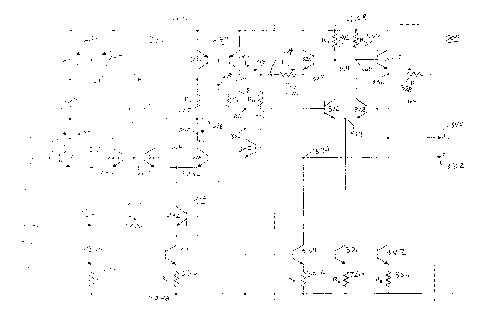
Referring to Figure 2 there is shown an embodiment of the present
invention. The circuit 200 operates as an integrated mixer (multiplier), filter, and
amplifier. The operation of the combined circuit may be better understood if the2 0 circuit is divided into four sections and each section explained separately. Each
section will first be discussed in general terms with a subsequent detailed
description.
379826 CA 02216~84 1997-09-29
The first section, within the dashed lines 202, is similar to the prior art
Gilbert four quadrant multiplier cell shown in Figure 1. The sum and difference
frequencies are coupled out of the first section, indicated by the dashed lines 202,
as current signals rather than as voltage signals as shown in Figure 1. The second
section, within the dashed lines 204, is a filter section which substantially limits the
unwanted high frequency signals from being coupled out of the first section and
subsequently amplified. The currents generated in the first section, indicated by
the dashed lines 202, are coupled to the second section, indicated by the dashedlines 204, which includes two resistors and a capacitor. The third section, within
0 the dashed lines 206, includes current transfer circuill~ that couples the filtered
baseband signal ~;ullcul~ to a shunt-shunt feedback structure that produces overall
voltage amplification. In the fourth section, within the dashed lines 208, the
baseband ~;ullcull~ flow through feedback resistors to generate the required voltage
swing. The voltage swing therefore only occurs at the IF+ outputs.
Referring now to the circuit in the first section, indicated by the dashed
lines 202, the circuit generally includes a circuit known as a transistor tree circuit
and includes the upper circuit 210 which includes the pair of differential amplifiers
212 and 214 and the lower circuit 218 which includes the dirrclclllial amplifier220. Each of the dirr~rclllial amplifiers 212, 214, and 220 include first and second
2 o NPN transistors; 222 and 224, 226 and 228, and 230 and 232, respectively. The
emitter electrodes of the transistors 222 and 224 are connected together and form
the common junction 234. The emitter electrodes of the transistors 226 and 228
379826 CA 02216~84 1997-09-29
are connected together and form the common junction 236. The common junction
234 is connected to the collector electrode of the transistor 230 and the commonjunction 236 is connected to the collector electrode of the transistor 232. The
collector electrodes of the transistors 222 and 226 are interconnected and form the
common junction 238. The collector electrodes of the transistors 224 and 228 areinterconnected and form the common junction 240.
The emitter electrodes of the transistors 230 and 232 are connected via the
resistor RIN 242 and to the collector electrodes of the NPN transistors 244 and 246,
respectively. The emitter electrodes of the transistors 244 and 246 are connected to
1 o the common ground line 248 via the bias resistors RB 250 and 252. The base
electrodes of the transistors 244 and 246 are connected to the source of voltage VB
254. The base electrodes of the transistors 230 and 232 are connected to the input
tçrmin~l~ 256 and 258 of the lower input port 260.
The base electrodes of the transistors 222 and 228 are interconnected and
form the common junction 261. The base electrodes of the transistors 224 and 226are interconnected and form the common junction 262. The common junctions
261 and 262 are connected to the input tçrmin~l~ 264 and 266, respectively. The
input termin~ls 264 and 266 form the upper input port 268.
Referring now to the circuit in the second section, indicated by dashed lines
2 o 204, the circuit is a filter circuit and includes the two resistors RS, 270 and 272, and
the capacitor Cs 274. One electrode of the resistor 270 is conn~cte~ to an electrode
of the capacitor Cs 274 and to the common junction 238 making one connection to
379826 CA 02216~84 1997-09-29
the circuit in the first section, indicted by the dashed lines 202. One electrode of
the resistor 272 is connected to the other electrode of the capacitor Cs 274 and to
the common junction 240 making a second connection to the circuit in the first
section, indicated by the dashed lines 202.
The common junction 276 is defined by the interconnection of an electrode
of the resistor Rs 270, an electrode of the capacitor Cs 274, and a connection to the
common junction 238. The common junction 278 is defined by the
interconnection of an electrode of the resistor Rs 272, an electrode of the capacitor
Cs 274, and a connection to the common junction 240.
1 o Referring now to the circuit in the third section indicated by dashed lines
206, the circuit generally includes current transfer Ch~;Uill~ including the first
current mirror 280, the second current mirror 282, and the bias level setting circuit
284 to set the bias level of the current mirrors 280 and 282. The first current
mirror 280 includes the two PNP transistors 286 and 288 and the second current
1 5 mirror 282 includes the two PNP transistors 290 and 292. The emitter electrodes
of the transistors 286, 288, 290, and 292 are connected to the positive voltage
supply line 294. The base electrodes of the transistors 286 and 288 are
interconnected and form the common junction 296. The common junction 296 is
connected to the collector electrode of transistor 286 at the common junction 297.
2 o The base electrodes of the transistors 290 and 292 are interconnected and form the
common junction 298. The common junction 298 is connected to the collector
electrode of transistor 290 at the common junction 300.
--10 -
379826 CA 02216~84 1997-09-29
The bias level setting circuit 284 includes the NPN transistor 302 with its
base electrode connected to its collector electrode forming the common junction
304 which is connected to the common junction 306 which is formed by the
interconnection of an electrode of the resistor RM 308 and an electrode of the
resistor RM 310. The emitter electrode of the transistor 302 is connected to thecommon ground line 248. The other electrode of the resistor RM 308 is connected
to the collector electrode of the transistor 288 forming the common junction at 312.
The other electrode of the resistor RM 310 is connected to the collector electrode
of the transistor 292 forming the common junction at 314.
1 o The common junction 297 is connected to an electrode of the resistor RS
270 making a first connection with the circuit in the second section 204. The
common junction 300 is connected to an electrode of the resistor Rs 272 making asecond connection with the circuit in the second section 204.
Referring now to the circuit in the fourth section indicated by dashed lines
208, the circuit generally includes the current to voltage amplifier 314. The current
to voltage amplifier 314 is a shunt-shunt feedback structure that produces overall
voltage amplification. The current to voltage amplifier 314 includes the NPN
transistors 316 and 318 and the NPN transistors 320 and 322. The emitter
electrodes of the NPN transistors 316 and 318 are interconnected forming the
2 o common junction 319. The common junction 319 is connected to the collector
electrode of the NPN transistor 321. The base electrode of the transistor 316 isconnected to the common junction 324 which is connected to the common junction
379826 CA 02216~84 1997-09-29
314 making a first connection to the circuit in the third section indicated by the
dashed lines 206. The base electrode of the transistor 316 is also connected to an
electrode of the resistor RF 326. The other electrode of the resistor RF 326 is
connected to the emitter electrode of the transistor 320 forming the common
junction 327. The collector electrode of the transistor 320 is connected to the
supply voltage Vs line 294. The common junction 327 is connected to the
cornmon junction 330 which is connected to the output tçnnin~l IF 332 and to thecollector electrode of the NPN transistor 334. The base electrode of the transistor
318 is connected to the common junction 312 making a second connection to the
o circuit in the third section, indicated by the dashed lines 206. The base electrode of
the transistor 318 is also connected to an electrode of the resistor RF 328. Theother electrode of the resistor RF 328 is connected to the emitter electrode of the
transistor 322 forming the common junction 336. The collector electrode of the
transistor 322 is connected to the supply voltage, Vs, line 329. The common
junction 336 is connected to the common junction 338 which is connected to the
output terrnin~l IF+ 340 and to the collector electrode of the NPN transistor 342.
The base electrode of the transistor 320 is connected to the collector
electrode of the transistor 316 forming the common junction 344. The common
junction 344 is connected to an electrode of the resistor RG 346. The other
2 o electrode of the resistor RG 346 is connected to the supply voltage Vs line 294.
The base electrode of the transistor 322 is connected to the collector electrode of
the transistor 318 forming the common junction 348. The common junction 348 is
-12-
379826 CA 02216~84 1997-09-29
connected to an electrode of the resistor RG 350. The other electrode of the resistor
RG 350 is connected to the supply voltage Vs line 294.
The emitter electrode of the transistor 334 is connected to the ground line
248 via the resistor RG 352. The emitter electrode of the transistor 321 is
connected to the ground line 248 via the resistor RG 354. The emitter electrode of
the transistor 342 is connected to the ground line 248 via the resistor RG 356.
The operation of the circuit is as follows. Referring to Figure 1 the
operation of the circuit, known as a Gilbert multiplier cell, is well known in the art.
A key operation in communications systems is a process known as mixin~, which
1 0 is the deliberate combination of two input signals of dirrer~lll frequencies in a time-
varying or nonlinear device to produce an output signal that contains new
frequencies. An analog multiplier, such as the Gilbert multiplier cell, mixes byproducing an output that is the in~t~n1:~neous product of signals applied to its two
inputs (thus the term "multiplier"). Gilbert multiplier cells are commonly used in
1 5 communications receivers as demodulators which separate useful information from
carrier signals. The Gilbert multiplier cell is also known as a four-quadrant
multiplier whose output is the product of its two inputs regardless of their algebraic
signs. In Figure 1 there is a first signal input at the port 136 from a local oscillator
(not shown). The input signal at the LO port 136 from the local oscillator is
2 o indicated as the LO+ signal input at the input terminal 132 and the LO signal input
at the input terminal 134. The input signal at the RF port 162 is mdicated as the
RF+ signal input at the input termin~l 158 and the RF signal input at the input
379826 CA 02216~84 1997-09-29
terminal 160 and is input from an external source (not shown). The external source
could be from a cable (such as a cable TV system) or an antenna which receives abroadcast signal (which could also be a TV system) on a carrier which is typically
a higher frequency than the frequency of the local oscillator. As is known in the
communications art, the circuit in Figure 1 will demodulate (mix) the two sets of
signals to output a set of intermediate frequency signals, the IF+ signal at the output
terminal 142 and the IF signal at the output t~rmin~l 144. The relationships
between the signals are as follows:
VIF+ ~ VIF- = K* (VRF+ ~ VRF-) * (VLO+ ~ VLO-)~ where VIF+ represents the voltage
of the IF+ signal, VIF- represents the voltage of the IF signal, etc. and VRF+ and
VRF- represent the voltages of the signals which are out of phase by 180 degrees;
the intermediate frequency fiF includes the frequency which is the sum of
the input frequencies, (fRF + fLO), and the frequency which is the difference of the
input frequencies, (fRF - fLO), The desired baseband frequency is the differencefrequency (fRF ~ fLo)
From the above relationships, it is observed that the frequency fiF is a
function of the sum of the two input frequencies, (fRF + fLO) and the differencebetween the two input frequencies (fRF - fLO). The desired baseband frequency isthe difference between the two frequencies. This indicates that there is a necessity
2 o to remove from the overall signal any component of the signal other than the
difference frequency of the two input frequencies. In addition, because the output
signal at the output tcrmin~l~ 142 and 144 is a di~lelllial voltage signal is the
--14--
379826 CA 02216~84 1997-09-29
basis of one of the limitations of the basic Gilbert cell, that is, the inability to
achieve a large voltage swing for a given supply voltage.
Referring to Figure 2 an embodiment of the present invention is shown and
the physical structure has been described above in detail. The portion of the circuit
within the dashed lines 202 is basically a mixer analogous to the Gilbert multiplier
cell shown in Figure 1. Similar to the operation of the circuit shown in Figure 1,
the circuit within the dashed lines 204 has a first signal input at the port 268 from a
local oscillator (not shown). The signal input at the port 268 from the local
oscillator is indicated as the LO+ signal input at the input t~rmin~l 264 and the LO
signal input at the input tçrmin~l 266. There is a second RF signal input at the port
260 from an external source (not shown). As discussed above, the ç~t~rn~l sourcecould be from a tuner output from a cable TV or satellite feed. The signal input at
the port 260 from the external signal source is indicated as the RF+ signal input at
the input terminal 256 and the RF signal input at the input tçrrnin~l 258. The
1 5 circuit within the dashed lines 202 will demodulate (mix) the two sets of signals.
However, unlike the circuit shown in Figure 1, a set of output voltages is not taken
from the collector electrodes of the pertinent transistors making up the dirre~"~ial
amplifiers 212 and 214. Tn~tça-l a set of differential ~;wl~llls, IBB+ flowing into the
common junction 276 and IBB- flowing into the common junction 278 are coupled
2 o to the remainder of the circuit 200. The relationships between the ac signals are as
follows:
cc+ = -ICc-~ and
--15--
379826 CA 02216~84 1997-09-29
ICC+ = IBBsin 2p(fRF - fLo)t + isR(t),
where iBR(t) is the parasitic residue spectrum of frequencies from the mixing
process and includes an important power component having the frequency sum (fRF
+ fLO)-
The ~ ICC+ and ICC- flowing into the common junctions 276 and 278
are within the filter circuit defined by the dashed lines 204 which includes thematched resistors Rs 270 and 272 and the capacitor Cs 274. The filter circuit isdesigned as a low pass filter which will subst~nti~lly filter out the high frequency
sum (fRF + fLO) leaving only the frequency difference, which is the desired
1 0 baseband signal, in the currents ICC+ and ICC- The sizes of the matched resistors Rs
297 and 300 and the capacitor Cs 274 are selected depending upon the frequenciesfRF and fLO. The method of selection of the values of the resistors Rs and the
capacitor Cs is well known in the art and will not be discussed herein.
The ~ ,nl~ IBB+ and IBB- flow from the common junctions 297 and 300,
s respectively, which are within the circuit indicated by the dashed line 206. The
circuit within the dashed lines 206 functions as a current conditioning circuit and
conditions the currents IBB+ and IBB- The current mirror 280 mirrors the currentIBB+ from the common junction 297 and causes the mirror current, indicated by
IBB'+~ to flow in the collector electrode of the transistor 288 to the common junction
2 0 312. Theoretically, a current mirror such as 280 mirrors a current "exactly."
However, practically a current mirror, because of m~nuf~cturing parameters, etc.,
does not "exactly" mirror the current. Therefore, the current IBB'+ is denoted with a
379826 CA 02216~84 1997-09-29
prime indicating that it may differ from the current IBB+. It is to be understood that
it is int~qnded for the current from the collector of transistor 288 to mirror that at the
common junction 297. Similarly, the current mirror 282 mirrors the current IBB-
from the common junction 300 and causes the mirror current, indicated by IBB'-~ to
flow in the collector electrode of the transistor 292 to the common junction 314.
The circuit, indicated at 284, sets the bias of transistors 288 and 292. The circuit
284 includes the two matched transistors RM 308 and 306 and the NPN transistor
302 acting as a diode, thus having a voltage drop of approximately 0.7 volts.
The circuit within the dashed lines 208 is a current-to-voltage amplifier and
converts the ~;UllClll~i IBB'+ and IBB'- to voltages, amplifies them, and outputs them at
the output termin~li 340 and 332. The circuit within the dashed lines 208 has
negative feedb~ck with the matched resistors RF 326 and 328 serving as feedback
resistors to the transistors 320 and 322. It is noted that the currents within the
dashed line 208 are denoted as IBB~+ and IBB~-- It is the intention that the ~ len~s
denoted as IBB~+ and IBB"- be equal to the (;U11Cnt~ denoted as IBB~+ and IBB'-~however, the .;u,lcn~ may, in practice, be different because of manllf~ctllring
differences. Therefore, the different decign~tions are to indicate that the ~ lcn~
may be slightly dirr~clll. The transistors 334, 321, and 342 together with the
matched resistors RB 352, 354, and 356 provide the proper bias for the transistors
2 o 320, 316, 318, and 322. The output signals IF+ and IF of the circuit 200 appear at
the output termin~l~ 340 and 332, respectively.
379826 CA 02216~84 1997-09-29
The foregoing description of the preferred embodiment of the invention has
been presented for purposes of illustration and description. It is not intended to be
exhaustive or to limit the invention to the precise form disclosed. Obvious
modifications or variations are possible in light of the above te~çhing~. The
embodiment was chosen and described to provide the best illustration of the
principles of the invention and its practical application to thereby enable one of
ordinary skill in the art to utilize the invention in various embodiments and with
various modifications as are suited to the particular use contemplated. All suchmodifications and variations are within the scope of the invention as determined by
the appended claims when interpreted in accordance with the breadth to which they
are fairly, legally, and equitably entitled.
--18 -