Note: Descriptions are shown in the official language in which they were submitted.
CA 02216812 2005-03-31
76199-63
COLOR FILTER AND LIQUID CRYSTAL DISPLAY APPARATUS
BACKGROUND OF THE INVENTION
1. Field of the invention
The present invention relates to a liquid crystal display apparatus driven by
electric fields parallel to a base plate and a color filter for use in the
liquid crystal
display apparatus.
2. Description of the related art
As described in some detail later with reference to Fig. 2, conventional color
liquid crystal display apparatuses of, for example, twisted nematic TN
(twisted
nematic) mode and IPS (in-plane switching) mode (lateral electric field
method)
normally employ glass fibers or plastic beads as a spacer between a color
filter-side
base plate and an electrode base plate provided with thin film transistors
(TFTs) and
a plurality of scan electrodes, in order to maintain the thickness of the
liquid crystal
layer (cell gap). The spacer such as a plurality of plastic beads is provided
by spraying,
so that the arrangement of individual spacer elements is uncontrollable,
thercby causing
problems of deterioration of the display quality of a liquid crystal display
device due
to light scattering by the spacer elements present on pixels.
Liquid crystal display devices employing sprayed spacer elements, such as
plastic beads, also have the following further drawbacks. Since the spacer
elements
have spherical or rod-like shapes, the spacer elements form point-like or line
or like
contacts during the pressing of an assembly of base plates into a cell and,
therefore,
may well break an alignment layer or a transparent electrode in the device,
possibly
resulting in a display defect. Breakage of an alignment layer or a transparent
electrode
will also contaminate the liquid crystal and result in a voltage decrease.
Furthermore, a step of uniformly spraying spacer elements is required, or
high-precision control of particle size distribution of the spacer elements is
required.
Thus, it is difficult to provide a liquid crystal display devicelaving a
stable display
quality by a simple method.
1
CA 02216812 2005-03-31
76199-63
Particularly in IPS mode liquid crystal display
apparatuses, there is a need to maintain a cell gap with an
increased consistency, thereby requiring an increased number
of spacer spraying steps. The IPS mode liquid crystal
display apparatuses also suffer more remarkably from the
aforementioned problems in that for example, due to its
material, the alignment layer may be fragile and conspicuous
light scatter by the spacer may occur due to the increased
back light intensity.
To solve these problems, JP-A-63-82405,
JP-A-04-93924, and JP-A-07-318950 propose a spacer structure
wherein two or three colored layers are laminated. However,
in TN-type liquid crystal display apparatuses, in order to
prevent a short circuit between transparent electrodes in a
portion where the spacer contacts a counter base plate and
electrodes in the counter base plate, there is a need to
form an insulating film in an upper portion of the counter
base plate or the spacer or a need to restrict the position
where the spacer is formed or the size of the spacer,
thereby making production of a liquid crystal display
apparatus difficult.
SUMMARY OF THE INVENTION
Accordingly, the present invention seeks to
provide a color liquid crystal display apparatus that is
easy to produce and excellent in display quality with a high
contrast and a wide visual field angle.
Thus, the present invention provides a liquid
crystal display apparatus comprising:
(A) a color filter base plate having a transparent
substrate, a black matrix and a colored film of three
2
CA 02216812 2005-03-31
76199-63
primary colors provided on the transparent substrate in this
order;
(B) an electrode-carrying counter base plate
provided with electrodes for applying an electric field
parallel to the color filter base plate; and
(C) a liquid crystal filled in a cell gap between
the color filter base plate and the electrode-carrying
counter base plate arranged so that the black matrix and the
electrodes face each other,
wherein the colored film is formed on the black
matrix by patterning a resin, and acts as a spacer to make
the cell gap uniform.
The present invention also provides a color filter
for use in producing a liquid crystal display apparatus
together with a liquid crystal and an electrode-carrying
base plate provided with electrodes for applying an electric
field parallel to the color filter, which color filter
comprises:
a transparent substrate;
a black matrix formed on the transparent substrate
by patterning a light-shielding material, the black matrix
having openings; and
a colored film of three primary colors provided in
patterns separately for each color employed, wherein a
spacer is formed on the black matrix by patterning a resin.
BRIEF DESCRIPTION OF THE DRAWINGS
2a
CA 02216812 2003-05-06
76199-63
A preferred embodiment of the present invention
will be described in detail hereinafter with reference to
the accompanying drawings, _i.n which:
Fig. 1 is a schematic sectional view of a color
liquid crystal display apparatus according to an embodiment
of the present invention;
Fig. 2 is a sectional view of a conventional color
liquid crystal display apparatus; and
Fig. 3 is a schematic sectional view of a color
liquid crystal display apparatus according to another
embodime:nt of the present invention.
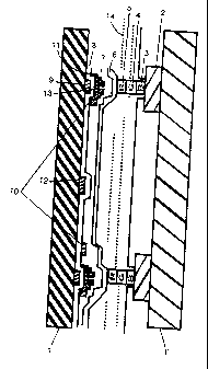
Referring firstly to Fig. 2, a known color filter
fc:>r use in a liquid crystal display apparatus comprises a
transparent substrate 1' carrying, on its upper surface, a
black matrix 2. Disposed above and spaced from the
transparent substrace 1' is an upper substrate 1, from a
lower surface of which project gate electrodes 9 and a
common electrode 12. An insulating film 8 covers a:rid is
profiled to be in face to face contac:t::: with the dow:riwardly
facing surface and gate and common electrodes 9 and 12.
Each of a drain electrode i{), a source electrode
11 and a thin film transistor 13 depends downwardly from the
insulating film 8. This arrangement of electrodes 9-12 is
designed to apply an electrode field parallel to the color
filter. A profiled protective film 7 covers and lies in
face to face contact with the insulaL_s..ng film 8 and drain
arid source electrodes 10 and 11. The protective film 7 is
in turn covered by an alignment layer 6. A gap therefore
exists between an upwardly facing black matrix 2 on the
transparent substrate 1' and the downwardly facing alignment
~?,
CA 02216812 2003-05-06
76199-63
layer 6 on the upper substrate 1. In this gap sits a liquid
crystal 14. In this known color filter, the gap iss
maintained by a plu.ral;ty of beads 35.
Referring now to Fig. 1, a.1 i.r4ui.d crystal display
apparatus embodying the invention has all of the components
described above with reference to Fig. 2, except that the
gap in which the liquid crystal 14 sits is maintained not by
beads, but by color layers 3, 4 and 5, being blue, green and
red layers, respectively, stacked one above the other. Fig.
3 illustrates the liquid crystal display apparatus that is
the same as that of Fig. 1, except that the gap in which the
liquid crystal 14 sits is maintained by a single layer 16,
in place of the layers 3, 4 and 5.
DETAILED DESCRIPTION OF THE PREFERRED EMBODIMENTS
More particularly, the color filter used in the
present invention has a transparent subsi:::rat.e, ar.id a black
matrix formed by patterning a light-shielding
3a
CA 02216812 1997-09-25
material. Openings in the black matrix are covered with pixels formed by
colored
layers provided in desired patterns separately for each color employed. The
number
and types of colors to be employed may be chosen at will. Spacer elements are
formed
on the black matrix by patterning a resin. The color filter may further have
an overcoat
layer that is formed on the colored layers if necessary. The color filter is
used in a
color liquid crystal display apparatus driven by electric fields parallel to
the transparent
base plate (lateral electric fields). This type of color liquid crystal
display apparatus
does not require a common electrode provided on the side of the color filter
base plate,
unlike a normal TN mode color liquid crystal display apparatus. Therefore,
even
though the spacer formed on the color filter base plate contacts the counter
base plate,
there is no short circuit between the common electrode and pixel electrodes or
wiring
on the counter base plate. The restrictions on the size of the spacer are
therefore
reduced. Further, the need to provide an insulating film on the side of the
counter base
plate is eliminated. Thereby, production of the liquid crystal display
apparatus is
facilitated because the number of man hours is reduced and the processing
precision
is improved. Furthermore, for the lateral electric field liquid crystal
display
apparatuses, which require control of a cell gap between the base plates with
an
increased precision, the color filter having a spacer formed by patterning is
especially
suitable because spacer elements having consistent heights and sizes can be
uniformly
arranged in the base plate, thereby making it possible to provide a uniform
cell gap.
The resin layer forming the spacer may be a single layer, or a plurality of
laminated
layers if a single layer fails to provide a sufficient height.
The resin layer forming the spacer according to the present invention is
preferably formed of a material capable of bearing loads during production of
a liquid
crystal panel. Preferable examples of such a material are photosensitive or
non-
photosensitive materials such as polyimide-based resin, epoxy-based resin,
acrylic
resin, urethane-based resin, polyester-based resin and polyolefin-based resin.
There are several types of photosensitive resin, for example,
photodegradable resin, photo crosslinking resin and photopolymerizing resin.
Particularly preferred in a color filter embodying the present invention are,
for example,
photosensitive compositions such as photosensitive polyamic acid compositions,
4
CA 02216812 2003-05-06
76199-63
containing monomers, oligomers or polymers having ethylene unsaturated bonds
and
an initiator that generates radicals in response to ultraviolet rays.
As for the non-photosensitive resin, resins enabling image or pattern
development are preferably used. The non-photosensitive resin used in the
present
invention preferably has resistance to heat applied during the process for
producing the
liquid crystal display apparatus and also preferably has resistance to any
organic
solvent used during the process for producing the liquid crystal display
apparatus.
Polyimide-based resin is more preferably used, due to its high resistance to
heat and
organic solvents and its excellent mechanical properties for use as a spacer.
The polvimide resin used to prepare a spacer in a liquid crystal display
apparatus embodying the present irlverrtion may be a resin obtained by
applying to a
substrate solution of a polyimide precursor and subjecting it to heat
treatment, whereby
a polymer (polyimide, polyamideimide) having imide ririgs or other cyclic
structures
is produced. The polyimide precursor may be a poly (amic acid) containing a
structure
1s unit (I) as a main component (ie no other structure unit is present in a
greater molar
proportion), which structure unit (1) has the formula
-[CO-RI-CONH-R4-NH]-
1 (1)
(COOH)n
The polyimide-based resin may have bonds other than imide bonds, such as
amide bonds, sulfone bonds, ether bonds and carbonyl bonds, without causing
any
significant drawback.
In the general formula (1), n is 1-2, and Rr is a trivalent or tetravalent
organic group having at least two carbon atoms. For improved heat resistance,
Ri is
preferably a trivalent or tetravalent group having a cyclic rrydrocarbon, an
aromatic ring
or an aromatic heterocyclic ring in which the number of carbon atoms is 6 to
30.
Examples of Rt are a phenyl group, biphenyl group, terphenyl group,
naphthalene
group, perylene group, diphenyl ether group, diphenyl sulfone group, diphenyl
propane
group, benzophenone group, biphenyl trifluoropropane group, cyclobutyl group
and
a cyclopentyl group. However, Rr is not limited to these groups. R2 is a
bivalent
organic group having at least two carbon atoms. For improved heat resistance,
R_ is
CA 02216812 1997-09-25
preferably a bivalent group having a cyclic hydrocarbon, an aromatic ring or
an
aromatic heterocyclic ring in which the number of carbon atoms is 6 to 30.
Examples
of R2 may be a phenyl group, biphenyl group, terphenyl group, naphthalene
group,
perylene group, diphenyl ether group, diphenyl sulfone group, diphenyl propane
group,
benzophenone group, biphenyl trifluoropropane group, diphenyl methane group
and
a cyclohexyl methane group. However, R2 is not limited to these groups. In the
polymer containing as a main component the structure unit represented by
general
formula (1), each of R1 and R2 may be formed by one of these groups or may be
a
copolymer formed by two or more of these groups. In order to increase the
adhesion
to a substrate, it is possible to copolymerize with, for example, bis-(3-
aminopropyl)tetramethyl disiloxane having a siloxane structure, as a diamine
component in an amount within a range that will not reduce the heat
resistance. It is
also possible to add, as an amino terminal sealer, an anhydride such as maleic
anhydride, in an amount in accordance with the concentration of terminals
after
polymerization of a polyimide precursor, and allow it to react.
The mechanical properties of the polyimide film become better with
increasing molecular weight. Therefore, it is desirable that a polyimide
precursor have
a large molecular weight. However, if a polyimide precursor is subjected to
wet
etching for patterning, an excessively large molecular weight of the polyimide
precursor results in an inconveniently long development time. Therefore, it is
normally
preferred that the degree of polymerization be within a range of 5 to 1000.
The resin that forms the spacer may contain a coloring agent if necessary.
As a coloring agent, an organic pigment, an inorganic pigment or a dye may be
used.
It is further possible to add various additives, such as an ultraviolet
absorbing agent or
a dispersion agent, a leveling agent. If the spacer needs to have a light-
shielding
characteristic, it is possible to use a light shielding agent, such as carbon
black, powder
of a metal oxide such as titanium oxide or iron tetroxide, metal sulfide
powder, metal
powder, and further a mixture of pigments of, for example, red, blue and green
color.
Among these, carbon black has an excellent light shielding characteristic and
therefore
is particularly preferred. If the spacer needs to have an insulating
characteristic as well
as a light shielding characteristic, it is possible to use carbon black whose
surfaces are
6
CA 02216812 1997-09-25
coated with fine particles of an insulating inorganic compound such as
titanium oxide
or iron oxide.
In a liquid crystal display apparatus embodying the present invention, it is
preferable that the spacer be formed in non-display areas inside and outside
the display
screen area. In this manner, the interval between the two base plates of the
liquid
crystal display device can be more consistently maintained within the display
apparatus
screen.
The spacer, formed by patterning the resin layer according to the present
invention, is preferably formed by laminating a colored layer that covers the
open
io portions of the matrix, more preferably, by laminating layers of three
primary colors.
By forming the spacer by laminating a colored layer, the spacer can be formed
simultaneously with production of a color filter without increasing the number
of
processing steps. Furthermore, by lamination of three primary color layers, it
becomes
easy to provide a sufficient cell gap without increasing the film thickness of
each
is colored layer. If lamination of three primary color layers does not provide
a sufficient
height, an additional resin layer may be laminated.
A liquid crystal display apparatus according to the present invention has
light shielding areas arranged between individual pixels, called a "black
matrix". With
the black matrix provided, the color filter improves the contrast of the
liquid crystal
20 display apparatus.
As a black matrix, thin metal films (having a thickness of about 0.1-0.2,um)
of, eg Cr, Al or Ni or resin black matrixes wherein a light shielding agent is
dispersed
in a resin are normally employed. In the present invention, it is more
preferable to use
a resin black matrix formed by dispersing a black pigment in a polyimide film.
This
25 is because such a resin black matrix has a low reflectivity and a good heat
resistance
and a good solvent resistance and, moreover, has a low relative dielectric
constant so
that it causes less disturbance to the lateral electric fields. Furthermore,
it is possible
to provide the resin black matrix with a capacity for orienting liquid crystal
by rubbing
as performed on the pixels.
30 Furthermore, resin black matrixes are easy to increase in thickness
compared
with metal thin films, so that it is easier to form a spacer that provides a
sufficient cell
7
CA 02216812 1997-09-25
gap by forming a spacer on a resin black matrix.
Examples of the light shielding agent usable in the black matrix are carbon
black and a powder of a metal oxide such as titanium oxide or iron tetroxide,
metal
sulfide powder, metal powder, and also a mixture of pigments of, for example,
red,
blue or green color. Among these, carbon black has an excellent light
shielding
characteristic and therefore is particularly preferred. Since carbon black
having small
particle diameters and therefore good dispersibility normally exhibits a
brownish color
tone, it is preferred to mix such carbon black with a pigment of complementary
color
to render it black.
If the black matrix is formed of a polyimide resin, it is normally preferred
to use, as a black paste solvent, an amide-family polar solvent such as N-
methyl-2-
pyrrolidone, N,N-dimehtylacetoamide or N,N-dimethylformamide or a lactone-
family
polar solvent such as y -butylolactone.
The method for dispersing carbon black or a light shielding agent such as
a pigment of complementary color to the carbon black may be, for example, a
method
wherein after a light shielding agent and, for example, a dispersing agent are
mixed into
a polyamide precursor solvent, they are dispersed in a dispersing machine such
as a
three-roll machine, a sand grinder or a ball mill. It is also possible to add
various
additives for providing improvements in the dispersion, application
characteristic and
leveling characteristic of the carbon black.
The resin black matrix may be produced by applying a black paste on the
transparent substrate, drying the paste and then patterning. The black paste
may
preferably be applied by, for example, a dip method, a roll coater method, a
spinner
method, a die coating method or a method using a wire bar. After being
applied, the
paste may be heated and dried (semi-cured) using an oven or a hot plate. The
semi-
cure conditions vary depending on the resin and solvent used, and the amount
of paste
applied. It is normally preferred to heat the paste at 60-200 C for 1-60
minutes.
If the resin of the black paste coating thus formed is a non-photosensitive
resin, a positive photoresist coating is formed thereon before exposure and
development. If the resin is a photosensitive resin, the black paste coating
is exposed
and developed immediately or after an oxygen blocking film is formed. Then,
after the
8
CA 02216812 1997-09-25
positive photoresist or the oxygen blocking film (if necessary) is removed,
the
developed coating is subjected to heating and drying (main cure). In a case
where a
polyimide-based resin is obtained from a precursor, the main cure conditions
slightly
vary depending on the amount of paste applied. Normally, the coating is heated
at 200-
300 C for 1-60 minutes. Through these processes, a black matrix is formed on a
substrate.
It is also possible to form a resin black matrix by a so-called transfer
method. In this method, a transfer film wherein a black layer provided with a
photosensitive component is formed on a base is prepared beforehand, and the
film is
laid on a substrate (heated and pressurized if necessary) for exposure and
development.
After that, the base is peeled leaving a resin black matrix formed on the
substrate.
The film thickness of the resin black matrix is preferably 0.5-2.0 ,um and,
more preferably, 0.8-1.5,um. If the film thickness of the resin black matrix
is less than
0.5,um, it becomes difficult to reliably provide a sufficient cell gap and,
further, the
light shielding characteristic becomes insufficient. If the film thickness is
greater than
2.0,um, it becomes likely that the flatness of the liquid crystal display
apparatus will
be sacrificed, resulting in a stepped or irregular surface, although a
sufficient cell gap
may be reliably provided.
The light shielding characteristic of the resin black matrix may be
represented by an OD value (common logarithm of the inverse of transmittance).
To
improve display quality of the liquid crystal display apparatus, the OD value
is
preferably 2.5 or higher and, more preferably, 3.0 or higher. The upper limit
of the OD
value should be determined based on the relationship with the aforementioned
preferable range of the film thickness of the resin black matrix.
The reflectivity of the resin black matrix is preferably 2% or lower in terms
of the reflectivity (Y value) corrected by a visibility factor within a visual
light range
of 400-700 nm and, more preferably, 1% or lower.
Each opening in the black matrix is normally 20-200,um x 20-300,um. The
colored layer is formed such that such open portions in the black matrix are
covered.
The colored layer in a liquid crystal display apparatus embodying the
present invention is a layer formed by a film having a capacity for
transmitting any
9
CA 02216812 1997-09-25
selected color of light. The colored layer may be formed of any material.
Normally,
a liquid crystal display apparatus according to the present invention includes
at least
three layers of three primary colors, that is, red (R), green (G) and blue
(B), or cyan
(C), magenta (M) and yellow (Y), and each pixel is provided with one of the
three
colored layers. Examples of specific materials for the colored layer are a
polyimide
film wherein a coloring agent, a pigment or a dye is dispersed, a PVA
(polyvinyl
alcohol) treated with staining or a Si02 film whose thickness has been
controlled so
that only selected light is transmitted. A polyimide film wherein a pigment is
dispersed
is more preferable because the polyimide film makes it possible to form a
colored layer
through a process comparable with or easier than the processes required for
other
materials and, moreover, the polyimide film is better in heat resistance,
light resistance
and chemical resistance. Furthermore, employment of the polyimide film is
preferred
for improved mechanical properties in a case where the colored layer is used
as a
spacer.
The relative dielectric constant of the colored layer according to the present
invention is preferably less than 4.5 and, more preferably, 3.6 or less. To
effectively
apply electric fields to the liquid crystal in a direction parallel to the
base plate, it is
desirable that the relative dielectric constant of the color filter-
constituting materials
be less than either the shorter axis component or the longer axis component of
the
relative dielectric constant of the liquid crystal, more preferably, 1/2 or
less. This is
because with an increase in the relative dielectric constant of the color
filter-
constituting materials, the deviation of the direction of an electric field
from the
direction parallel to the base plate at the interface between the liquid
crystal and the
color filter increases, so that the effective electric field decreases and,
therefore, the
liquid crystal switching efficiency decreases. For a color filter without an
overcoat, the
colored layer is preferably formed of a material having a reduced relative
dielectric
constant because then the colored layer contacts the liquid crystal directly
or with an
alignment layer provided therebetween. For a color filter having an overcoat,
it is also
preferred that the colored layer be formed of a material having a reduced
relative
dielectric constant so as to achieve a reduction of the relative dielectric
constant of the
entire color filter.
CA 02216812 1997-09-25
The maximum component of the relative dielectric constant of the liquid
crystal used in liquid crystal display apparatuses driven by thin film
transistors is
normally about 8-12 or at least 4.5. Therefore, the relative dielectric
constant of the
colored layer is preferably less than 4.5 and, more preferably, 3.6 or less.
The relative
dielectric constant herein refers to values measured at 20 C within a
frequency of 100
Hz-100 kHz.
The colored layer according to the present invention is more preferably a
film provided with a capacity for orienting liquid crystal molecules in
contact therewith
by an orientation method such as rubbing, hereinafter referred to as an
"alignment
layer". Thereby, it becomes possible to omit a step of separately applying an
alignment
layer on a color filter during production of a liquid crystal display panel.
It is desirable that the colored layer according to the present invention have
a surface that is smooth as much as possible. More specifically, the colored
layer
surface desirably has an Ra value of 0.010 m or lower, the Ra value being a
measured
value indicating a surface roughness. This level of surface roughness will
prevent
occurrence of an orientation failure during rubbing and therefore prevent a
display
failure caused by an orientation failure.
Pigments used in the present invention are not particularly limited.
Preferred are pigments excellent in light resistance, heat resistance and
chemical
resistance. Specific examples of representative pigments are cited below with
reference
to their Color Index (CI) numbers. Examples of yellow pigments are CI Pigment
Yellow 20, 24, 83, 86, 93, 94, 109, 110, 117, 125, 137, 138, 139, 147, 148,
153, 154,
166 and 173. Examples of orange pigments are CI Pigment Orange 13, 31, 36, 38,
40,
42, 43, 51, 55, 59, 61, 64 and 65. Examples of red pigments are CI Pigment Red
9, 97,
122, 123, 144, 149, 166, 168, 177, 180, 192, 215, 216 and 224. Examples of
purple
pigments are CI Pigment Violet 19, 23, 29, 32, 33, 36, 37 and 38. Examples of
blue
pigments are CI Pigment Blue 15 (eg. 15:3, 15:4 and 15:6), 21, 22, 60 and 64.
Examples of green pigments are CI Pigment Green 7, 10, 36 and 47. An example
of
a black pigment is CI Pigment Black 7. It is also possible to use pigments
subjected
to surface treatment such as rosin treatment, acidic group treatment and basic
group
treatment if desired.
11
CA 02216812 1997-09-25
A colored layer may be formed by applying to a substrate on which a black
matrix has been formed, and then drying and patterning. The method for
dispersing or
dissolving a coloring agent such as a pigment may be, for example, a method
wherein
after a resin and a coloring agent are mixed into a solvent, the resin and
coloring agent
are dispersed in a dispersing machine such as a three-roll machine, a sand
grinder or
a ball mill.
The colored paste is preferably applied, as in application of a black paste,
for example, by a dip method, a roll coater method, a spinner method, a die
coating
method or a method using a wire bar. After being applied, the paste may be
heated and
dried (semi-cured) using an oven or a hot plate. The semi-cure conditions vary
depending on the resin and solvent used, and the amount of paste applied. It
is
normally preferred to heat the paste at 60-200 C for 1-60 minutes.
If the resin of the colored paste coating thus formed is a non-photosensitive
resin, a positive photoresist coating is formed thereon before exposure and
development. If the resin is a photosensitive resin, the colored paste coating
is exposed
and developed immediately or after an oxygen blocking film is formed. Then,
after the
positive photoresist or the oxygen blocking film (if necessary) is removed,
the
developed coating is subjected to heating and drying (main cure). The main
cure
conditions vary depending on the resin. However, in a case where a polyimide-
based
resin is obtained from a precursor, the coating is normally heated at 200-300
C for 1-
60 minutes. Through these processes, a patterned colored layer is formed on
the
substrate carrying the black matrix formed thereon.
After a first color layer is formed over the entire surface of the substrate
carrying the black matrix, unnecessary portions may be removed by
photolithography,
thereby forming a desired pattern of the first color layer. The second and
third color
layers may be formed by similar procedures into desired color layer patterns.
In the color filter of the present invention, it is possible to provide an
overcoat film on the colored layer if desired. The overcoat film herein is a
film formed
for protection of the colored layers or the flattening of the color filter
surface. In an IPS
mode liquid crystal display apparatus, the overcoat film will achieve an
advantage of
shielding an electrically conductive material, such as a metal black matrix,
so as to
12
CA 02216812 1997-09-25
effectively apply lateral electric fields to the liquid crystal. As in the
colored layers,
the overcoat film is more preferably a film provided with a capacity for
orienting liquid
crystal molecules in contact therewith by an orientation method such as
rubbing.
Thereby, it becomes possible to produce a liquid crystal display apparatus
without a
need to separately form an alignment layer on the color filter, thereby
reducing the
number of production processes. Further, in the color filter of the present
invention,
the overcoat film will be effective in improving the physical properties of
the spacer.
Moreover, it will become possible to adjust the height of the spacer by
rendering the
overcoat film thickness over the display area less than the overcoat film
thickness over
the spacer.
Specific examples of the overcoat film may be inorganic films of, for
example, Si02, and organic films such as epoxy films, acrylic epoxy films,
acrylic
films, siloxane polymer films, polyimide films, silicon-containing polyimide
films and
polyimide siloxane films. Preferred are polyimide-based high molecular weight
films,
such as polyimide films, silicon-containing polyimide films and polyimide
siloxane
films, due to their excellent flatness, applicability and heat resistance and,
furthermore,
their superiority over the other films in their capacity for restricting the
orientation of
the liquid crystal.
The polyimide siloxane film according to the present invention may be a
film produced by heat-treating a polyimide siloxane precursor coating. The
polyimide
siloxane precursor coating can be produced by various procedures. In a
representative
procedure, a silicon compound having in its molecule at least one primary
amino group
or at least one secondary or higher alkoxide group is reacted with a
tetracarboxylic
dianhydride in an organic solvent, thereby producing a precursor coating. The
reaction
product may further be hydrolyzed and condensed to produce a precursor
coating.
The overcoat film in a color filter embodying the present invention
preferably has a surface that is smooth as much as possible. More
specifically, the
overcoat film surface desirably has an Ra value of 0.01,um or lower, the Ra
value being
a measured value indicating a surface roughness. This level of surface
roughness will
prevent occurrence of an orientation failure during rubbing and therefore
prevent a
display failure caused by an orientation failure.
13
CA 02216812 1997-09-25
The relative dielectric constant of the overcoat film in the present invention
is preferably less than 4.5 and, more preferably, 3.6 or less, for the same
reason as
stated above in conjunction with the colored layer. In particular, it is
preferred that the
overcoat film that contacts with liquid crystal directly or with an alignment
layer
provided therebetween be formed by a material having a further reduced
relative
dielectric constant. The relative dielectric constant herein refers to a value
measured
at 20 C with a frequency of 100 Hz-100 kHz.
The overcoat may preferably be applied, as in application of a black paste,
by, for example, a dip method, a roll coater method, a spinner method, a die
coating
method or a method using a wire bar. After application, heating and drying
(semi-cure)
may be performed using an oven or a hot plate. The semi-cure conditions vary
depending on the resin and solvent used, and the amount applied. It is
normally
preferred to heat it at 60-200 C for 1-60 minutes.
The thus-formed overcoat film may then heated and dried (main-cured).
The main cure conditions vary depending on the resin. If a polyimide-based
resin is
obtained from a precursor, the overcoat film is normally heated at 200-300 c
for 1-60
minutes. Through these processes, the overcoat film is formed.
The orientation treatment in the present invention may be performed by any
method as long as the method provides the colored layers or the overcoat film
with
capacity for orienting liquid crystal in contact therewith. Specific examples
of such
method are a rubbing method, an oblique vapor deposition method and a grating
method. Among these, a rubbing method is more preferably used because the
method
can be performed by a relatively simple apparatus so as to provide a high
productivity
on an industrial scale, and can provide a high orientating capacity.
The rubbing method used in preparing a color filter embodying the present
invention is a method wherein a cloth (for example) is rubbed in a single
direction
against a film, that is, the object of orientation treatment. The liquid
crystal molecules
that contact with the rub-treated film are oriented in the rubbing direction.
The material
to be rubbed against the film varies depending on the hardness of the film to
be treated.
For a polyimide film, a cotton cloth or a rayon cloth having a staple length
of 2-3 mm
is normally used.
14
CA 02216812 1997-09-25
The color filter of the present invention preferably has an electrically
conductive transparent film provided on the reverse face of a base plate. The
reverse
face of the base plate is that face opposite from the face that contacts with
the liquid
crystal when a liquid crystal display apparatus is assembled. With the
electrically
conductive transparent film provided on the reverse face of the base plate,
the charging
of the base plate can be prevented. Charges in the base plate can cause
deficiencies or
problems such as a defective conveyance of the base plate during production
processing
steps, deposition of contaminants due to static electricity and breakage of
thin film
transistors in the counter base plate. Furthermore, an electric field caused
by static
electricity may disturb the orientation of the liquid crystal inside the cell
and thereby
cause a display defect. Examples of the electrically conductive transparent
film
employed in the present invention are an electrically conductive transparent
film
formed mainly from a metal or a metal oxide, or an electrically conductive
transparent
film formed mainly from an alloy of a combination of several kinds of metals
and metal
oxides.
Specific examples of a main component of the electrically conductive
transparent film are metals and metal oxides such as Al, Mo, Cr, Ta, Cu, W,
Ti, Au, Te,
TeSe, In, Ge, Th, Dy, Gd, ZnS, TbFe, DyFe, Gd, Si02, SiO, SiC, S15N4, AIN,
ITO,
In203, Sn02, ZnO, ZnS, CaS, SrS, Ta205, W03, Y203, SrTiO3, BaTiO3, PbTiO3,
A1203, NiCr, TaSiO2 and TiCSiO3. Practically, alloys of combinations of
several
species of these metals and metal oxides may be used. Among these, ITO is
preferably
used because it does not sacrifice the transparency and is excellent in
electric
conductivity.
The specific resistance of the electrically conductive transparent film is
normally 2 k Q =cm or less and, preferably, 600 Q =cm and, more preferably,
300 SZ
=cm. If the specific resistance of the electrically conductive transparent
film is
excessively great, a sufficient charge preventing effect may not be achieved.
The transmittance of the electrically conductive transparent film according
to the present invention is preferably 96% or higher and, more preferably, 98%
or
higher. If the transmittance of the electrically conductive transparent film
is lower, the
transmittance of the color filter may become inconveniently low and the
contrast also
CA 02216812 1997-09-25
decreases to an undesirable level.
The thickness of the electrically conductive transparent film in a color
filter
embodying the present invention is preferably 10 nm to 100 nm and, more
preferably,
20 nm to 50 nm. If the thickness of the electrically conductive transparent
film is
excessively small, a sufficient charge preventing effect may not be achieved.
If the
film thickness is excessively great, the transmittance may decrease to an
undesired
level.
An example of the method for forming a spacer through lamination of
colored layers in a color filter according to the present invention will be
described
below.
After a first color layer is formed over the entire surface of the base plate
carrying the resin black matrix formed thereon, unnecessary portions are
removed by
photolithography, thereby forming a desired pattern of the first color layer.
Portions
of the colored layer that cover openings in the resin black matrix and that
form spacer
1s elements through lamination of colored layers are left on the base plate.
The second
and third color layers are formed and left on the base plate by similar
procedures, so
that the openings in the resin black matrix are covered with one of the three
colored
layers and the three layers are left to provide spacer elements. The colored
layers over
the openings and the colored layers forming the spacer elements may be
continuous or
separate from each other.
The thickness of the three primary color layers is not particularly limited.
However, the thickness of each layer is preferably 1-3 ,um, so that the total
thickness
of the three layers amounts to 3-9,um. If the total film thickness is less
than 3,um, a
sufficiently large cell gap may not be obtained. If the total film thickness
exceeds 9
um, it may become difficult to uniformly apply the colored layers.
If the color filter of the present invention is used to maintain a cell gap in
a
case, for example, where R, G and B are selected as the three colors, the cell
gap for
R in the liquid crystal display apparatus corresponds to the film thickness of
G + B +
Bk (resin black matrix), and the cell gap for G corresponds to the film
thickness of B
+ R + Bk, and the cell gap for B corresponds to a film thickness of R + G +
Bk. If the
dispersibility of the coloring agents in the pastes for forming the colored
layers is
16
CA 02216812 1997-09-25
improved or if the leveling characteristic is improved for the purpose of
uniform
application, the height of the spacer formed by lamination of the three
primary color
layers becomes less than the total film thickness of the three color layers
over pixels.
That is, the cell gap for R becomes less than the total thickness of G + B +
Bk, and,
likewise, the cell gap for G becomes less than the total thickness of B + R +
Bk, and
the cell gap for B becomes less than the total thickness of R + B + Bk.
The spacer formed by lamination of the three primary color layers according
to the present invention is formed on the resin black matrix as described
above. The
areas and locations of spacer elements on the black matrix are strongly
dependent on
the structure of the active matrix base plate that faces the color filter when
a liquid
crystal display device is produced. If no such restriction is imposed by the
counter
electrode base plate, the areas and locations of the spacer elements are not
particularly
limited. However, considering the pixel size, the area of each spacer element
is
preferably 10 m2 to 1000 ,um2. If the area of each spacer element is less
than 10 ,um2,
it may become difficult to form a minute and precise pattern and laminate. If
it is
greater than 1000,um2, it may become difficult to arrange the spacer elements
precisely
on the black matrix, depending on the configuration of the spacer elements.
The liquid crystal display apparatus of the present invention has an excellent
feature namely that of a wide view field angle, because it is driven by
lateral electric
fields. Moreover, since no spacer exists in the pixels, deterioration of the
display
quality caused by light leakage through the spacer or light scatter thereby
are
eliminated. Furthermore, since the liquid crystal display apparatus has fixed
spacer
elements that are formed and regularly arranged by patterning the resin
layers, the cell
gap becomes uniform, thereby improving the display quality. Thus, the present
invention makes it easy to provide a TFT liquid crystal display apparatus with
a wide
view field angle and an improved display quality. Further, since thin film
transistors
(TFTs) are provided in the electrode-carrying base plate, it becomes possible
to
produce a TFT liquid crystal display apparatus further improved in display
quality.
EXAMPLE 1
[Production of Black Matrix]
17
CA 02216812 1997-09-25
3,3' ,4,4' -Biphenyl tetracarboxylic dianhydride, 4,4' -diaminodiphenyl ether
and bis(3-aminopropyl)tetramethyl disiloxane were reacted in a solvent of N-
methyl-2-
pyrrolidone, thereby obtaining a polyimide precursor (polyamic acid) solution.
A carbon black mill base having the following composition was dispersed
at 7000 rpm for 30 minutes using a homogenizer. Glass beads were filtered out,
thereby preparing a black paste.
<Carbon mill base>
Carbon black (MA100 by Mitsubishi
Kasei Kabushiki Gaisha) 4.6 parts
Polyimide precursor solution 24.0 parts
N-methyl pyrrolidone 61.4 parts
Glass beads 90.0 parts
The black paste was applied to a no-alkali glass (OA-2 by Nippon Denki
Glass Kabushiki Gaisha) substrate having a size of 300 x 350 mm using a
spinner. The
applied paste was semi-cured at 135 C in an oven for 20 minutes. A positive
resist
(Shipley "Microposit" RC100 30cp) was then applied using a spinner, after
which the
resist was dried at 90 C for 10 minutes. The resist film thickness was
1.5,um. The
positive resist was then exposed through a photomask using an exposure
apparatus
PLA-501F by Canon Kabushiki Gaisha.
The substrate was dipped in a developer aqueous solution at 23 C. The
aqueous solution contained 2% by weight of tetramethylammonium hydroxide. The
substrate was oscillated in such a manner that the substrate reciprocated over
a distance
of 10 cm once in every five seconds, thereby simultaneously performing
development
of the positive resist and the etching of the polyimide precursor. The
development time
was 60 seconds. After that, the positive resist was peeled using methyl
cellosolve
acetate. The substrate was then cured at 300 C for 30 minutes, thereby
obtaining a
resin black matrix. A spacer pattern was simultaneously formed outside the
screen
area. The film thickness of the resin black matrix was 0.90,um, and the OD
value
thereof was 3Ø The reflectivity (Y value) at the interface between the resin
black
matrix and the glass substrate was 1.2%.
18
CA 02216812 2003-05-06
76199-63
[Production of Colored Layers]
As red, green and blue pigments, a dianthraquinone-based pigment indicated
by Color Index No. 65300 Pigment Red 177, a phthalocyanine green-based pigment
indicated by Color Index No. 74265 Pigment Green 36, and a phthalocyanine blue-
based pigment indicated by Color Index No. 74160 Pigment Blue 15-4 were
prepared.
These pigments were separately mixed and dispersed in the polyimide precursor
solution, thereby obtaining three colored pastes of red, green and blue.
The blue paste was first applied to the resin black matrix substrate, and
dried
by hot air at 80 C for 10 minutes, and then semi-cured at :120 C for 1-0
minutes. After
to that, a positive resist (Shipley "Microposit" RC100 30cp) was applied using
a spinner,
and then dried at 80 C for 20 minutes. The positive resist was exposed
through a mask
and the substrate was then dipped in an alkaline developer (Shipley
"Nlicroposit" 351).
The substrate was oscillated in the developer, tliereby simultaneously
performing
development of the positive resist and the etching of the polyimide precursor.
After
is that, the positive resist was peeled using methyl cellosolve acetate. The
substrate was
then cured at 300 C for 30 minutes. The film thickness in the colored pixel
portion
was 2.3 /.an.. Through patterning, blue pixels were formed and,
simultaneously, the first
layer of the spacer over the resin black matrix was formed. The size of the
spacer
elements was 20,um x 20,um.
20 After the substrate was washed with water, the green paste was applied to
form green pixels and the second layer of the spacer on the resin black matrix
in a
manner as described above. The film thickness in the green pixel portion was
2.3 ,um.
The size of the spacer elements was 20 ,um x 20,um.
After the substrate was washed with water, the red paste was applied to form
25 red pixels and the third layer of the spacer on the resin black matrix in a
manner as
described above. A color filter was thus produced. The film thickness in the
red pixel
portion was 2.3,um. The mask size of the spacer elements was 14,um x 14,um.
The area of each spacer element formed on the resin black matrix by
lamination of the colored layer was about 200 um'. The height of the spacer
(that is,
30 the thickness of the three colored layers on the resin black matrix) was
5.6 ,um, which
is less than the total of' the film thicknesses of the individual colored
layers (that is, 6.9
*Trade-mark 19
CA 02216812 1997-09-25
,um). The spacer elements are provided inside the screen area at a rate of 1
piece per
pixel. Spacer elements of a laminate of the colored layers are also formed on
portions
of the frame-like resin black matrix portion in the periphery of the screen
area and on
the spacer pattern formed by the black paste outside the screen area in such a
manner
that the contact area of these spacer elements with the counter base plate per
unit area
becomes equal to that of the spacer elements inside the screen area.
The surface roughness of each colored layer was measured by a surface
roughness tester, providing an Ra value of 0.006,um.
[Measurement of Relative Dielectric Constant of Colored Layers]
An aluminum film of 1000A was vapor-deposited on a separately prepared
non-alkali glass substrate using a vacuum vapor deposition apparatus, to
produce
common electrodes.
The red, blue and green color pastes as used for production of the color
filter
were separately spin-coated on aluminum films. The pastes thus applied were
then
heated at 110 C for 20 minutes and then at 290 C for 40 minutes in a clean
oven,
thereby forming polyimide colored coatings having a film thickness of 1,um.
A SUS mask having square holes of 1 cm x 1 cm was laid over each colored
layer film surface, and then subjected to aluminum vapor deposition, thereby
forming
counter electrodes.
After a portion of each colored layer was removed to form an electrode lead-
out portion, lead wires were connected to the counter electrodes and the
common
electrodes using a silver paste.
The capacity between the common electrodes and the counter electrodes
were measured within a frequency range of 100 Hz-100 kHz using an LCR meter.
The
polyimide film thickness and the counter electrode area were also measured.
Based on
these measurements, the relative dielectric constant was calculated. The
relative
dielectric constant in aforementioned frequency range was 4.3 or lower.
[Production of Color Liquid Crystal Display Device]
Direct rubbing was performed on the color filter. An electrode-carrying
base plate equipped with thin film transistors (TFTs) was produced as
described below.
First, gate and common electrodes were patterned on a non-alkali glass
CA 02216812 1997-09-25
substrate by photoetching using chrome. Then, insulating films of silicon
nitride (SiN)
were formed to cover the electrodes. Amorphous silicon (a-Si) films were
formed on
the gate insulating films. On the amorphous silicon films, source and drain
electrodes
were formed using aluminum. The electrodes were patterned so that electric
fields will
occur between the common electrodes and the drain electrodes in directions
parallel to
the glass substrate. Protective films of SiN were formed on the electrodes.
Then, a
polyimide-based alignment layer was formed on the very top, and subjected to
rubbing,
thereby obtaining an electrode-carrying counter base plate equipped with TFTs.
The color filter was fixed to the electrode-carrying base plate equipped with
TFTs, using a sealant. A liquid crystal was then injected through an injection
opening
formed in the seal, by leaving the empty cell under a reduced pressure, then
dipping the
injection opening into a liquid crystal tank, and then introducing a normal
pressure.
After injection of the liquid crystal, the injection opening was sealed. A
polarizing
plate was then fixed to the outside surface of the base plate, thereby
producing a cell.
The liquid crystal display device thus produced exhibited good display quality
with a
high contrast and no display irregularity.
EXAMPLE 2
[Production of Color Filter]
By substantially the same procedure as in Example 1, a resin black matrix
and colored layers were sequentially patterned on a non-alkali glass substrate
to
produce a color filter provided with a spacer formed by lamination of the
colored
layers.
[Production of Color Liquid Crystal Display Device]
A polyimide-based alignment layer was formed on the colored layers of the
color filter, and subjected to rubbing. An electrode-carrying base plate
equipped with
thin film transistors (TFTs) was produced by substantially the same procedure
as in
Example 1.
The color filter was fixed to the electrode-carrying base plate equipped with
TFTs, using a sealant. A liquid crystal was then injected through an injection
opening
formed in the seal, by leaving the empty cell under a reduced pressure, then
dipping the
21
CA 02216812 1997-09-25
injection opening into a liquid crystal tank, and then introducing a normal
pressure.
After injection of the liquid crystal, the injection opening was sealed. A
polarizing
plate was then fixed to the outside surface of the base plate, thereby
producing a cell.
The liquid crystal display device thus produced exhibited good display quality
as in
Example 1.
EXAMPLE 3
[Production of Color Filter]
By substantially the same procedure as in Example 1, a resin black matrix
and colored layers were sequentially patterned on a non-alkali glass substrate
to
produce a color filter provided with a spacer formed by lamination of the
colored
layers. The color filter was spin-coated with a solution of a hardening
composition
obtained by reacting hydrolysates of y-aminopropyl-methyldiethoxysilane with
3,3' ,4,4' -benzophenone tetracarboxylic dianhydride. The coated color filter
was heated
at 280 C for three hours, thereby forming an overcoat film having a film
thickness of
1,um.
The surface roughness of the overcoat film was measured by a surface
roughness tester, providing a measurement of 0.006,um. The overcoat film of
the color
filter was subjected to direct rubbing by a rubbing device.
[Measurement of Relative Dielectric Constant of Overcoat Film]
An aluminum film of 1000A was vapor-deposited on a non-alkali glass
substrate using a vacuum vapor deposition apparatus, to produce common
electrodes.
The aluminum film was spin-coated with the overcoat solution used to
produce the color filter, and then heated at 280 C for 3 hours, thereby
forming an
overcoat film having a film thickness of 1,um. In a procedure substantially
the same
as in the measurement of the relative dielectric constant of the colored
layers in
Example 1, the relative dielectric constant of the overcoat film was measured,
providing a relative dielectric constant of 3.5 or lower in a frequency range
of 100 Hz-
100 kHz.
[Production of Color Liquid Crystal Display Device]
The overcoat film of the color filter was subjected to direct rubbing. An
22
CA 02216812 1997-09-25
electrode-carrying base plate equipped with thin film transistors (TFTs) was
produced
by substantially the same procedure as in Example 1.
The color filter was fixed to the electrode-carrying base plate equipped with
TFTs, using a sealant. A liquid crystal was then injected through an injection
opening
formed in the seal, by leaving the empty cell under a reduced pressure, then
dipping the
injection opening into a liquid crystal tank, and then introducing a normal
pressure.
After injection of the liquid crystal, the injection opening was sealed. A
polarizing
plate was then fixed to the outside surface of the base plate, thereby
producing a cell.
The liquid crystal display device thus produced exhibited good display
quality.
EXAMPLE 4
By substantially the same procedure as in Example 1, a resin black matrix
and colored layers were sequentially patterned on a non-alkali glass substrate
to
produce a color filter provided with a spacer formed by lamination of the
colored
layers. The color filter was spin-coated with a solution of a hardening
composition
obtained by reacting hydrolysates of y-aminopropyl-methyldiethoxysilane with
3,3' ,4,4' -benzophenone tetracarboxylic dianhydride. The coated color filter
was heated
at 280 C for three hours, thereby forming an overcoat film having a film
thickness of
l ,um.
[Production of Color Liquid Crystal Display Device]
A polyimide-based alignment layer was formed on the overcoat film of the
color filter, and subjected to rubbing. An electrode-carrying base plate
equipped with
thin film transistors (TFTs) was produced by substantially the same procedure
as in
Example 1.
The color filter was fixed to the electrode-carrying base plate equipped with
TFTs, using a sealant. A liquid crystal was then injected through an injection
opening
formed in the seal, by leaving the empty cell under a reduced pressure, then
dipping the
injection opening into a liquid crystal tank, and then introducing a normal
pressure.
After injection of the liquid crystal, the injection opening was sealed. A
polarizing
plate was then fixed to the outside surface of the base plate, thereby
producing a cell.
The liquid crystal display device thus produced exhibited good display
quality.
23
CA 02216812 1997-09-25
EXAMPLE 5
[Production of Color Filter]
An ITO film was formed on a surface of a non-alkali glass substrate by
sputtering. The ITO film had a film thickness of 15 nm, a specific resistance
of 315
0=cm, and a transmittance of 99.6%. On a surface of the glass substrate
opposite from
the surface provided with the ITO film, a resin black matrix and colored
layers were
sequentially formed by substantially the same procedure as in Example 1,
thereby
producing a color filter provided with a spacer formed by lamination of the
colored
layers.
[Production of Color Liquid Crystal Display Device]
A polyimide-based alignment layer was formed on the colored layers of the
color filter, and subjected to rubbing. An electrode-carrying base plate
equipped with
thin film transistors (TFTs) was produced by substantially the same procedure
as in
Example 1.
The color filter was fixed to the electrode-carrying base plate equipped with
TFTs, using a sealant. A liquid crystal was then injected through an injection
opening
formed in the seal, by leaving the empty cell under a reduced pressure, then
dipping the
injection opening into a liquid crystal tank, and then introducing a normal
pressure.
After injection of the liquid crystal, the injection opening was sealed. A
polarizing
plate was then fixed to the outside surface of the base plate, thereby
producing a cell.
The liquid crystal display device thus produced exhibited good display
quality.
Further, no display defective due to effect of static electricity was
observed.
COMPARATIVE EXAMPLE 1
[Production of Color Filter]
A color filter was produced by sequentially patterning a resin black matrix
and colored layers on a non-alkali glass substrate in substantially the same
manner as
in Example 1, except that a spacer of a laminate of the colored layers was not
formed.
The color filter was spin-coated with a solution of a hardening composition
obtained
by reacting hydrolysates of y-aminopropylmethyldiethoxysilane with 3,3',4,4'-
benz
ophenone tetracarboxylic dianhydride. The coated color filter was heated at
280 C for
24
CA 02216812 1997-09-25
three hours, thereby forming an overcoat film having a film thickness of 1,um.
[Production of Color Liquid Crystal Display Device]
A polyimide-based alignment layer was formed on the overcoat film of the
color filter, and then subjected to rubbing. An electrode-carrying base plate
equipped
with thin film transistors (TFTs) was produced by substantially the same
procedure as
in Example 1.
Plastic beads having a diameter of 5,um were sprayed onto the color filter
and the color filter was then fixed to the electrode-carrying base plate
equipped with
TFTs, using a sealant. A liquid crystal was then injected through an injection
opening
formed in the seal, by leaving the empty cell under a reduced pressure, then
dipping the
injection opening into a liquid crystal tank, and then introducing a normal
pressure.
After injection of the liquid crystal, the injection opening was sealed. A
polarizing
plate was then fixed to the outside surface of the base plate, thereby
producing a cell.
The contrast of the thus-produced liquid crystal display device was lower than
that of
the liquid crystal display device provided with the colored layer-laminated
spacer, due
to light leakage and light scatter through beads and orientation defects
caused by
damage to the alignment layer. Moreover, display irregularity was
considerable,
probably caused by gap irregularity. Further, the TFT-carrying base plate was
damaged
by beads during the production process, resulting in a reduced yield.
COMPARATIVE EXAMPLE 2
[Production of Color Filter]
A color filter provided with a colored layer-laminated spacer was produced
by sequentially patterning a resin black matrix and colored layers on a non-
alkali glass
substrate in substantially the same manner as in Example 1.
[Production of Color Liquid Crystal Display Device]
An ITO film was mask-formed on the color filter by sputtering. The ITO
film had a film thickness of 1500A, and a surface resistance of 2052/11. A
polyimide-
based film was formed on the ITO film, and subjected to rubbing.
A transparent electrode base plate equipped with TFTs was produced as
described below.
CA 02216812 1997-09-25
First, a chrome film was formed on a transparent non-alkali glass substrate
(OA-2 by Nippon Denki Glass Kabushiki Gaisha) by vapor deposition. Gate
electrodes
were patterned in the chrome film by photoetching. Then, a silicon nitride
(SiNx) film
was formed to a thickness of about 5000A by plasma CVD, thereby forming an
insulating film. Subsequently, an amorphous silicon (a-Si) film and an SiNx
film as
an etching stopper film layer were serially formed. The etching stopper layer
of SiNx
was patterned by photoetching. In this etching process, sites that contact
spacer
elements were left unetched so that SiNx layer elements having an average area
per
element of about 250,um2 were formed. An n+a-Si for ohmic contact was formed
and
patterned, and a film of transparent electrodes (ITO) that form display
electrodes was
formed and patterned. Further, aluminum was vapor-deposited as a wiring
material on
the entire surface, and formed into drain electrodes and source electrodes by
photoetching. Using the drain and source electrodes as a mask, n+a-Si in the
channel
portions was removed by etching, thereby producing TFTs.
A polyimide-based alignment layer was formed on the base plate and
subjected to rubbing, as in the color filter.
The color filter provided with the alignment layer was fixed to the
transparent electrode base plate equipped with TFTs, using a sealant. A liquid
crystal
was then injected through an injection opening formed in the seal, by leaving
the empty
cell under a reduced pressure, then dipping the injection opening into a
liquid crystal
tank, and then introducing a normal pressure. After injection of the liquid
crystal, the
injection opening was sealed. A polarizing plate was then fixed to the outside
surface
of the base plate, thereby producing a cell. In the liquid crystal display
device thus
produced, the spacer partially contacted the display electrodes of the TFT
base plate
and therefore caused a short circuit between electrodes, thus producing bright
spot
display defects.
COMPARATIVE EXAMPLE 3
A color filter was produced by substantially the same procedure as in
Example 1, except that the pigment dispersing time during preparation of each
colored
layer was reduced to 10 minutes. The surface roughness of each colored layer
was
26
CA 02216812 1997-09-25
measured by a surface roughness tester, providing a surface roughness of
0.020,um.
Using the color filter, a liquid crystal display device was produced by
substantially the same procedure as in Example 1. In the liquid crystal
display device,
display defects were caused by orientation failure in the liquid crystal.
The color filter of the present invention wherein a spacer formed by
patterning resin layers is provided on a black matrix on a color filter base
plate, and the
liquid crystal display apparatus of the present invention that employs the
color filter
and is driven by lateral electric fields, achieve various advantages as
follows:
(1) Since the spacer does not exist in a pixel portion, deterioration of the
display
quality caused by light scatter and transmission by the spacer is eliminated
so that
display contrast in particular is improved.
(2) Since spacer elements are regularly fixed and arranged on the black matrix
and in a non-display area outside the screen area, the cell gap becomes
uniform so that
no display irregularity caused by gap inconsistency is exhibited.
(3) Since there is no need to provide transparent electrodes on the color
filter,
the possibility of a short circuit between electrodes when the base plates are
being
joined is eliminated, thereby making it easier to produce a color filter
provided with a
spacer.
27