Note: Descriptions are shown in the official language in which they were submitted.
.-
~ (/ ..:r''
14-250
96-SM6-449/WHFH
CA 02216818 1997-10-16
CATHODE MOUNTING
FOR ION SOURCE WITH INDIRECTLY HEATED CATHODE
Field of the Invention
The present invention relates to an ion implanter having an ion
generating source that emits ions to form an ion beam for beam treatment of a
workpiece.
Background Art
Ion implanters have been used for treating silicon wafers by
bombardment of the wafers with an ion beam. The ion beam dopes the wafers
with impurities of controlled concentration to yield a semiconductor wafer
that in
turn is used to fabricate an integrated circuit. One important factor in such
implanters is the throughput or number of wafers that can be treated in a
given
time.
High current ion implanters include a spinning disk support for moving
multiple silicon wafers through the ion beam. The ion beam impacts the wafer
surface as the support rotates the wafers through the ion beam.
IS Medium current implanters treat one wafer at a time. The wafers are
supported in a cassette and are withdrawn one at time and placed on a platen.
The wafer is then oriented in~ an implantation orientation so that the ion
beam
strikes the single wafer. These medium current implanters use beam shaping
electronics to deflect a relatively narrow beam from its initial trajectory to
selectively dope or treat the entire wafer surface.
Ion sources that generate the ion beams used in existing implanters
typically include heated filament cathodes that tend to degrade with use.
After
relatively short periods of use, the filament cathodes must be replaced so
that
ions can again be generated with sufficient efficiency. Maximizing the
interval
between filament cathode replacement increases the amount of time wafers are
being implanted and, thus, increases the efficiency of the implanter.
United States Patent no. 5,497,006 to Sferlazzo et al concerns an ion
source having a cathode supported by a base and positioned with respect to a
CA 02216818 1997-10-16
,. .
2
gas confinement chamber for ejecting ionizing electrons into the gas
confinement chamber. The cathode of the '006 patent is a tubular conductive
body and endcap that partially extends into the gas confinement chamber. A
filament is supported within the tubular body and emits electrons that heat
the
endcap through electron bombardment, thermionically emitting the ionizing
electrons into the gas confinement chamber.
Disclosure of the Invention
The present invention is directed to an ion implanter using a new and
improved ion generating source. The ion generating source of the present
invention uses a cathode that shields a cathode filament from the plasma
stream. The design of the cathode and filament allow easily and quick
replacement or repair to reduce implanter downtime.
An ion source constructed in accordance with the present invention
includes a gas confinement chamber having chamber walls that bound a gas
ionization region and includes an exit opening to allow ions to exit the gas
confinement chamber. A gas delivery system delivers an ionizable gas into the
gas confinement chamber. A base supports the gas confinement chamber in a
position relative to structure for forming an ion beam as ions exit the gas
confinement chamber.
A cathode is positioned with respect to the ionization region of said gas
confinement chamber to emit ionizing electrons into the ionization region of
the
gas confinement chamber. An insulator is attached to the gas confinement
chamber for supporting the cathode and electrically insulating the cathode
from
the gas confinement chamber. The cathode includes a conductive cathode
body that bounds an interior region and has an outer surface that extends into
said gas confinement chamber interior. A filament is supported by the
insulator
at a position inside the interior region of the conductive body of said
cathode for
heating the conductive cathode body to cause ionizing electrons to be emitted
from the body into said gas confinement chamber.
The insulator both aligns the cathode with respect to the gas confinement
chamber but also allows the filament to be electrically isolated from the
cathode
CA 02216818 1997-10-16
f_
3
body. The preferred insulator is a ceramic block constructed from alumina.
This block includes an insulator body that defines notches that extend
inwardly
from exposed surfaces of the insulator body to impede coating of the exposed
surfaces by material emitted by the source during operation of the ion source.
This insulator design has decreased source failure due to deposition of
conductive materials onto the insulator.
Further features of the present invention will become apparent to those
skilled in the art to which the present invention relates from reading the
following specification with reference to the accompanying drawings.
Brief Description of. the Drawings
Figure 1 is schematic view of an ion implanter for ion beam treatment of
a workpiece such as a silicon wafer mounted on a spinning support;
Figure 2 is a partial cross-sectional view of an ion generating source
embodying the present invention for creating an ion beam in the implanter of
Fig. 1;
Figure 3 is a plan view of the ion generating source showing an electrical
connection for energizing a shielded filament that forms part of the source
cathode;
Figure 4 is an elevation view of the ion generating source showing an arc
slit through which ions exit the ion source;
Figure 5 is an enlarged plan view of structure for mounting a source
cathode;
Figure 6 is a view from the line 6-6 in Figure 5;
Figure 7 is a view from the line 7-7 in Figure 5;
Figure 8 is an exploded perspective view of an ion source constructed in
accordance with the invention;
Figure 9 is a top plan view of an insulating block used to electrically
isolate a source cathode from an ion plasma chamber;
Figure 10 is a view from the plane i0-10 of Figure 9;
Figure 11 is a bottom plan view of the insulating block shown in Figure 9;
CA 02216818 1997-10-16
~'_=_ c
4
Figure 12 is a partially sectioned side elevation view of the insulating
block shown in Figure 9;
Figure 13 is a side elevation view of a cathode cap that emits ionizing
electrons into an arc chamber interior during operation of the ion source;
Figure 14 is a front elevation view of an ion source arc chamber;
Figure 15 is a view of the arc chamber as seen from the plane 15-15 of
Figure 14;
Figure 16 is a view of the arc chamber as seen from the plane i6-16 of
Figure 15;
Figure 17 is a view of the arc chamber as seen from the plane 17-17 of
Figure 14;
Figure 18 is a view of the arc chamber as seen from the plane 18-18 of
Figure 14;
Figure 19 is a plan view of a mounting plate for mounting a cathode body
for positioning within the arc chamber; and
Figure 20 is a view of the mounting plate as seen from the line 20-20 in
Figure 19.
Best Mode For Practicing the Invention
Fig. 1 illustrates an ion implantation system 10 having an ion generating
source 12 that embodies the present invention and a beam analyzing magnet
14 supported by a high-voltage housing 16. An ion beam 20 emanating from
the source 12 follows a controlled travel path that exits the housing 16
travels
through an evacuated tube 18 and enters an ion implantation chamber 22.
Along the travel path of the ion beam 20 from the source 12 to the
implantation
chamber 22, the beam is shaped, filtered, and accelerated to a desired
implantation energy.
The analyzing magnet 14 causes only those ions having an appropriate
mass to charge ratio to reach the ion implantation chamber 22. In the region
that the ion beam 20 exits the housing 16, the beam passes through a high-
voltage isolation bushing 26 constructed from an electric insulating material
that
isolates the high-voltage housing 16 from the implantation chamber 22.
CA 02216818 2001-11-15
The ion implantation chamber 22 is supported on a movable pedestal 28
that allows the implantation chamber to be aligned relative to the ion beam
20.
The ion beam 20 impinges upon one or more silicon wafers supported on a
wafer support 40 which is mounted for rotation about an axis 42. The wafer
support 40 supports multiple silicon wafers around its outer periphery and
moves those wafers along a circular path. The ion beam 20 impacts each of
the wafers and selectively dopes those wafers with ion impurities. High-speed
rotation of the wafer support 40 is effected by a motor 50 which rotates the
support 40 and wafers. A linear drive 52 causes the support 40 to be indexed
back and forth within the chamber 22. The support 40 is positioned so that
untreated wafers can be moved into the chamber 22 and treated wafers
withdrawn from the chamber. Additional details concerning prior art ion
implantation systems are contained in U.S. Patent 4,672,210 to Armstrong et
al.
and assigned to the assignee of the present invention.
Silicon wafers are inserted into the ion implantation chamber 22 by a
robotic arm 70 through a vacuum port 71. The chamber 22 is evacuated by a
vacuum pump 72 to a low pressure equal to the pressure along the evacuated
tube 18. The robotic arm 70 transfers wafers back and forth between a
cassette 73 for storing the wafers. Mechanisms for accomplishing this transfer
are well known in the prior art. Additional vacuum-pumps 74, 75 evacuate the
ion beam path from the source 12 to the implantation, chamber 22.
The source 12 includes a high-density plasma arc chamber 76 (Figs. 2)
having an elongated, generally elliptically shaped exit aperture 78 in its
front
wall through which ions exit the source (Fig 4). The arc chamber 76 is
positioned relative the ion beam path by a generally cylindrical source
housing
80 mounted to a flange 82 supported within the high voltage housing 16.
Additional details concerning one prior art ion source are disclosed in U.S.
Patent No. 5,026,997 to Benveniste et al. assigned to the assignee of the
present invention. As ions migrate from the plasma chamber 76, they are
accelerated away from the chamber 76 by electric fields set up by extraction
electrodes 90 (Fig. 1 )
CA 02216818 2001-11-15
6 _. . _ . .
positioned just outside the _exit aperture. The ahalyzing magnet 14 produces a
magnetic field that bends ions having the correct mass to an implant
trajectory.
These ions exit the analyzing magnet 14 and are accelerated along a travel
path leading to the implantation chamber 22. An implanter controller 82 is
located within the high-voltage housing 16 and adjusts the field strength of
the
analyzing magnet 14 by controlling current in the magnet's field windings.
The source 12 produces a large fraction of ions having a mass different
from the ions used for implantation. These unwanted ions are also bent by the
analyzing magnet 14 but are separated from the implantation trajectory. Heavy
ions follow a large raiiius trajectory, for example, and ions that are lighter
than
those used for implantation follow a tighter radius trajectory.
Ion Source
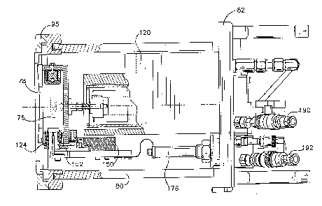
The ion generating source 12 (Figs. 2-5) embodying the present
invention includes a source block 120 supported by a rear wall 82 of the
source
housing 80. The source block in tum supports the plasma arc chamber 76 and
an electron emitting cathode 124 that in the preferred embodiment of the
present invention is supported by but electrically isolated from the arc
chamber
76.
A source magnet (Not Shown) encircles the plasma arc chamber 76
(Figures 14-18) to confine the plasma generating electrons to tightly
constrained
travel paths within the chamber 76. The source block 120 also defines cavities
that accommodate vaporizer ovens 122, 123 that can be filled with vaporizable
solids such as arsenic that are vaporized to a gas and then injected into the
plasma chamber 76 by means of delivery nozzles 126, 128. The plasma
arc chamber 76 is an elongated metal casting which defines an interior
ionization region R bounded by two elongated side walls 130a, 130b top and
bottom walls 130c, 130d and a front wall defining plate 132 that abuts the
ionization region R. Extending outwardly from its two side walls 130a, 130b
the
arc chamber includes a support flange 134 for mounting the arc chamber.
The plate 132 is aligned relative to the source housing 80.
As described in U.S. patent no. 5,420,415 to Trueira,
CA 02216818 2001-11-15
7
the plate 132 is attached to an aligning fixture 95 that~attaches to the
housing 80. Briefly, the alignment fixture 95 is inserted into the source
housing
such that the plane of the fixture is perpendicular to the ion beam axis. Once
in
position the ion source couples to the alignment fixture by being captured on
bullet head pins P (Figure 4) attached to the alignment fixture.
Four elongated bolts 136 threaded at their ends pass through four
openings 138 in the flange 134 and engage threaded openings 140 in the
source block 120. The bolts 136 pass through bushings 146 and springs 148
that bias the arc chamber 78 away from the source block 120 to facilitate
capture of the arc chamber by the alignment fixture 95.
Four pins 150 (only one of which is seen in Figure 8) extend through
openings 151 in the four corners of the arc chamber's flange 132. These pins
are spring biased away from the source block 120 by means of springs 152.
Slightly enlarged ends 150a of the pins fit within the plate 132 and keep the
plate and arc housing 76 connected together.
Vaporized material is injected into the interior of the plasma arc chamber
76 from the support block 120 by the delivery nozzles 126 , 128. On opposite
sides of the chamber 76 passageways 141 extend from a rear of the chamber
76 through a chamber body and open into the interior of the plasma arc
chamber 76. Additionally, gas can be directly routed into the~chamber 76 by
means of a port or opening 142 in a rear wall 130e of the chamber. A nozzle
144 abuts the opening 142 and injects gas directly into the arc chamber 76
from
a source or supply external to the ion source.
The wall 130d defines an opening 158 sized to allow the cathode
124 to extend into an interior of the plasma arc chamber 76 without touching
the chamber wall 130d that defines the opening 158. The cathode 124 is
supported by an insulating mounting block 150 that is attached the rear of the
arc chamber. A cathode body that fits into the opening 158 is mounted to a
metal mounting plate 152, supported by the insulating mounting block 150.
The cathode body is constructed from three metallic members 160, 162,
164. An outer tubular member 160 of the cathode 124 is made from a
molybdenum alloy material. A lower end 161 of the tubular member 160 that
CA 02216818 1997-10-16
g
abuts the mounting plate 152. An inner tubular member 162 is also made from
a molybdenum alloy material and has a threaded lower end portion 163. The
threaded end portion 163 of the inner tubular member 162 is threaded into a
threaded opening 167 in the mounting plate 152. The tubular members
160,162 are preferably cylindrical.
An end cap 164 (Figure 13) of the cathode 124 is conductive and is
made from a tungsten material. The cap 164 fits within a counterbore of an end
of the tubular members 162. The counterbore has an inwardly extending ridge
having an inner diameter slightly smaller than the diameter of the cap 164.
During assembly of the cathode 124 the cap is press fit into the tubular
member
162 and frictionally held in place during operation of the ion implanter 10.
The
length of the inner and outer tubular members 160, 162 is selected so that the
cap 164 extends upward into the arc chamber 76 beyond the end of the outer
tubular member 160.
Two conductive mounting arms 170, 171 support a filament 178 inside
the cathode 124. The arms 170, 171 are attached directly to the insulating
block 150 by connectors 172 that pass through the arms to engage threaded
openings in the block 150. Conductive energizing bands 173, 174 are coupled
to the filament and energized by signals routed through the flange 82 of the
housing 80 via power feedthroughs 175, 176.
Two clamps 177a, 177b fix a tungsten filament 178 within a cavity C
defined by the innermost tubular member 162 of the cathode. The filament 178
is made of a tungsten wire bent to form a helical loop (See Figure 5). Ends of
the filament 178 are supported by first and second tantalum legs 179a,179b
held in electrical contact with the two arms 170, 171 by the clamps 177a,
177b.
When the tungsten wire filament 178 is energized by application of a
potential difference across the power feedthroughs 175, 176 the filaments emit
electrons which accelerate toward and impact the cap 164 of the cathode 124.
When the cap 164 is sufficiently heated by electron bombardment, it in turn
emits electrons into the arc chamber 76 which strike gas molecules and create
ions within the chamber 76. An ion plasma is created and ions within this
plasma exit the opening 78 to form the ion beam. The cap 164 shields the
CA 02216818 2001-11-15
filament from contact with the ion plasma within the chamber and extends the
life of the filament. Additionally, the manner in which the filament is
supported
facilitates replacement of the filament.
Electrons generated by the cathode 124 that are emitted into the arc
chamber 76 but which do not engage a gas molecule within a gas ionization
zone move to the vicinity of a repeller 180. The repeller 180 includes a metal
member 181 located within the arc chamber 76 which deflects electrons back
into the gas ionization zone to contact a gas molecule. The metal member 181
is made of molybdenum. A ceramic insulator 182 insulates the repeller member
181 from the electrical potential of the lower wall 130c of the plasma arc
chamber 76. The cathode 124 and repeller 180 are therefore electrically and
thermally isolated from the arc chamber walls. Shorting of the repeller member
181 is impeded by a metal cup 184 that prevents ions from coating the
insulator
182.
The walls of the chamber 76 are held at a local ground or reference
electric potential. The cathode, including the cathode end cap 164 is held at
a
potential of between 50 - 150 volts below the local ground of the chamber
walls.
This electric potential is coupled to the plate 152 by a power feedthrough 186
for attaching an electrical conductor 187 to the plate 152 that supports the
cathode. The filament 178 is held at a voltage of between 200 and 600 volts
below that of the end cap 164. The large voltage difference between the
filament and the cathode imparts a high energy to the electrons leaving the
filament that is sufficient to heat the end cap 164 and thermionically emit
electrons into the chamber 76. The repeller member 181 is allowed to float at
the electrical potential of the gas plasma within the chamber 76.
The '006 patent to Sferlazzo et al depicts a schematic of a circuit that
controls arc current between the cathode and the anode (chamber walls of the
arc chamber). The operation of this circuit is described in the Sferlazzo et
al
patent. During generation of ions, the source heats up due to the injection
of ionizing energy into the arc chamber. Not all of this energy ionizes the
gas within the arc chamber and a certain amount of heat is generated.
The chamber includes water couplings 190, 192 that route
CA 02216818 1997-10-16
. ;: ~;
.~,~f~ii~~
cooling water into the source block and route heated water away from the
region of the arc chamber.
Insulating Block 150
In addition to insulating the cathode from the arc chamber the insulating
block 150 positions the filament 178 with respect to the cathode body and the
cathode body with respect to the arc chamber. Figures 9-12 depict the
insulating block 150 in greater detail.
The insulating block 150 is an elongated ceramic electrically insulating
block constructed from 99% pure alumina (A1203). The insulating block has a
first generally flat surface 200 that extends the length and width of the
insulating
block. This surface 200 engages a cathode mounting flange 202 (Figure 17)
that extends from the rear wall 130e of the gas confinement chamber 76. On a
side of the insulating block opposite the first surface 200, the insulating
block
150 defines a generally planar cathode support surface 210 for supporting the
cathode 124 and a second generally planar filament support surface 212 for
supporting the cathode filament 178 in spaced relation to the cathode. As seen
most clearly from the plan view of figure 9, the cathode support surface 210
has
two corner notches 220, 221 having openings 222, 223 that extend through a
reduced width of the insulating block defined by the notches.
Two connectors 224 having enlarged heads 225 extend through these
openings 222, 223 and attach the insulating block to the flange 202 on the arc
source chamber 76. The connectors 224 are threaded along their length.
These connectors engage threaded openings 204 in the flange 202. A backing
plate 206 (Figure 7) also includes threaded openings into which the connectors
extend to securely fasten the insulating block 150 to the arc chamber 78.
When the insulating block 150 is attached to the arc chamber the first
generally
flat surface 200 extends at a generally perpendicular angle to the back wall
130e of the arc chamber. Two locating pins 203 extend away from a surface
202a of the flange 202. These pins fit into corresponding openings 226 that
extend into the surface 200 of the insulator 150 to help align the insulating
block
150 during installation.
CA 02216818 1997-10-16
~~; ..r:;,
m . ; ~b~!,~~.
1, t. :t,uti~:
y
11
As seen in the Figures the metal plate 152 that supports the three piece
cathode body rests against the cathode support surface 210 of the block and
extends away from that surface to.bring the cathode body into alignment with
the opening 158. Threaded connectors 228 extend into a two recessed wells
230 in the surface 200 of the insulating block 150 and pass through openings
232 in the block to engage threaded openings 234 in the plate 152.
Two locating pins 236 are carried by the plate 152. As the plate is
attached to the insulating block 150 these pins extend into alignment holes
238
in the block 150. This helps align the block and plate and facilitates
connection
of the two during fabrication of the cathode as well as during maintenance of
the cathode after. use in the implanter 10.
Once the plate 152 is attached to the block 150 and the block attached
to the arc chamber the threaded opening 167 in the plate 152 that positions
the
three piece cathode body is aligned with respect to the opening 158 that
extends through the wall 130d in the arc chamber.
Planar surfaces 240 of the elongated legs 170, 171 engage and are
supported by the insulating block surface 212 that is spaced from the surface
200 by a maximum thickness of the insulating block 150. Threaded connectors
250 having enlarged heads extend through openings 252 in the legs 170, 171
and thread into threaded openings 254 in the filament support surface 212. As
seen most clearly in Figure 7, the relative spacing between the two planar
surfaces 210, 212 of the insulating block defines a gap G between the surface
240 of the legs 170, 171 and a surface 262 of the plate 152. This gap and the
fact that the ceramic is made of an electrically insulating material
electrically
isolates the two legs not only from each other but from the plate 152 that
supports the cathode body. The holes in the filament support legs 170, 171
align with the holes in the insulating body 150 and accurately position the
filament 178 within the inside of the cathode body.
As seen in Figures 9 - 12, the ceramic insulating body of the insulator
defines a number of elongated notches or channels N1 - N3. These notches
disrupt the generally planar surfaces of the insulating block 150. When
mounted near the arc chamber, the insulating block is coated with ions. The
CA 02216818 1997-10-16
;~ ;
12
insulators disclosed in U.S. patent no. 5,497,006 to Sferlazzo et al were
subject
to surface coating during operation of the source. This coating could lead to
premature arc-over or shorting and failure of the source. The channels N1-N5
in the single block insulator 150 make the block self-shadowing i.e. the ions
do
not coat a continuous surface across the insulating block and are therefore
less
prone to arc over.
Cathode Cap 164
The cathode cap 164 is a machined tungsten thermionic emitter that
provides arc current to the arc chamber. The simple disk shaped cap disclosed
in United States patent number 5,497,006 to Sferlazzo et al is replaced with a
cap 164 compatible with the cathode structure shown in the '006 patent.
The cap 164 has a reduced diameter emitting surface 165 and a wider
flange surface 166 that rests against an end of the inner tubular member 162.
The cap 164 significantly reduces thermal load of the support including
the insulating block 150. The cap also more efficiently utilizes filament
heating
power since less heating power is required to energize the filament 178 for a
given arc chamber current. The cap allows higher arc currents to be achieved
using the existing arc chamber controller electronics. Use of the cap has
resulted in increased production efficiency of all ion species, particularly
multiply
charged ions. For singly-charged ion, efficiency is increased by a
demonstrated
increase in dissociation of molecular ions( e.g., dissociation of BF3 and
BF2).
The combination of higher electron current density (due to the reduced
emission
area) and higher emitter temperatures (due to smaller thermal mass and
improved emitter thermal isolation) also results in higher fractions of
multiply-
charged ions.
From the above description of a preferred embodiment of the invention,
those skilled in the art will perceive improvements, changes and
modifications.
Such improvements, changes and modifications within the skill of the art are
intended to be covered by the appended claims.