Note: Descriptions are shown in the official language in which they were submitted.
CA 02216889 2002-12-17
A SOFT SWITCHED PWM AC TO DC CONVERTER WITH
GATE ARRAY LOGIC CONTROL
TECHNICAL FIELD
The present invention relates generally to power
supplies, and more particularly, to a high-efficiency pulse-
width-modulated AC to DC power converter for use in a DC
power supply system for telecommunications eqmipment.
BACKGROUND OF THE INVENTION
It is generally recognized that there are benefits
to be realized by operating pulse-width--modulated (PWM)
converters at high frequencies. High-frequency operation
permits lower cost and lighter weight converters to be
constructed. Soft switching permits even higher switching
frequencies. In order to successfully realize a PWM that
operates at high frequencies, however, it is necessary to
achieve very precise control of the PWM switches and to
precisely synchronize the different converters used in the
power supply. While many designs for such power supplies
- 1 -
CA 02216889 1997-09-26
have been invented, to date a design which enables PWM
control and converter synchronization precise enough fo-r an
efficient and robust power supply has not been developed.
SUMMARY OF THE INVENTION
It is an object of the invention to provide an AC
to DC power converter which uses a gate array logic
integrated circuit to time and condition PWM signals for
driving converters used in a power supply in order to
achieve soft switching which minimizes component stresses.
It is another object ofthe invention to provide
an AC to DC converter which uses a gate array logic for
providing converter synchronization signals reduce electron-
magnetic induction (EMI).
It is a further object of the invention to provide
an improved soft switched power supply -which uses power
boost and forward DC/DC converter topologies to provided
stable DC output even when the voltage of the ACinput
fluctuates.
These and other objects of the invention are
realized in a soft switched PWM AC to DC converter,
comprising:
a power factor corrector converter with a boost
topology that operates at a first fixed frequency;
- 2 -
CA 02216889 1997-09-26
a DC/DC converter with a forward topology that operates
at a second fixed frequency;
a clock that operates at a fixed frequency that is
greater than the first fixed frequency and the second fixed
frequency; and -
a gate array logic IC for timing and synchronizing PWM
signals for the power factor corrector converter and the
DC/DC converter using the clock signal, whereby the clock
signal is divided "n" times in the gate array logic IC using
a synchronous divider to provide digital timing signals for
use in converter synchronization and gate signal soft
switching.
The power supply in accordance with the invention
incorporates three converters. The converters include a
Power Factor Corrector (a boost topology) and a DC/DC
converter (a forward topology). A fly-back converter serves
as an auxiliary power supply for supplying operating current
to the power supply control components. In order to achieve
a high-quality stable DC- output substantially free from
noise and harmonics, it is necessary to-exercise precise
control over the PWM for switching those converters and to
synchronize the operation of each converter to reduce EMI
noise. To date, such control has not been realized because
the logic required-to exercise precise control is complex.
The present invention overcomes this problem by using a gate -
- 3 -
CA 02216889 1997-09-26
array logic IC, available from hattice Semiconductor Corp.,
Hillsboro, Oregon, U.S.A., and- a unique method for
controlling the PWM and synchronizing the converters.
In particular, a very high frequency clock signal
is input to the gate array logic IC asa data signalas well
as a clock signal. The data signal is divided using
synchronous division to achieve a digital timing signal that
may be described as a virtual monostable output which
provides an extremely precise timing signal- preferably
having a cycle of 1/64 of the total period resolution. The
digital timing signal permits very precise synchronization
of the three converters to minimize noise and harmonics. In
addition, the gate array logic IC is used to throttle the
DC/DC converter to a 50% duty cycle.- This eliminates the
requirement for a throttled PWM chip which permits the use
of a more robust chip that generates considerably less noise
and therefore ensures more precise PWM control.
The gate array logic IC is also used for analyzing
operating conditions in order to provide finer power supply
control. The gate array logic IC generates enabling signals
to enable and disable the PWM for the Power Factor Corrector
and the DC/DC converter based on outputs from a low-line
sensor, a high-line sensor, a low-bulk sensor, a high-bulk
sensor, a temporary release sensor and a high-voltage
shutdown sensor. The high-line and low-line sensors detect
- 4 -
CA 02216889 1997-09-26
input voltages which are outside the limits for which the
power supply was designed. The high-bulk and low-bulk
sensors indicate a problem at the Power Factor Corrector.
The high-voltage shutdown indicates a p-roblem at the load.
The invention therefore provides an efficient,
robust, light-weight controller which is particularly useful
for making -power supplies for telecommunications
applications.
BRIEF DESCRIPTION OF THE DRAWINGS
The invention will now be further explained by way
of example only and with reference to thefollowing drawings
wherein:
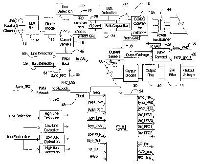
Fig. 1 is a schematic block diagram of a power
supply in accordance with the invention; and
Fig. 2 is a schematic block diagram of the gate
array logic IC and the principal inputs to and outputs from
the gate array logic IC.
DETAILED DESCRIPTION OF THE PREFERRED EMBODIMENT
Fig. 1 shows a schematic block diagram of a power
supply in accordance with the invention. A detailed
description of the components of the power supply are
provided in a related application ENTITLED CONTROLLER SYSTEM
FOR A DC POWER SUPPLY which is assigned to the applicant and
CA 02216889 2001-08-10
was filed on 25 September 1997.
The power supply in accordance with the invention
is generally indicated by the reference 10. An AC input 12
includes a line, neutral and chassis. The AC input passes
through an electromagnetic interference (EMI) filter 14 and
a rectifier (diode bridge) 16. A recitified input current
is sensed by a first current sensor 18 in order to shape it
and a voltage sensor to permit control of line bulk at the
same time, as will be explained below. A first called a
Power Factor Corrector (hereinafter PFC 22) with a boost
topology well known in the art is indicated by reference 22.
The PFC 22 is driven by conditioned drive signals output by
a gate array logic IC (hereinafter referred to as GAL 24) as
will be explained below in more detail. The output of the
PFC 22 is input to a second converter having a forward
topology, also well known in the art. The forward converter
includes the DC/DC converter switches 26, a power
transformer 34 and the output diodes 40. Positioned between
the PFC 22 and the DC/DC converter switches 26 is a third
converter, a fly-back converter 28 which is controlled by a
fly-back PWM as will also be explained below in more detail.
The fly-back converter 28 functions as an auxiliary power
supply. It uses energy stored in the bulk capacitors 30 to
- 6 -
CA 02216889 1997-09-26
output operating current to the control circuitry for the
powersupply 10. Located between the fly-back converter 28
and the DC/DC converter switches 26 is a bulk capacitor 30,
a bulk-detection circuit 32 and a ground 34, the function of
each of which is well understood in the art.
The DC/DC converter switches 26 are connected to a
power transformer 34 to isolate input line from output load
which is rectified by the output diodes 40 to give a desired
DC output voltage, typically -48 volts for use in
telecommunications applications. Connected to the line side
of the power transformer 34 through a current transformer 36
is a second current sensor 38 which outputs current to the
PWM chip for the DC/DC converter switches 26 as will
likewise be explained below in more detail. The output of
the forward converter passes through an output filter 42 and
an EMI filter 44, each of which is also well understood in
the art.
As explained above, the PFC 22, the DC/DC
converter switches 26 and the fly-back converter 28 are each
switched by a PWM signal generated by- a respective PWM IC
which outputs signals under the control of the GAL24. The
signals output by each PGVM IC for thePFC 22 and the DC/DC
converter switches 26 are conditioned by the GAL 24. The
operation of all three converters is synchronized by signals
also output by the GAL 24, as will be explained below in
CA 02216889 1997-09-26
more detail. The PFC 22 is switched by a PWM boost IC 46.
A gating signal is output by the PWM boost IC 46. The-
gating signal is stepped down by a voltage divider and wfed
into the GAL 24. The output from the PWM boost IC 46 is too
coarse to be used to drive the PFC 22 directly. It is
therefore conditioned by the GAL using frequencies derived
from a high-speed clock 48 which preferably operates at a
frequency of 6.4 MHz as -will be explained below with
reference to Fig. 2. The GAL 24 generates the necessary OFF
time for the PWM's output signal using synchronization
pulses generated from the clock frequency for the timing in
the period of the natural resonant oscillation of the line
current. The PFC 22 preferably operates at a fixed
frequency of 400 KHz. The output of the PWM boost_IC 46 is
controlled by a line detection input 50 for current shaping,
a bulk detection input 52 for bulk control, a synchronizing
signal Sync PFC 54for EMI reduction output by the GAL 24
and an enable signal PFC Ena 56 also put by GAL 24. The
shape of the input current should be the same as the line
voltage. The proper shape is a sine wave. The bulk
detection. input is to control the DC voltage across the bulk
capacitors 30. -
The DC/DC converter switches 2& are switched by a
PTr~M gate signal output by a PWM forward IC 48 which is
controlled by output voltage and the output current from the
_ g _
CA 02216889 1997-09-26
second current sensor 38 and by a synchronizing signal
Sync FWD 58 output by the GAL 24 and an enable signal
FWD Ena 60 also output by the GAL 24. The DC/DC converter
switches 26 operate at a fixed switching frequency of
200 -KHz. The PWM Forward IC 48 performs peak current mode
control using pulse-by-pulse current limiting to regulate
the peak output inductor current. The output current is
sensed by the second current sensor 38 and the output
voltage of the current sensor is added to a compensating
ramp to eliminate variation--in average output inductor
current due to changes in the duty cycle. The PMW Forward
IC 48 is disabled when the GAL 24 applies a high-level
signal to the FWA Ena 40.
The fly-back converter 28 is switched by a PWM
Fly-back IC 62 which outputs a PWM signal that is fed
directly to - the fly-back converter 28. The fly-back
converter 28- serves as an auxiliary power supply to provide
power to all the ICs and contro-1 and monitoring circuits.
The fly-back converter 28 uses energy from the bulk
2-0 capacitors 30 to supply three outputs, a +6.5V primary
output, a +12V primary output and a +12V secondary output.
Fig. 2 shows a block diagram of the GAL 24 and its
principal inputs and outputs. As explained above, the
clock 48 preferably operates at a frequency of 6.4 MHz. The _
clock output is used as a clock for the GAL 24 and is also
- g -
CA 02216889 1997-09-26
used as a data input to pin 31 of the GAL 24 where it is
passed through a series of synchronous dividers which_divide
the current frequency a desired number- oftimes to produce
an appropriate timing signal. Preferably, the 6.4 MHz clock
signal is synchronously divided five times to produce a
timing signal that is 1/64 of -the total period resolution.
The GAL 24 therefore is enabled to function as at least one
virtual monostable that generates digital timing signals
resulting from the synchronous division of the clock. By
using synchronous division of the 6.4 MHz clock signal, an
extremely accurate timing signal is produced which permits
precise control of the PWM timing forsoft switching 72 and
converter synchronization signals 68. While considerable
logic is required to realize the virtual monostables enabled
by the GAL 24, the GAL 24 has an adequate number of logic
gates to permit the synchronous division of the clock
inputs. This represents a significant- advance- in power
supply control. The synchronous division is accomplished
using frequency dividers 64. Output of the frequency
dividers is shaped by signal shaper 66 and output to a
converter synchronization signal circuit 68. To synchronize
the fly-back converter 28 (see Fig. 1), a 312.5 nanosecond
pulse is required. To synchronize the PFC 22 and the DC/DC
converter switches 26, a 78.125 nanosecond pulse is
required. The PFC 22 and the fly-back converter 28
_ 10 _
CA 02216889 1997-09-26
synchronization signals are timed so that the fly-back
converter 28 operates exactly at a frequency four times less
than the frequency of the PFC 22 to ensure that they do not
interfere with each other. The synchronization pulse for
the DC/DC converter switches 26 are -generated so that the
PFC 22 diodes conduct as much as possible while the DC/DC
converter switches 26 are ON to decrease the current in the
bulk capacitors 30 between the two converters. The
frequency of theDC/DC converter switches 26 is exactly one
half of the frequency of the PFC 22.
The operation of the PFC 22 requires extremely
accurate control of the transistors to ensure that soft
switching is attained. Only accurate control of the PWM and
synchronization of the three converters permit this topology
to operate efficiently and robustly. While such control and
synchronization requires complex circuitry, the GAL 24
provides an adequate number of logic gates to permit the
degree of control required. The output of the PWM ICs 46
and 48 (see Fig. 1) indicated by reference 70 is input to
the GAL 24 which uses frequencies generated by the frequency
dividers 64 to condition the PWM timing for soft switching.
The conditioned signals are output as gate signals 74 to the
PFC 22 and the DC/DC converter switches 26. The PWM Forward
IC 48 must operate at a maximum duty cycle of 50~ to control
that converter. If a throttled PWM IC is used, there is a
CA 02216889 1997-09-26
noise problem because commercially available throttled PWM
ICs incorporate a D flip flop which operates with the output
of !Q connected at the D input to change the output state at
each pulse of the clock. This type of throttling is called
asynchronous frequency division. It generates a noise at
the clock pin which can generate t~.ao inverter signals on any
given clock cycle. In order to overcome this problem, PWM
throttling is shifted to the GAL 24 and an unthrottled PWM
IC is used. This permits the use of a more robust PWM IC,
while ensuring substantially noise-free control of the PWM
duty cycle. Furthermore, commercially available PWM ICs
that are duty cycle throttled donot reach a 50% duty cycle
in operation. However, the GAL 24 permits a full 50o duty
cycle to be attained under any operating condition. This
means -that the primary side of the forward converter can be
optimized.
The other principal function of the GAL 24 is
operating condition analysis which is conducted by an
operating condition analysis routine 76 that receives line
and bulk detection inputs 78 from -the line detection
sensor 20 and the bulk detection sensor 32 (see Fig. 1).
Inputs are also received as a temporary release (TR)
signal 80 and a high-voltage shutdown ~HVSD) signal 82. The
operating condition analysis routine 76 analyzes these
inputs and outputs enabling signals PFC Ena 56 and
- 12 -
CA 02216889 1997-09-26
FWD Ena 60 (see Fig. 1) which are input to the PWM boost
IC 46 and the PWM Forward IC 48, respectively. When the PWM
Ics are reset they generate a soft start of the PFC 22 and
the forward converter. The GAL 24 also outputs an AC fail
alarm when the line detection sensor 20 senses that the AC
current on the input line 12 is interrupted.-
A reset routine 86 receives inputs from a start-up
circuit 88. The start-up circuit 88 initiates a reset of
all devices when the supply voltage reaches 4.5V. At that
point, the start-up circuit 88 sends a signal to the GAL 24
indicating that start-up has occurred. The PFC 22 and the
DC/DC converter switches 26 are disabled during the start-up
ofthe fly-back converter 26.
The PFC 22 and or the DC/DC converter switches 26
Z5 must be disabled when certain problems are detected on the
line, the load, the PFC 22, when a Temporary Release (TR) 80
is generated by the controller or a High Voltage Shutdown
(HVSD) condition occurs. Table I lists the potential
problems that may occur and the actions which are taken with
respect to each converter for each specific problem:
- 13 -
CA 02216889 1997-09-26
TABLE I
Power Factor Corrector DC/DC Converter
Low Line disable enable
High Line disable disable
Low Bulk enable disable
High Bulk disable disable
TR disable disable
HVSD enable disable
The high-line and low-line alarms respectively
detect when the input voltage is outside the limits for
which the power supply was designed. Those alarms generate
a -AC fail alarm to the controller and preferably turn on a
red LED to indicate a fail condition. The high-bulk and
low-bulk indicate a problem at the PFC 22. The HVSD
indicates a problem on the load.
The preferred embodiment of the controller as
described above is intended to be exemplary only. Changes
and modifications to the described embodiment may be
apparent to those skilled in the art. The scope of the
invention is therefore intended to be limited solely by the
scope of the appended claims.