Note: Descriptions are shown in the official language in which they were submitted.
CA 02217177 1997-10-O1
1
S P E C I F I C A T I O N
DRIVE METHOD AND DRIVE CIRCUIT OF DISPLAY DEVICE
TECHNICAL FIELD
This invention relates to a drive method and drive circuit
intended to compensate for degraded picture quality of moving
image in a display device so designed as to display multitonal
image signal making up one frame with plural subframes of
different relative ratios of brightness.
BACKGROUND TECHNOLOGY
The PDP (Plasma Display Panel) has recently attracted
public attention as a thin, light-weighted display device.
Completely different from the conventional CRT driving method,
the drive method of this PDP is a direct drive by digitalized
image input signal. The brightness and tone emitted from the
panel face depend therefore on the number of bits dealt with.
The PDP may be roughly divided into AC type and DC type
methods whose basic characteristics are different from each
other. As for the tonal display, however, 64-tone display was
the maximum reported from the trial manufacture level. The
Address/Display Separation type drive method (ADS subframe
method) has been proposed as an approach to solve this problem.
Figures 1(a) and 1(b) show the drive sequence and drive
waveform of the PDP used in this ADS subframe method.
In Figure 1(a), which gives an example of 256 tones, one
' CA 02217177 1997-10-O1
2
frame is composed of eight subframes whose relative ratios of
brightness are 1, 2, 4, 8, 16, 32, 64 and 128, respectively.
Combination of this brightness of eight screens enables a
display in 256 tones.
In Figure 2(b), the respective subframes SFl to SF8 are
composed of the address duration AD1, ... that write one screen
of refreshed data and the sustaining duration ST1, ... that
defines the brightness level of these subframes. In the
address duration, a wall charge is formed initially at each
pixel simultaneously over all the screens, and then the
sustaining pulses are given to all the screens for display.
The brightness of the subframes is proportional to the number
of sustaining pulses to be set to the predetermined brightness.
Two hundreds and fifty-six tones display is thus performed.
In such an AC drive method, the greater the number of
tones, the number of bits of the address duration as
preparation time for the panel to emit light and brightness
within one frame duration becomes. This relatively shortens
the sustaining duration as emission time, lowering thus the
maximal brightness.
Hence, the brightness and tone emitted from the panel face
depend on the number of bits to be dealt with With the
increased number of bits of the signal processed, the picture
quality improves, but the emission brightness reduces. If, on
the contrary, the number of bits of the signal processed is
diminished, the emission brightness augments, but the tonal
display reduces, deteriorating thus the picture quality.
CA 02217177 1997-10-O1
3
The error variance processing intended to minimize the
grayness error between input signal and emission brightness
reducing rather the bit number of output drive signal than that
of input signal is a processing to represent a pseudo
intermediate (half) tone, which is used when representing the
grayness with fewer tones.
In the conventional general error variance processing
circuit, the image signal of n-bit (n being 8 for instance)
original pixels Ai, j enters an image signal input terminal,
and passes through vertical adder and horizontal adders.
Further, in the bit conversion circuit, the image signal
reduces its bit number to m (4, for instance, and m < n).
After passing through the PDP drive circuit, it emits light
from the PDP.
The error variance signal from said horizontal adder is
compared with data stored beforehand by an error detect circuit,
and the difference between this signal and the data is weighted
by predetermined coefficient in an error load circuit. The
error detect output is added to said vertical adder through the
intermediary of the h line delay circuit that outputs the
reproduction error Ej-1 produced at the pixel going back by h
lines from the original pixel Aj, i, for example, by one line
in the past, and at the same time, added to said horizontal
adder through the intermediary of a d-dot delay circuit that
outputs the reproduction error Ei-1 produced at the pixel going
back by d lines from the original pixel Ai, j, for example, by
one dot in the past. In general, the coefficients at said
CA 02217177 1997-10-O1
4
error load circuit are to be set so that their total sum may be
i (one) .
As a result, a stepwise emission brightness level
represented by 4 bits is output momentarily at the output
terminal of the bit conversion circuit. Nevertheless, the
emission brightness levels above and below the step-like level
are actually output alternately in predetermined proportion,
which will be recognized as an averaged state. This allows for
a correction brightness line with approximate y=x.
However, the subframe lighting method was problematical in
that the picture quality- worsens in a part of screen when the
input level of original signal somewhat changes.
In a case where 4-bit image signal scanning from SF4 to
SF1 in the sequential order of brightness as shown in Figure 2
(a), the level 7 is quantized by 0111 and 8 is quantized by
1000 when 'the input of the first and second frames of the
original signal change at levels 7 and 8, respectively. At the
point of change from 7 to 8, therefore, the level becomes
01111000 as shown in Figure 2(b) with indiscriminate emission
at the levels 7 and 8. The brightness at that time reaching
about 2 times the level 7 or level 8, it looks like a white
1 i ne.
Conversely at the point of change from 8 to 7, the level
becoming 10000111, the non-emission duration looks like a
continuous black line.
The sampling signal a before conversion as shown in Figure
3(c) and the signal b converted into the waveform of ADS
CA 02217177 2001-07-31
subfield method as shown in Figure 3(d) were filtered by the
LPF (Low Pass Filter) with the half of frame frequency as the
cutoff frequency and comp ared. The comparison of these signals
revealed a large difference between the point of change of the
5 image signal level from 7 to 8 and the point of change from 8
to 7 as shown in Figure 3 (e), where A represents the LPF output
wavef orm of a, and B, that of b:
In such a display and reproduction system where the image
signal is time-shared into plural subframes, there exists at a
point of level change a level that does not always coincide
with the change of original signal when a moving image charging
in the time axial direction is displayed_ This was
problematical since it degrades the picture quality.
It was problematical particularly because pseudo-half tone,
for example, by an error variance in one tone level was
accompanied by flickering in the time axial direction.
The first purpose of this invention is to provide a method
to compensate for the degradation of picture quality of a
moving image arising from the half-tone display of the subframe
method.
D I SCLOSURE OF TT~E I NVEIv'T I ON
The drive method of a display device by this invention
consists in that in a display unit so designed as to display a
mufti-tone image signal composing one frame from plural
subframes of different relative ratios of brightness, two
subframes or minimal brightness are arranged adjacently to each
CA 02217177 2001-07-31
6
other so that the subframe selection and lighting may be
possible in response to the change of image brightness in the
time axial direction.
When, for example, the level of original signal changes
from 7 to 8 or from 8 to 7, the brightness of 5-bit 5-screens
is used, SF3, SF2, SF1 and SF1 of 4, 2, 1, and 1 are selected
as the subframes for level 8, and SF3, SF2 and SF1 of 4, 2 and
1 are selected as subframes for level 7.
More materially, when one frame changes from level 7 to 8,
or from 8 to 7, the level 7 is quantized at [01110] by SF3, SF2
and SF1 out of SF4, SF3, SF2, SF1 and SF1, whi 1 a the 1 eve 1 8 i s
quantized at [01111] by SF3, SF2, SF1 and SF1 out of SF4, SF3,
SF2, SF1 and SFl. At the point of change from level 7 to 8.
the 1 eve 1 becomes [0l 110] [O 1 11 1] , and the lighting effect is
discontinuous at the levels 7 and 8. At the point of change
from 8 to 7, the level becomes [01111] [01110] and the non-
lighting effect is discontinuous. The brightness at these points does
not therefore change greatly, which prevents the picture
quality from being deteriorated.
The drive method for display device by this invention is
characterized in that a correction circuit which corrects the
original image signal is provided to annihilate the difference
between the original image signal and emission brightness
before processing the signal by the subfield drive method. The
correction circuit has an M frame delay circuit which delays by
M frame or frames (M beir_g any positive integer, M=1 for
example) and outputs an original image signal, a correction
CA 02217177 1997-10-O1
7
constant set circuit that sets, for each pixel, a correction
data intended to eliminate the difference between the original
image signal and emission brightness arising from the subfield
drive method, based on the original image signal and M frame
delay circuit, and an adder that adds the original image signal
to the correction data output by the correction constant set
circuit into the image signal forming the subject of the
processing by the subfield drive method.
The memory (ROM for instance) in the correction constant
set circuit stores beforehand the correction data intended to
measure the feature representing the relationship between the
original image signal and emission brightness for the display
panel on which the image is displayed by the subfield drive
method and to annihilate the difference between the original
image signal and emission brightness as obtained for each pixel
of the display panel based on the measured data. For example,
data "1" with image signals "7" and "8" as addresses is stored
as correction data when the level of the image signal changes
from "7" to "8", wherein "7" is the image signal (image data)
going back by M frame (if M=1) or frames and "$" is the image
signal of current frame.
Based on the image signal going back by M frame or frames
that M frame delay circuit outputs (for instance, the signal of
level °7" going back by one frame) and the image signal of
current frame (for instance, signal of level "8"), the
correction constant set circuit reads out (with the signals of
level "7" and level "8" as addresses} and outputs correction
~ CA 02217177 1997-10-O1
8
data ("1" for example) from the incorporated memory (ROM, for
examp 1 e) . The adde r adds the image s i gnal ( "8" f or examp 1 e)
of current frame to the correction data output from the
correction constant set circuit ("1" for example) and adopts
the added value ("9" in this example) as the input image signal
to the display device. We may thus eliminate the difference
between the original image signal and emission brightness
arising from the subfield drive method.
BRIEF EXPLANATION OF THE DRAWINGS
In Figure 1, (a) represents a drive sequence of 8-bit 256
tones according to the ADS subfield method, and (b) illustrates
a drive waveform in Figure 1(a).
In Figure 2, (a) depicts a conventional 4-bit 16 tone
drive sequence by ADS subfield method, and (b) the drive
waveform at the point of change from 7 to 8, or 8 to 7 by the
drive sequence in Figure 2(a).
Figure 3 illustrates a distortion by the display device,
where (a) represents the level of original image signal (4-bit),
(b) sampling points, (c) sampling signal a before change, and
(d) signal b as converted from signal a by the ADS subfield
method, and (e) LPF output waveform A and B of signals a and b.
In Figure 4, (a) shows a 5-bit drive sequence in the first
embodiment of the drive method by this invention, while (b)
exhibits the drive waveform at the point of change from level 7
to 8, or 8 to 7 by the driving sequence in Figure 4(a).
In Figure 5, (a) schematically shows a 6-bit drive
CA 02217177 1997-10-O1
9
sequence in the second embodiment of the drive method by this
invention, while (b) diagrammatically shows up a drive sequence
at the point of change from level 15 to 16, or from 16 to 15 by
the drive sequence in Figure 5(a).
Figure 6 illustrates the distortion by the display device
by this invention, where (a) shows the of original 4-bit image
signal, (b) sampling points, (c) sampling signal a before
change, (d) the signal c as converted by the ADS subfield
method after the correction of signal a by the correction
circuit, and (e) represents the LPF output waveforms of signals
a and c.
Figure 7 is a block diagram that shows up an embodiment of
the drive circuit for display unit according to this invention.
BEST EMBODIMENT TO CARRY OUT T~ INVENTION
The objects of the invention will be seen by reference to
the description of the first embodiment of the driving method
for display device according to the invention, taken in
connect i on wi th F i gures 4 (a) and 4 (b) .
When 1 frame consists of four subframes as in Figure 4(a),
conventionally these subframes were SF4, SF3, SF2 and SFl whose
relative ratios of brightness were 8, 4, 2 and 1 respectively.
In this invention, one frame includes four subframes SF4, SF3,
SF2, SF1 and additionally another SF1, and their relative
ratios of brightness being 8, 4, 2, 1 and 1, respectively. The
two SF1 with the least brightness ratio are arranged adjacently
to each other.
CA 02217177 2001-07-31
1 0
When the level of original signal is changed from 7 to 8,
or from 8 to 7 (when the variation is minimal), the brightness
of 5-bit 5-screens is used.
In an embodiment wherein 16 tones are displayed using the
combination of brightness of 5-bit 5-screen as shown in Figure
4 (b) when the level of original signal is changed from 7 to 8
or from 8 to 7, the level of the first frame at the original
signal being 7, the succeeding SF3, SF2 and SF1 are selected
out of 5 subframes SF4, SF3, SF2, SF1 and SF1 whose relative
rat ios of br i ghtness are 8, 4, 2, 1 and l, respect ive ly and the
level 7 is quantized by [01110].
When the level of next frame is changed to 8, the
succeeding SF3, SF2, SF1, and SF1 are selected out of 5
subframes SF4, SF3, SF2, SF1 and SFl whose relative ratios of
I5 brightness are 8, 4, 2, 1 and 1, respectively and the level 8
is quantized by [01111]. In consequence, the level becomes
[01110] [01111] as in Figure 4 (b) at the point of change from
level 7 to 8, the lighting at the levels 7 and 8 being thus
discontinuous.
Similarly, at the point of change from level 7 to 8, the "lighting effect", or
the
light emitting duration decreases due to discontinuity, or [0l 110] [01111 ]
as shown in
Figure 4b, thus reducing luminescence compared to the example of Figure 2(b).
As the
point of change from level 8 to 7 the "non-lighting effect", or the light
emitting duration
increases due to discontinuity or [0l 111 ] [01110], thus increasing
luminescence
compared to the example of Figure 2(b).
CA 02217177 2001-07-31
1 OA
The picture quality thus does not degrade because there is no great change in
brightness at these points of change.
Referring now to Figures 5 (a) and 5 (b), we are going to explain the second
embodiment.
In the Fieure 5 lal by the inventiennne frame inrlnc~Pc
CA 02217177 2001-07-31
1 1
six subframes SFS, SF4, SF3, SF1 and additionallyanother
SF2,
SF1,and their relative ratios brightness are 16, 4, 2,
of 8, 1
and 1, respectively. The last subframes SFl and having
two SF1
the least brightness ratio 1 arranged adjacently to each
are
other.
At a point where the level of original signal changes from
15 to 16, the 1 eve 1 becoming [011110] [011111] as shown in
Fi gure 5 (b) , the 1 i ght i ng effect at the levels 15 and 16 i s
discontinuous.
Similarly at a point where the level of original signal
changes from 16 to 15, the level becoming [011111] [011110] as
shown in Fi gur a 5 (b) , the non-1 i ght i ng effect at the levels 16 and 15
is discontinuous.
Since the lighting from 16 to 15 and non-lighting from 16
to 15 are both discontinuous, the brightness at these points is
not subject to any great change, preventing thus the picture
quality from being degraded.
In general, the foregoing embodiment may be expressed as
f o 1 1 ows.
One frame consists of n bits. The frame comprises
therefore n subframes whose relative ratios of brightness are
2°-', 2'-z, . ~ , 2°-~ c-°' . 2° of the suhframe
pith tha loa~r
relative brightness ratio 1 is added adjacently to the 2° of
the last subframe with least brightness ratio 1 above. Thus 2°
tones will be displayed making use of the combination of the
brightness of (n'-1) 'bits (n+1) screens.
Wrie:: the level of origir_al signal is charged from [~°-'_1,,
' CA 02217177 1997-10-O1
1 2
to [2°-1] or from [2°-1] to [2°-I-1] (when the variation
is the
least), the brightness of the (n+1) bits (n+1) screens is used,
and SF[2°-2], SF[2°-s], ~~~, SF[2°-"c=°'] are
selected as the
subframes for level [2°-1], while SF[2°-2], SF[2°-3],
~~~, SF
[2°-° c=~> ] are selected as the subframes for level [2"-I-1].
As has thus far been described, this invention does not
allow the picture quality to degrade despite certain change of
input level of the original signal because, in a display unit
so designed as to display multitonal image signal by
constructing one frame from plural subframes of different
relative ratios of brightness, two subframes of minimal
brightness are arranged adjacently to each other, and the
subframes are selected and lighted up in response to the change
on image brightness in the time axial direction.
We now explain an embodiment of the drive circuit for
display unit by this invention.
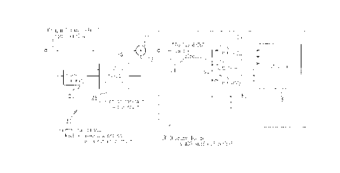
Referring now to Figure 7, the numeral 10 represents an
example of display device by known ADS subfield (an example of
subfield driving method), which has a display drive control
circuit 14 coupled with an image signal input terminal 12, and
PDP18 coupled with the output side of this display drive
control circuit 14 through the intermediary of drive elements
161, 162, 163, ~ ~
The numeral 20 symbolizes a correction circuit peculiar to
this invention (a circuit intended to remove the distortion of
a moving image) that has the frame memory 24 as an example of M
frame delay circuit (case of M--1) coupled with the original
' CA 02217177 1997-10-O1
1 3
image signal input terminal 22, a correction constant set
circuit 26 connected to the output side of said memory 24 and
to said original image signal input terminal 22, and an adder
28 connected to the output side of said correction constant set
circuit 26 and to said original image signal input terminal 22.
The correction constant set circuit 26 is provided with
ROM30 as a memory, which stores beforehand correction data
intended to annihilate the difference- between the original
image signal and emission brightness due, for every pixel, to
the ADS subfield method in PDP18 whose image is displayed by
the ADS subfield method. Measured are the characteristics
representing the relationship between the original image signal
and emission brightness for the PDP18 whose image is displayed
by the ADS subfield method. Said correction data can be
obtained from this measured data.
When the level of image signal is changed from "7" to "8°
for example,wherein "7" is the level of the image signal
(image data)going back M frame (M=1 for instance) and
by "8" is
the level the image current frame, the correction
of of data
can be obtained from the characteristic data as measured. The
correction data ("1" for instance) thus obtained has been
stored beforehand in ROM30 with the image signal "7" and "8" as
addresses. Similarly, the correction data ("-1" for instance)
when the 1 eve 1 of image s i gnal changes f rom "8" to "7" i s
stored bef orehand in ROM30 wi th the image s i gnal s "8" and "7"
as addresses.
The foregoing correction constant set circuit 26 has been
CA 02217177 2001-07-31
1 4
so designed as to read out and output as set value the
correction data for each pixel of PDP18 from said ROM30 (data,
for example, of level "1") based on the original image signal
(signal of level "8" for instance) input into said original
image signal input terminal 22 and on the output signal (signal,
for example, of level "7") from said memory 24. The adder 28
has been so configured that it adds the original image signal
to the correction data that is output by the correction
constant set circuit 26, and outputs this added value to the
lfl image signal input terminal 12 of said display unit 10.
Concomitantly referring to Figure 6, we will now explain
the action of the foregoing embodiment. Our description will
be based on a suggestion that the correction data stored in
ROM30 is "0" (that is, no correction required) respectively
15 when the level of the original image signal as sampled for
corresponding pixel and for each frame is .. "("
'> >
"7" "8" . . , "g" "7" , "6" . . . , pr when th i s 1 eve 1 changes
from "6" to "7" and from "7" to "6" , ~d ~e correction data
as stored in ROM30 is "1" when the level changed from "7" to "8"
2~ and ~~_l~~ when the level changed from "8" to "7".
(a) When the level of the image signal as input into the
input terminal 22 one frame before is "7" and that of the
current frame is "8" the correction. constant set circuit 26
reads out the correction data "1" from the ROM30 with the
25 signals of levels "7" and "8" as addresses, and outputs this
data as set value to the adder 28.
' CA 02217177 1997-10-O1
1 5
(b) The adder 28 adds the correction data "1" as output
from the correction constant set circuit 26 to image signal
(level "8") of current frame as input into the input terminal
22, and outputs thi s data to the input terminal 12 of di spl ay
unit 10 as a corrected image signal (level "9").
(c) When the level of the image signal as input into the
input terminal 22 one frame before is "8" and that of current
frame is "7" the correction constant set circuit 26 reads out
correction data "-1" from ROM30 with the signals of levels "8°
and "7" as addresses and outputs this data as set value to the
adder 28.
(d) The adder 28 adds to the image signal (level "7") of
current frame input into the input terminal 22 the correction
data "-1" to be output from the correction constant set circuit
26, and outputs this data as corrected image signal (level "6")
to the input terminal 12 of display unit 10.
When consequently the original image signal whose level
changes as . . "6" "7" "8° ~ ~ "8" "7" "6" . . . for
~. . . . ~. . > >
each frame and for corresponding pixel is input into the input
terminal 22, corrected will be the difference between the
emission brightness and original image signal of PDP18 arising
from the ADS subfield method when the level changes from "7" to
"8" and from "8" to "7" From the correction circuit 20,
therefore, corrected image signal whose level changes as ~~~,
2 5 "6" "7" , "8" , ~ ~ ~ , "8" , "7" , "6" , ~ ~ ~ f o r a ach f r ame an d f
o r
corresponding pixel is input into the input terminal 12 of the
display unit 10.
CA 02217177 2001-07-31
16
As was the case with conventional embodiments, the display
unit 10 lights up and displays the PDP 18 with the signal
processing (signal conversion) by the ADS subfield method
through the drive control of drive elements 161, 162, 163,
by the display drive control circuit 14, when the difference
between the original image signal and emission brightness due
to the ADS subfield method is corrected by the correction
circuit 20, and this correction signal is input as image signal
into the input terminal 12. Hence a moving image can be
lfl displayed on the PDP18 without any distortion (pseudo contour).
We studied the image signal wherein the difference between
the original image signal and emission brightness due to the
ADS subfield method is corrected as above in a similar fashion
as in Figure 5. We passed the original image signal (sampling
signal) a before its being converted into the waveform of ADS
subfield method and the signal c which is the signal a as
corrected by the correction circuit 20 according to this
invention, then converted into the waveform by the ADS subfield
method, into the LPF (Low Pass Filter) with the half of the
frame frequency as the cutoff frequency to compare these two
signals. As shown in Figure 3(e), we could by far decrease the
distortion in the time axial direction at the change point of
image signal level from "7" to "8" and that from "8" to "7"
than the conventional one as shown in Figure 3;e).
In the foregoing embodiment, an explanation was made on
the case where this the M frame delay circuit is composed of a
frame memory that delays the circuit by one frame, but this
' CA 02217177 1997-10-O1
1 7
invention is not limited to this type of embodiment. Any M
frame delay circuit (M being a positive integer) will do if it
delays the original image signal by M frame or frames to output
the delayed signal.
In the foregoing embodiment, a correction data was set by
correction constant set circuit to annihilate the difference
between the original image signal and emission brightness of
display panel resulting from the ADS subfield method, and the
adder added original image signal to the correction data as
output by the correction constant set circuit for the display
unit to have the corrected image signal, but the invention is
not limited to this type of embodiment. The corrected image
signal to the display unit may be had by a correction constant
set circuit (correction image signal output circuit) provided
with the adding ability.
That is, a correction data may be set to eliminate the
difference between the original image signal and emission
brightness due to the ADS subfield method for every pixel,
based on the original image signal for each pixel of display
panel and on the output signal from the M frame delay circuit,
and the corrected image signal to the display unit may be had
providing a certain image signal output circuit that adds said
set correction data to the original image signal and then
outputs this data.
In the foregoing embodiment, an explanation was given
about the use of this invention on a display device by means of
the ADS subfield method, but the invention is not limited to
CA 02217177 1997-10-O1
1 8
this type of embodiment. The present invention may be used for
a display wherein one screen display duration of display panel
may be time-shared into the display duration of bit number N (N
being an integer not less than 2) corresponding to the
displayed tone, and the number of sustaining pulses for each
divided display duration may form the subject of a weighting
corresponding to each bit to display multitonal image (that is,
a display device by subfield drive method).
In the foregoing embodiment, an explanation has been given
on a case where the display panel o,f the display device is a
PDP, but this invention is not limited to this type of
embodiment. The invention may be used also for such a display
unit where the display panel is LCDP.
As has thus far been described, this invention gives a
correction circuit provided with a M frame delay circuit, a
correction constant set circuit and adder in order to correct
the original image signal before the signal processing by the
subfield drive method in a display unit so designed as to
display the multitonal image by the subfield drive method.
Further, the memory (ROM for instance0 in this correction
constant set circuit stores beforehand a correction data
intended to eliminate the difference between the original image
signal and emission brightness. This correction data intended
to cancel out the difference between the original image signal
and emission brightness may be obtained from the measured
values of original image signal and emission brightness on the
display panel whose image is displayed by, for example, the
' CA 02217177 1997-10-O1
1 9
subfield drive method. For instance, the correction data has
been stored as "1" when the image signal level changes from "7"
to "8" in such a fashion that the image signal level going back
by M frame or frames is "7" and the image signal level of
current frame is "8".
The correction constant set circuit reads out and outputs
correction data ("1" for instance) from the memory (ROM for
instance), based on the image signal going back by M frame or
frames that M frame delay circuit outputs (signal of level "7"
going back by one frame) and the image signal of current frame
(signal of level "8" for instance). The adder outputs, as
correction image data, to the display unit this correction data
plus the image signal of current frame ("9" for example). This
allows us to annihilate the difference between the original
image signal and emission brightness resulting from the
subfield drive method and remove the distortion of moving image
(pseudo contour).
INDUSTRIAL AVAILABILITY
This invention is effective particularly for the display
units that perform a pseudo-half tone display between one-tone
levels by error variance. w