Language selection

Search

Patent 2217324 Summary

Third-party information liability

Some of the information on this Web page has been provided by external sources. The Government of Canada is not responsible for the accuracy, reliability or currency of the information supplied by external sources. Users wishing to rely upon this information should consult directly with the source of the information. Content provided by external sources is not subject to official languages, privacy and accessibility requirements.

Claims and Abstract availability

Any discrepancies in the text and image of the Claims and Abstract are due to differing posting times. Text of the Claims and Abstract are posted:

  • At the time the application is open to public inspection;
  • At the time of issue of the patent (grant).
(12) Patent Application: (11) CA 2217324
(54) English Title: CONNECTION DEVICE FOR SWITCHING ELECTRICAL SIGNALS
(54) French Title: DISPOSITIF DE CONNEXION POUR COMMUTATION DE SIGNAUX ELECTRIQUES
Status: Deemed Abandoned and Beyond the Period of Reinstatement - Pending Response to Notice of Disregarded Communication
Bibliographic Data
(51) International Patent Classification (IPC):
  • H01R 29/00 (2006.01)
(72) Inventors :
  • BORSETTO, GIANCARLO (Switzerland)
  • POLETTI, BRUNO (Switzerland)
(73) Owners :
  • GIANCARLO BORSETTO
  • BRUNO POLETTI
(71) Applicants :
  • GIANCARLO BORSETTO (Switzerland)
  • BRUNO POLETTI (Switzerland)
(74) Agent: ROBIC AGENCE PI S.E.C./ROBIC IP AGENCY LP
(74) Associate agent:
(45) Issued:
(86) PCT Filing Date: 1996-04-25
(87) Open to Public Inspection: 1996-10-31
Availability of licence: N/A
Dedicated to the Public: N/A
(25) Language of filing: English

Patent Cooperation Treaty (PCT): Yes
(86) PCT Filing Number: PCT/IB1996/000378
(87) International Publication Number: IB1996000378
(85) National Entry: 1997-10-22

(30) Application Priority Data:
Application No. Country/Territory Date
1221/95-8 (Switzerland) 1995-04-28

Abstracts

English Abstract


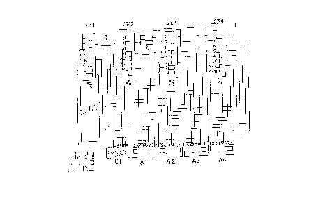
A connection device (1) for switching electrical signals, comprising: (a)
primary offtakes (A1, A2, A3, A4) with multiple contacts, with at least one
pair of conductors carrying an incoming signal leading to each of these; (b) a
multiple incoming plug or point (C1) fitted with an equivalent number of
contact terminals to the aforesaid conductors carrying a signal, which are
connected to the said terminals; (c) a multiple outgoing plug or point (C12)
connected to the incoming multiple plug or point (C1); (d) the same number of
outgoing conductors as there are contact terminals on the said outgoing plug
or point (C12) forming pairs each carrying an outgoing signal; (e) secondary
offtakes with multiple contacts (A12, A22, A32, A42), with at least one pair
of outgoing conductors carrying an outgoing signal leading to each of these,
also comprising a means (SW1, SW2, SW3, SW4, SW12, SW22, SW32, SW42, Ti, Qi)
of selective, reversible connection of pairs of terminals on the incoming plug
or point (C1) to pairs of contacts on the primary offtakes (A1, A2, A3, A4)
and pairs of terminals on the outgoing plug or point (C12) with pairs of
contacts on the secondary offtakes (A12, A22, A32, A42).


French Abstract

Un dispositif de connexion (1) conçu pour la commutation de signaux électriques comprend: (a) des sorties primaires (A1, A2, A3, A4) à plusieurs contacts, pourvues d'au moins une paire de conducteurs acheminant un signal entrant jusqu'à chacune de celles-ci; (b) une prise ou point d'arrivée multiple (C1) doté d'un nombre équivalent de bornes de contact sur les conducteurs acheminant un signal, ces conducteurs étant connectés aux bornes; (c) une prise ou point de sortie multiple (C12) connecté à la prise ou point d'arrivée multiple (C1); (d) le même nombre de conducteurs de sortie qu'il y a de bornes de contact sur la prise ou point de sortie (C12) formant des paires, chacune acheminant un signal sortant; (e) des sorties secondaires à plusieurs contacts (A12, A22, A32, A42), dotées d'au moins une paire de conducteurs de sortie acheminant un signal sortant jusqu'à celles-ci. Ce dispositif comprend également un organe (SW1, SW2, SW3, SW4, SW12, SW22, SW32, SW42, Ti, Qi) de connexion réversible, sélective de paires de bornes sur la prise ou point d'arrivée (C1) connectant des paires de contacts sur les sorties primaires (A1, A2, A3, A4), ainsi que des paires de bornes sur la prise ou point de sortie (C12) pourvu de paires de contacts sur les sorties secondaires (A12, A22, A32, A42).

Claims

Note: Claims are shown in the official language in which they were submitted.


CLAIMS
1. Connection device (1) for switching and receiving low
voltage electrical signals, comprising:
(a) a set of primary offtakes (A1, A2, A3, A4) with multiple
contacts, with at least one pair of conductors carrying an
incoming signal leading to each of these;
(b) a multiple incoming plug or point (C1) fitted with
contact terminals equivalent in number to the said conductors
carrying the incoming signals, which are connected to the
said terminals;
(c) a multiple outgoing plug or point (C12) designed to be
connected to the said incoming multiple plug or point (C1)
respectively and with an equivalent number of contact
terminals;
(d) the same number of outgoing conductors as there are
contact terminals on the said outgoing plug or point (C12)
forming pairs each carrying an outgoing signal, each
conductor being connected to one of these terminals;
(e) a series of secondary offtakes with multiple contacts
(A12, A22, A32, A42) for utilisation of the signals, with at
least one of the said pairs of outgoing conductors carrying
an outgoing signal leading to each of these;
characterized by the fact that it also includes a means (SW1,
SW2, SW3, SW4, Ti) of selective, reversible connection of
pairs of contact terminals on the said plug or multiple
incoming offtake (C1) respectively with the same number of
pairs of terminals as the said primary offtakes (A1, A2, A3,
A4) to which the said pairs of conductors carrying incoming

signals lead, and a means (SW12, SW22, SW32, SW42, Qi) of
selective, reversible connection of pairs of contact
terminals on the said of offtake or multiple outgoing plug (C12)
respectively, to which the said outgoing conductors lead and
the same number of pairs of contacts as the said secondary
multiple-contact offtakes (A12, A22, A32, A42) for
utilisation of the signal.
2. A device according to Claim 1 in which all the pairs of
conductors carrying an incoming signal are joined together in
a single cable, termed the incoming cable.
3. A device according to one of Claims 1 or 2, in which all
the pairs of conductors carrying an outgoing signal are
joined together in one cable, termed the outgoing cable.
4. A device according to one of Claims 1 to 3 in which the
said means of selective, reversible connection of pairs of
contact terminals consists of sets of switches (SW1, SW2,
SW3, SW4 and SW12, SW22, SW32, SW42) with multi-function
contacts and/or diverters and sections of electrical circuit
(Ti, Qi) which connect these electrically to the various
contact terminals of the component parts of the device
itself.

Description

Note: Descriptions are shown in the official language in which they were submitted.


CA 02217324 1997-10-22
W O 96/34432 PCT~B96/00378
Connection Device for Switching Electrical Siqnals
Thi~ invention concerns the field of electrotechniCal
applications, with particular regard to the reception and
switching o~ electrical signals (nor~lly low voltage) used
for the trAn~ission of data, pictures, ~ound, etc.
These ~ignal~ are currently sent to ~everal primary offtake~
with multiple contacts: although the-ce o~ft~kec each have at
lea6t four pairs o~ co~tact6, usually only one of these pair~
is used, and from these there is only one outgoing pair
(known popularly as cdoublets~) of conductor wires car~ying a
gi~en input signal. The pairs of wire~ which lead, a~
stated, to the primary offta~e~ are then connected to a
multiple t~rm;n~l connection element (plug or point).
In current practice, four of these prima~y o~ftake~ are used,
with a total of eight conductor wires leading, as me~tioned,
to a connection p~ug or point with eight te ~i n~ls.
The latter i8 then connected to a further offtake or plug,
respectively, with an equi~alent number of ter~in~l6, from
which a further eight cable~ lead, forming four doublets each
of which i5 then connected to a ~ingle offtake, which can be
termed the secondary offta~e to ~i6tinguish it from the
a~orementioned primar~ offtakes, and this acts a~ an outgoing
offtake to utlli~e the signals which reach it.
From the description given thufi far, it can be seen that tv
switch ~ust four ilLC~ ing ~ignals, a total of eight offtakes
w~th eight terminals has to be u~ed ~four for incoming
signal~ and ~our for outgoing ~ignals3 connected by means of
connection companent~ with eight poles.
t In addition, once one of the ~econdary of~take~ for the

CA 02217324 1997-10-22
W 096/34432 PCTnB96/00378
outgoing signals is connected ~uch that it c~n receive a
gi~en ~Lgnal recelved a~ an incom~ ng ~gna~ by on~ of the
said primary offtakes, thi~ ~ituation remain~ locked
virtually p~ -nontly under the ef~ect~ of time ~on~traintC.
Finally, in order to reduce the disadvantages of this signal
switohi~g and receiviny system, modi_ications are made to the
connecting offtake~plug pairs, ~etting pair~ of t- in~ls in
electrical ~ontact which lead to different <do~blet~ in a
predetermin~ mode, different from those in the origin~l
arrangement, by means of el~ctric~l cbridgos~ or ~imilar
devices.
In addition, both the aforementioned pr~mary and second~ry
offtake~ are under-used, with many of the contact terminAls
not connected to any signal.
To eliminate the dLsad~antages de~cribed above, the in~entor
of this in~ention has devised a connection deYic~ for the
reception or switchi n~ 0~ electrical signals which, as well
a~ comprising the co~ponen~ part~ descrlbed pre~iou81y and
corresponding to the state of the art, i5 characterised by
the fact that it also includes a means of selective,
reversible connection of pair~ o~ contact term~nAl~ on the
multiple o~tgoin~ offtake, o~ plug respectively, with the
same number of pairs of terminals a~ the ~aid primary
offta~es to which the ~aid pairs of conductors carrying
incoming ~ignals lea~, and a means o~ selecti~e, re~ersi~le
connection of pairs of contact t~rminAls on the ~aid outgoing
multiple offtake or plug, respecti~ely, to which the outgoing
conductor~ lead and the ~ame n~l~ho~ of pairs of contacts on
the saLd secondary multLple contact of~ta~es for utilisation
of the signals.
A description is now giYen of a pref~rred example of

CA 02217324 1997-10-22
W O 96/34432 PCTAB96/00378
con~truction of the device as per the invention, in which
reference is al~o made to the attached drawings which ~how:
Figure 1, the wiring diagram of the part of the device
comprising four prLmary offtakes and an incoming connecting
plug or point with set~ of switches;
~igure 2, the wiring diagram of the part of the device
comprising four xecondary offtakes and an outgoing connect~ng
plug or point that can be connected to the s2id incoming
connecting plug or point, and a further net of switches;
F~ 7U_~ ~, th~ _.~m.a~ d~ag~m ~o.m~.priaing th~ t~ ~ ri ~,~
layout~ in Figure~ 1 and 2 connected to each other by means
of ~ connector element.
Looking at Figure 1, there are four primary offtakes A1, A2,
A3 and A4, with eight conductors le~ g to each of th~se
(designed to form four doublet~ carrying an e~ui~alent number
of electrical signal~ ) which can be connected selectively and
re~ersibly to a c~nn~ctor element (plug or point) Cl by mean~
o~ four sets of multiple ~wLtches S~1, SW2, SW3, SW4 with
multi-function contactY, ie arranged, ~or example, in such a
way as to con~ect dif ~erent conductor wires depending on
whether these are actuated (~On> position~ or not (<Off>
position).
Other type~ of co~~onent, such as switche~ and/or diverters
w~th sliding contacts or similar can he used for this
purpo~e.
In the al~ov.~ ?~tLoned FLgure 1, for example, the contact
terminal 1 of the incoming plug C1 can be connected
selecti~ely and rever~i~ly to contact 1 o~ th~ primary
offtake Al, or contact 4 of the prLmary offtake A2, or to

CA 02217324 1997-10-22
W 096/34432 PCT~B96/00378
contact 3 of the latter. Thi~ i~ achieved by actuating in
c~iff~rent way~; the variou~; ~witche~i ~ 8 in the figure),
forming part of the switch ~et SW1.
A s~mi~ar operation can likewise be carried ou~ for all the
~inin~ contacts of the primary offta~e8, connecting them
in a predet~m~1n~d mAnn~ to the t~-n~l~ on plug Cl by
means of the other swltch ~ets SWZ, SW3 and SW4.
In Pigure 2 again, the 6a~e operation can be applied,
connecting the contact terminals of ths plug C12 in a
predete- in~ seguence and mode, to the various contact~ on
the ~econdary outgoing o~ftakes Al2s A22. A32 ! A42 bY
~elective actuation of the switches forming th~ switch sQts
- SW12, SW22, SW32 and SW42.
For example, by connecting, a~ ~hown in the Figures, t~rmin~l
l of the multiple plug C12 with contact 4 of the secondary
offtake A22 (connecting ~witch 2 of ~et SW12 and
disconnect~ng switches l and 3), this co~n~ts contact 4, by
means of the mul~iple plug C1, with contact 1 of the prlmary
offtake Al, or with one of the contact~ 3 or 4 of the primary
offtake A2, depending on how the conncction was configured in
line with the preceding part of the explanation.
Thi~ provid~s a connection device for ~witching and receiving
signals that is flexible in zpplication, economic in co~t and
swi~t and ea~y to actuate, thu~ achie~ing the ~tated purpose
of the invention.
The termin~ls of all the pr~mary and secondary of~t~ke~ can
al~o thu~ be ~ully ~tillsed.
A~ already stated, the switches described thus far can be
~ubstituted with other types, for example with ~liding

CA 02217324 1997-10-22
W 096/34432 PCT~B96/00378
cont~ct~, or with diverters or change-over switches more
~uited to the dif~erent de~ign ~equirement~.
Figure 3 ~hows a complete wiring diagram of the device
described, consisting of two part~ as shown in Figures 1 and
2, interconnected by means of the plug Cl~offtake C12 pair.
Any con~truction that differs from the examples de~;cribed so
far, which aro not limitative or bin~ing, but ~ attributable
to t~e concept~ expressed in t~e sttached claims, shall
nonethele~s ~e deemed to ~e covered by the protection granted
by this applicAtion for patent.
The different conductors connecting the primary or secondary
o~ta~es to the re~pectiYe plugs and points can of course be
~oined to form sections of connecting and linking ca~le, or
assembled in other ways.

Representative Drawing
A single figure which represents the drawing illustrating the invention.
Administrative Status

2024-08-01:As part of the Next Generation Patents (NGP) transition, the Canadian Patents Database (CPD) now contains a more detailed Event History, which replicates the Event Log of our new back-office solution.

Please note that "Inactive:" events refers to events no longer in use in our new back-office solution.

For a clearer understanding of the status of the application/patent presented on this page, the site Disclaimer , as well as the definitions for Patent , Event History , Maintenance Fee  and Payment History  should be consulted.

Event History

Description Date
Time Limit for Reversal Expired 2002-04-25
Application Not Reinstated by Deadline 2002-04-25
Deemed Abandoned - Failure to Respond to Maintenance Fee Notice 2001-04-25
Letter Sent 2000-05-04
Reinstatement Requirements Deemed Compliant for All Abandonment Reasons 2000-04-20
Deemed Abandoned - Failure to Respond to Maintenance Fee Notice 1999-04-26
Classification Modified 1997-12-24
Inactive: IPC assigned 1997-12-24
Inactive: First IPC assigned 1997-12-24
Inactive: Notice - National entry - No RFE 1997-12-11
Inactive: Applicant deleted 1997-12-11
Inactive: Inventor deleted 1997-12-11
Application Received - PCT 1997-12-09
Application Published (Open to Public Inspection) 1996-10-31

Abandonment History

Abandonment Date Reason Reinstatement Date
2001-04-25
1999-04-26

Maintenance Fee

The last payment was received on 2000-04-20

Note : If the full payment has not been received on or before the date indicated, a further fee may be required which may be one of the following

  • the reinstatement fee;
  • the late payment fee; or
  • additional fee to reverse deemed expiry.

Patent fees are adjusted on the 1st of January every year. The amounts above are the current amounts if received by December 31 of the current year.
Please refer to the CIPO Patent Fees web page to see all current fee amounts.

Fee History

Fee Type Anniversary Year Due Date Paid Date
Basic national fee - small 1997-10-22
MF (application, 2nd anniv.) - small 02 1998-04-27 1998-04-24
MF (application, 4th anniv.) - small 04 2000-04-25 2000-04-20
Reinstatement 2000-04-20
MF (application, 3rd anniv.) - small 03 1999-04-26 2000-04-20
Owners on Record

Note: Records showing the ownership history in alphabetical order.

Current Owners on Record
GIANCARLO BORSETTO
BRUNO POLETTI
Past Owners on Record
None
Past Owners that do not appear in the "Owners on Record" listing will appear in other documentation within the application.
Documents

To view selected files, please enter reCAPTCHA code :


To view images, click a link in the Document Description column (Temporarily unavailable). To download the documents, select one or more checkboxes in the first column and then click the "Download Selected in PDF format (Zip Archive)" or the "Download Selected as Single PDF" button.

List of published and non-published patent-specific documents on the CPD .

If you have any difficulty accessing content, you can call the Client Service Centre at 1-866-997-1936 or send them an e-mail at CIPO Client Service Centre.

({010=All Documents, 020=As Filed, 030=As Open to Public Inspection, 040=At Issuance, 050=Examination, 060=Incoming Correspondence, 070=Miscellaneous, 080=Outgoing Correspondence, 090=Payment})


Document
Description 
Date
(yyyy-mm-dd) 
Number of pages   Size of Image (KB) 
Abstract 1997-10-21 1 72
Description 1997-10-21 5 183
Drawings 1997-10-21 3 112
Claims 1997-10-21 2 65
Representative drawing 1998-01-04 1 15
Reminder of maintenance fee due 1997-12-29 1 111
Notice of National Entry 1997-12-10 1 193
Courtesy - Abandonment Letter (Maintenance Fee) 1999-05-24 1 186
Notice of Reinstatement 2000-05-03 1 171
Courtesy - Abandonment Letter (Maintenance Fee) 2001-05-22 1 182
PCT 1997-10-21 10 291
Fees 2000-04-19 1 30
Fees 2000-04-19 1 34
Fees 1998-04-23 1 30