Note: Descriptions are shown in the official language in which they were submitted.
CA 02217375 2000-04-20
FIELD OF THE INVENTION
This invention relates to synchronous dynamic
random access integrated circuit memories (SDRAMs) and
in particular to a method and apparatus for operating
data paths in SDRAMs.
BACKGROUND TO THE INVENTION
Asynchronous DRAMs are externally controlled by
a processor using standard RAS (row address sample), CAS
(column address sample), WE (write enable) and OE
(output enable) signals. Operational speed of such
asynchronous DRAMS is determined by the speed internal
circuits require to perform operations specified by the
control signals. The processor, however, must wait for
the asynchronous DRAM to complete the required
operation, since changing the control signals of the
memory address during operation of the DRAM would
interrupt its operation. As a result, the processor
must waste valuable time which it could otherwise use to
perform other tasks in the system, by being tied up
waiting for the memory. The discrepancy in operating
frequencies between that of the microprocessor (which
presently can be specified to operate at up to e.g. 500
MHz), and the typically maximum operating frequency of
asynchronous DRAMs .(,approximately 60 to 80 MHz) creates
a mismatch which is becoming increasingly intolerable
for many current applications.
In an attempt to increase the speed of the
system, a synchronous interface can be provided to
control the DRAM, the interface and DRAM together
forming a synchronous DRAM (SDRAM), which is well known
in the art. The use of latches for input and output
data as well as address and control signals, frees the
microprocessor from its waiting state, and allows it to
perform other functions while the SDRAM performs its
required operation under control of the system clock.
1
CA 02217375 2000-04-20
In the case of a read operation, for example, after a
predetermined number of clock cycles, the microprocessor
can access resulting data from the output latches of the
SDRAM.
Designers of data path architectures for both
DRAMS and SDRAMs have tended to favor use of a bi-
directional global data path, using a single global data
bus per bit for both read and write operations. The bi-
directional global data path has been favored in order
to minimize the amount of memory chip area used for
conductive data paths.
However, the read and write operations may have
different speeds and different requirements on the
global data bus. For example, the bus turn-around time
between a read operation and a write operation may be
too large for the SDRAM cycle time to accommodate. The
read operation may be faster than the write operation,
or vice versa. In either case, these requirements can
be resolved by physically separating the global data bus
into distinct read and write global data buses. This
resolves bus contention problems, since the two buses
operate independently and mutually exclusive of one
other. However, this architecture incurs a substantial
chip area penalty, due to the requirement to provide a
second global data bus structure for the entire die.
The penalty becomes increasingly severe for buses which
carry wide data word widths.
SUMMARY OF THE INVENTION
The present invention returns to the
architecture of a single global data bus which carries
both read and write data. However, it receives or
provides data to output circuitry which can interface an
external processor, at a uniform read or write
frequency.
In an embodiment of the invention, a double
local data bus structure is used, interfacing the global
data bus, which allows a column address to change on
2
CA 02217375 2000-04-20
every system clock cycle. The double local data bus
structure has two parallel local data paths which are
activated on alternate clock cycles, and therefore
operate at half the nominal operating frequency. For a
S read operation, the global data bus receive~~ the read
data from the local data bus, and carries the data
differentially at the system operating frequency. For a
write operation, the global data bus operates at half
the nominal operating frequency, with each global data
bus line of the data bus pair carrying alternate words
to be written in a single ended rather than differential
mode, and being dedicated to either one or the other
local data paths for every other clock cycle.
The processor will therefore see a uniform read
or write operating frequency, thereby simplifying its
interface with the SDRAM. Yet the amount of chip area
needed for the global data bus is minimized, since only
a single bi-directional global databus is required. The
global data bus is used in a manner toggling between
single ended databus lines at half the system frequency
for a write operation, and in a differential manner at
the system frequency for a read operation.
In accordance with an embodiment of the
invention, a method of operating data paths in a data
processing system having a global data path and a local
data path is comprised of (a) receiving input data at an
input node at a system clock frequency; (b) coupling
data received from the data input node in alternating
sequence to each of a global data bus and a complement
global data bus at a fraction of the system clock
frequency; (c) converting single-ended data on the
global data bus and its complement to differential data;
(d) alternately driving the differential data onto a
local differential data bus pair of a plurality of local
data bus pairs at one-half of the system clock
frequency; and (e) writing the data from the local data
bus pair into selected memory cells.
3
CA 02217375 2000-04-20
In accordance with another embodiment, a data
interface system for writing data to a memory via a
global data path and a local data path is comprised
of(a) a data input node for receiving single-ended data;
(b) a global data bus write driver for driving the
single-ended input data within the memory; (c) a
complementary global data bus pair for carrying, in an
alternating sequence, the driven single-ended input data
on each of the global data buses of the global data bus
pair; (d) a local data bus write driver for receiving
the driven single-ended input data from the each of the
global data buses of the global data bus pair and for
converting the single-ended input data into differential
local input data and for driving the differential local
input data onto differential local data buses.
BRIEF DESCRIPTION OF THE DRAWINGS
A better understanding of the invention will be
obtained by a consideration of the detailed description
below, in conjunction with the following drawings, in
which:
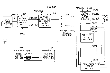
Figure 1 is a block diagram of parts of an SDRAM
which includes an embodiment of the invention,
Figure 2 is a schematic diagram of a global
write data bus select circuit,
Figure 3 is a schematic diagram of a glcbal data
bus write driver,
Figure 4 is a schematic diagram of a local data
bus write driver,
Figure 5 is a schematic diagram of a column
access and sense amplifier used for both read and write
operations, which is a circuit used in the prior art,
Figure 6 is a schematic diagram of a read sense
amplifier,
Figure 7 is a schematic diagram of a global data
bus sense amplifier used for read operations,
Figure 8 is a data path timing diagram for the
write operation, and
4
CA 02217375 2000-04-20
Figure 9 is a data path timing diagram for the
read operation.
DETAILED DESCRIPTION OF EMBODIMENTS OF THE INVENTION
Turning first to Figures 1 and 8, and
considering the single bit case, in a write operation,
data to be written is received from off-chip via an
input buffer and is latched to produce a single ended
mode input line DINCL-, and is applied to a global write
data bus select circuit 100. A clock signal BUSD is
also applied to select circuit 100 which operates at
one-half of the system clock frequency. The select
circuit 100 applies each alternate word to respective
single ended write lines WDB BO- and WDB B1-. A
schematic diagram of an embodiment of select circuit 100
is illustrated in Figure 2, and will be described in
more detail later.
The data signals carried on lines WDB BO- and
WDB B1- are applied to a global data bus tri-state write
drivers circuit 102, which is enabled by global data bus
write driver enable signals WEN~GDB and global data bus
precharge signals GDB PRE. Drivers circuit 102 drive
the global data bus pair comprised of lines GDB and
GDB-. A schematic diagram of an embodiment of global
data bus write driver circuit 102 is illustrated in
Figure 3, and will be described i~ more detail later.
It should be noted that a bit of each alternate
input data word is thus separately carried by alternate
global data lines GD:B or GDB- at one-half of the system
frequency. The global data lines are separately driven
as single ended lines carrying two streams of data, as
distinguished from mutually differential lines carrying
a single stream of data in complementary form.
The write data carried by each of the global
data bus lines GDB and GDB- is applied to different
local data bus write drivers 104A and 104B. The drivers
104A and 104B are enabled by block select signal BSEL
and by respective driver enable signals WDE BO and
S
CA 02217375 2000-09-29
WDE_B1. The local write drivers convert the single
ended data carried by the global data bus lines GDB and
GDB- to differential signals, which are applied to
respective local data bus pairs DB B0, DB BO-, and
DB_B1, DB_B1-.
A schematic diagram of an embodiment of driver
circuits 104A and 1048 is illustrated in Figure 4, and
will be described in more detail later.
The respective two local data bus pairs DB B0,
DB_BO- and DB_B1, DB_B1- are accessed in turn by a local
column (or bit line) select signal Y BO or Y B1 for
writing the data carried by the local data bus pairs
into a memory cell selected by a wordline (not shown). A
schematic diagram of an embodiment of sense amplifier
106 is illustrated in Figure 5, and will be described in
more detail later. Sense amplifier 106 is described in
U.S. patent 5,416,743 to Allan et al.
Thus in operation, successive data words carried
per bit by the DINCL- single ended input line are
coupled in an alternating manner to single ended write
data lines WDB BO- and WDB B1-, at a frequency specified
by the BUSD signal, preferably one half of the system
clock frequency. The write data lines are then applied
to global data bus tri-state write drivers at the same
rate, when enabled by signals WEN GDB and GDB PRE, to
drive global data bus lines GDB and GDB- in a single
ended manner with the signals carried by WDB BO- and
WDB_B1-.
After passing down the global data bus, the
signals are received by local data bus write drivers
104A and 1048, where the single ended signals are
converted to differential signals and are applied to
respective local data buses DB B0, DB BO- and DB B1 and
DB B1-. These signals are then written to the SDRAM
storage cells:
6
CA 02217375 2000-04-20
In a read operation, a data bit stored in a
selected storage cell of the SDRAM is sensed by the
sense amplifier 106, and is differentially applied to
either of the local data bus pairs DB B0, DB BO- or
DB B1, DB B1-, alternating on every clock cycle. The
signals thus carried by the local data buses are then
received by corresponding local data bus sense
amplifiers 108A and 108B at one-half of the system
frequency, and are applied in alternation, at the system
frequency, to global data bus lines GDB, GDB-, in
differential form.
After being carried by the global data bus, the
differential data is received by global data bus sense
amplifier 110, which further amplifies the differential
data and latches it, producing the output signals RDBL,
RDBL- and RDBP, RDBP-, for application to a data output
buffer 112 which will typically couple these signals to
an output pin of the SDRAM chip.
Thus it may be seen that the global bus lines
GDB and GDB- are used to carry in single ended form in
one direction, successive words of write data at one
half of the system frequency, and are used to carry in
differential form in the other direction, successive
words of read data at the system frequency. The write
data is input to the memory at the system frequency and
the read data is output from the memory at the system
frequency. Thus while only a single bi-directional
global data bus per bit is used , the chip can interface
a processor at the system frequency.
In order to ensure that the read and write data
do not interfere, a WRITE CL BK- (write block) signal is
applied to the local data bus sense amplifiers 108A and
1088 to inhibit application of data to the global bus
during a write operation, and similarly the global data
bus tri-state write drivers are disabled by WEN GDB
falling prior to a read operation.
7
CA 02217375 2000-04-20
Turning now to the detailed schematic diagrams,
Figure 2 illustrates the global write data bus select
circuit 100. The input data line DINCL- splits into two
lines, the data carried thereby passing through
respective inverters 200 and 202 into flip-flops 204 and
206 and 205 and 207 connected in master/slave
configuration, then passing through inverters 208 and
210 to respective single ended write data lines WDB BO-
and WDB B1-.
Each of the flip-flops is comprised of a pair of
cross-coupled inverters 214 and 216 in flip-flop 204,
and 218 and 220 in flip-flop 206. The input of inverter
214 is coupled to the output of inverter 200 via a full
CMOS transfer gate comprising of NMOS FET 213A and PMOS
FET 2138 having their sources and drains coupled
together in parallel in a well known manner. The input
of inverter 218 is similarly coupled to the output of
inverter 202 via another CMOS transfer gate consisting
of NMOS FET 215A and PMOS FET 215B having their sources
and drains coupled together in parallel.
The second stage flip-flops 205, 207 are
similarly cross coupled as are 204 and 206. They
receive inputs via two CMOS transfer gates 217A, 2178
for 205 and 219A, 2198 for 207. The two flip-flop
stages and their corresponding transfer gates act in a
master/slave configuration, effectively providing a two-
stage pipeline for each single ended write data line
WDB BO- and WDB B1-.
A clock signal BUSD is applied via inverter 212
to the gate of NMOS FETs 213A, 219A and to the gate of
PMOS FETs 2178, 2158 and from the output of inverter 212
and via inverter 211 to the gates of PMOS FETs 2138,
219B and the gates of NMOS FETs 215A, 217A. The clock
signal BUSD oscillates at half the system frequency.
Thus every successive half cycle of the BUSD clock
signal will alternately be logic high followed by logic
low, causing the transfer gates to be alternately
8
CA 02217375 2000-04-20
conductive. For example, when BUSD is high, 217B, 217A
and 215A, 215B are conductive, whereas when BUSD is low,
213A, 213B and 219A, 219B are conductive. The circuit
thus operates as a master/slave selection switch, with
the clock BUSD selecting which branch of the circuit
should carry the alternate data bit. As a result, data
appearing on line DINCL- at the full system frequency is
driven alternately onto WDB BO- or WDB B1- at half the
system frequency.
In summary, the input data to be written is
carried on single ended line DINCL- and is split into
two branches WDB BO- and WDB B1-. Each branch is
comprised of two series connected flip-flops, clocked by
the BUSD clock signal. This clock signal oscillates at
half the system frequency. As input data appears at the
full system frequency, the BUSD signal clocks this data
into each branch at half the system frequency. The BUSD
signal thus acts as a switch selection signal,
alternately switching the path of the input data onto
one or the other of the two branches. As a result, data
is alternately driven on to either of the WDB BO- or
WDB B1- lines at half the system frequency.
The WDB BO- and WDB B1- lines are input lines to
the global data bus tri-state write drivers, as shown in
Figure 3. The input. lines are respectively coupled
through inverters 300 and 302 to first inputs of NAND
gates 304 and 306. A g~.obal data bus precharge enable
signal GDB PRE is applied via inverter 308 to second
inputs of NAND gates 304 and 306. The output signals of
NAND gates 304 and 306 are respectively coupled to
inputs of NAND gates 310 and 312 as well as to inputs of
NOR gates 314 and 316.
The output of NAND gate 310 is coupled to the
gate of a PMOS FET 318, and the output of NOR gate 314
is coupled to the gate of NMOS FET 320. The source-
drain circuits of FETs 318 and 320 are connected in
series between a voltage supply Vcc and ground. A
9
CA 02217375 2000-04-20
global data bus line GDB is connected to the junction of
FETs 318 and 320.
The output of NAND gate 312 is coupled to the
gate of a PMOS FET 322, and the output of NOR gate 316
S is coupled to the gate of NMOS FET 324. The source-
drain circuits of FETs 322 and 324 are connected in
series between the voltage supply vcc and ground. A
global data bus line GDB- is connected to the junction
of FETs 322 and 324.
IO A write enable control signal WEN GDB is applied
to the inputs of inverters 326 and 328 via inverter 327,
the outputs of which are respectively coupled to another
input of NAND gate 310 and NAND gate 312. The output of
inverter 326 is coupled via inverter 330 to another
15 input of NOR gate 314, and the output of inverter 328 is
coupled via inverter 332 to another input of NOR gate
316.
In operation, the signals to be written appear
alternately on the lines WDB BO- and WDB B1-. With the
20 GDB PRE control signal at low logic level and WEN GDB at
high logic level, the WDB BO- and WDB B1- signals pass
alternately through NAND gates 304 and 306 to NAND gates
310, 312 as well as NOR gates 314 and 316, to drive the
gates of NMOS FETs 320 and 324 and PMOS FETs 318 and
25 322. The bus lines GDB and GDB- are thus alternately
driven between the logic states of the data signals and
ground, i.e. a single ended mode of operation, each at
one-half of the system frequency.
More specifically, and with reference to Figure
30 8, both the WDB BO- and WDB B1- signals start out
precharged high. As the first bit of data appears on
the input buffer, bit 0 on a first system clock cycle
rising edge, after a short delay, the bit 0 is latched
and appears on the DINCL- line. The BUSD clock signal,
35 oscillating at one-half of the system clock frequency,
rises causing the WDB BO- signal to become logic low.
This logic low is inverted by inverter 300 to provide
CA 02217375 2000-04-20
two high inputs to NAND gate 304, thereby causing a low
output, which in turn is fed as an input to NAND gate
310 and to NOR gate 314. Since WEN GDB is high, one of
the inputs to NOR gate 314 is set logic low. The output
of NAND gate 304 thus provides a second low input to NOR
gate 314, thereby causing it to provide a high output.
This high output causes NMOS pull down FET 320 to
conduct, thereby pulling the GDB line low. In the
meantime, the PMOS pull up FET 318 is non-conductive due
to its high input.
Similarly, the WDB Bl- branch will pass on data
to the GDB- line on the following transition of the BUSD
signal. As a second system clock inputs and latches the
second bit of incoming data, bitl, the BUSD signal
changes from high to low, thus causing the WDB B1 branch
to function similarly to the WDB BO- branch as described
above. In this alternating manner, on every clock cycle
the BUSD signal changes logic state and switches the
path of the incoming data from WDB BO- to GDB and
WDB B1- to GDB- respectively.
At the end of the write operation the PMOS pull-
up FETs 318 and 322 are briefly enabled by the GDB PRE
control signal passing through NAND gates 304 and 310,
and 306 and 312 and being coupled to their gates, to
cause the GDB and GDB- bus lines to receive the nominal
voltage Vcc, and thus become precharged.
After the GDB and GDB- bus lines have been
precharged, the signal WEN GDB should fall, ensuring
that the write drivers are tri-stated after the write
operation, thus allowing the global data buses to be
used to carry read data without interference.
The global data buses GDB and GDB- are used to
carry data significant distances along the memory chip,
for storage in the memory cells of the SDRAM. The
signals carried by single ended bus lines GDB and GDB-
are driven onto separate differentially operated local
data buses DB B0, DB BO- and DB B1, DB B1-. This local
11
CA 02217375 2000-04-20
driving function is carried out by local data bus write
drivers 104A and 104B. There are two local write
drivers per bit for each BO and B1 local data paths. A
circuit of a write driver is shown in Figure 4, of which
all are similar.
Data from the GDB line for the BO path or GDB-
line for the B1 path is applied via inverter 400 to the
sources of CMOS FET transfer gate transistor pair 402
which have their sources and drains connected in
parallel. The drains of FET pair 402 are coupled to a
latch comprised of a pair of inverters 404 connected in
back to back configuration. The output of the latch is
coupled to an input of a NOR gate 406 the output of
which is connected to the gate of a an NMOS FET 408 of
an NMOS pair having their source-drain circuits
connected in series between a voltage source Vdd and
ground. The other NMOS FET 410, has its source
connected to ground. The junction of the FETs 408 and
410 provides the local data bus output DB BO
corresponding to the GDB input and DB B1 corresponding
to the GDB- input. The drains of FET pair 402 is also
connected to an input of a NOR gate 407.
A write driver enable signal WDE BO for the GDB
input or WDE B1 for the GDB- input is applied to the
sources of another CMOS FET pair, which also have their
drains connected together. The drains are also coupled
through inverter 414 to another input of NOR gate 407 as
well as to another input of NoR gate 406.
The output of NOR gate 407 is coupled to the
gate of an NMOS FET 416 which has its source-drain
circuit connected in series with the source-drain
circuit of another NMOS FET 418, between a voltage
source Vdd and ground. The output of NOR gate 407 is
also connected to the gate of FET 410, and the output of
NOR gate 406 is also connected to the gate of FET 418.
The complementary local data bus line DB BO
corresponding to the GDB input or DB B1 corresponding to
12
CA 02217375 2000-04-20
the GDB- input is connected to the junction of FETs 416
and 418.
A block selection signal BSEL is coupled to the
gate of the NMOS FET of the pair 412, to an input of a
NAND gate 420, and via an inverter 422 to the gate of
the PMOS FET of the pair 412 as well as the gate of an
NMOS FET 424. The source of FET 424 is connected to
ground, and the drain of FET 424 is connected to the
drains of the FET pair 412.
The output of NAND gate 420 is coupled to the
gate of the PMOS FET of the pair 402, and through an
inverter 426 to the gate of the NMOS FET of the pair
402. The output of inverter 414 is coupled to the other
input of NAND gate 420.
In operation, prior to a write operation, the
block selection signal BSEL is low, as well as the write
driver enable signals WDE BO and WDE Bl. Upon the BSEL
signal going high, the gates of the FETs 402 cause those
FETs to conduct, allowing incoming data from the GDB or
GDB- global data bus to pass through and become latched
by the latch comprised of inverters 404. The latching
is necessary to allow the GDB/GDB- lines to be
precharged as soon as possible if a read is requested
following a write operation. After a predetermined
delay, the WDE BO or WDE B1 signal rises, which causes
the FETs 402 to become non-conductive, isolating the
input from the latch. The signal rising also passes
through FETs 412 to NOR gates 406 and 407, allowing the
data latch 404 in the latch to pass to the gates of FETs
408 and 416. The gates of FETs 410 and 418 are driven
with the logic level to be applied to the respective
opposite line, causing them to be oppositely conductive
to FETs 408 and 416. Thus lines DB BO or DB B1 and
DB BO- or DB B1- are driven differentially to nominally
Vdd or ground due to conduction of FETs 408 and 416, or
410 and 418. This occurs at half the system frequency.
13
CA 02217375 2000-04-20
Thus the single ended data carried separately on
each line of the global data bus is transferred to a
pair of differential local data buses DB B0, DB BO- and
DB_B1, DB_B1- each one of which carries data at half the
system frequency. The data carried by the local data
buses are applied to a selected memory cell location as
described in the aforenoted U.S. patent. A schematic
diagram of the preferred sense amplifier and columns
access circuitry is shown in Figure 5.
The pairs of local data buses are coupled to bit
lines (or columns) BL and BL- via the source-drain
circuits of FETs 500, 502 for data bus pair DB B0,
DB BO-, and via the source drain circuits of FETs 504,
506 for data bus pair DB B1, DB B1-. FETs 500 and 502
are enabled by their gates being coupled to enable line
Y B0, and FETs 504 and 506 are enabled by their gates
being coupled to enable line Y B1. Thus a control
signal applied to the Y BO line causes FETs 500 and 502
to conduct, transferring data carried by local data bus
pair DB B0, DB BO- to the bit line pair BL and BL-.
From here the data is written to a selected bit storage
cell (not shown).
Similarly, a control signal applied to the Y B1
line causes FETs 504 and 506 to conduct, transferring
data carried by local data bus pair DB Bl, DB B1- to the
bit line pair BL and BL-. From here the data is written
to a selected bit storage cell (not shown).
The control signals on the Y BO and Y B1 lines
are driven every alternate cycle, causing the sense
amplifier to write data alternately from each of the
local data buses once each system clock cycle.
This completes the write cycle.
Data is read by the local sense amplifier being
controlled to read data stored in a selected local bit
storage cell in a well known manner, at the system clock
rate. With reference to Figure 1 again, on a per bit
basis, the read data is applied alternately to each of
14
CA 02217375 2000-04-20
the local data buses DB B0, DB BO- and DB B1, DB B1- in
a manner reciprocal to the write operation, i.e. control
signals are applied to the lines Y BO and Y B1
alternately every second system clock cycle. The read
data is thus transferred to and is carried by the local
data bus lines in differential form. Local data bus
sense amplifiers 108A and 108B, each coupled to a
respective local data bus, sense the read data and apply
it differentially and alternately to global data bus
lines GDB and GDB- in single ended form, at one-half of
the system clock frequency.
Figure 6 illustrates a schematic diagram of a
local data bus sense amplifier 108A, 108B, and Figure 9
illustrates a signal timing diagram for the read
operation. Data from the local data bus lines DB B0,
DB BO- and DB B1, DB B1- are applied to inputs of
differential sense amplifier 600. The outputs of sense
amplifier 600 are coupled via inverters 602 and 604 to
the gates of respective NMOS FETs 606 and 608. The
source-drain circuits of FETs 606 and 608 are connected
in series with the source-drain circuits of FETs 610 and
612 respectively, the series circuits being connected
respectively between the bi-directional global data bus
lines GDB, GDB- and ground. This illustrates the
transition between the local and global data paths on a
per bit basis.
A latch 614 is also connected to the lines
inputting to the inverters 602, 604 which carry the
sensed data. Thus once data has been sensed by the
sense amplifier 600, it is latched into the latch 614.
A feedback path is also coupled between the
lines carrying the latched data and the sense amplifier
600, to disable the sense function once data has been
latched. The preferred form of feedback path is
comprised of two inverters 616 and 618 connected in
series, the inputs of which are coupled to the
respective lines carrying the sensed data, and the
CA 02217375 2000-04-20
outputs of which are connected to respective inputs of
NAND gate 619. The output of NAND gate 619 is coupled
to the input of inverter 620 through a metal mask option
619A, 619B. The output of inverter 620 is coupled to
the gates of a pair of FETs in the sense amplifier which
can disable its differential sense capability.
Control signals for the local data bus sense
amplifier are comprised of an RMA signal, and a Bsel
signal, both applied to respective inputs of NAND gate
622, and DRVEN and WRITECL BK- signals, which are
applied to respective inputs of a NAND gate 624. The
Bsel signal is applied to another input of NAND gate
624. The output of NAND gate 622 is coupled to the gate
of an NMOS FET 626, which has its source-drain circuit
connected in series with the source-drain circuit of
another NMOS FET 628, between a voltage source Vcc and
ground. The junction of FETs 626 and 628 is a node
which establishes precharge voltage to the sense
amplifier 600. Thus when FET 626 is enabled, the
aforenoted node is raised to nominal Vcc, and when FET
628 is enabled that node is dropped to nominal ground.
The output of NAND gate 622 is also coupled via
inverter 630 to the gate of FET 628, and to the gates of
PMOS FETs 627A, 627B and 627C which precharge and
equalize the sense amplifier outputs prior to sensing in
a well known manner.
The output of NAND gate 624 is coupled via
inverter 633 to the gates of FETs 610 and 612.
In operation, with the RMA signal low, precharge
is performed by enabling of NMOS FET 626 from the output
signal of NAND gate 622, as well as PMOS FETs 627A, 627B
and 627C, and inhibition of FET 628 from the output
signal of NAND gate 622 inverted by inverter 630.
Sensing begins with the RMA signal rising and a block
selected. The DRVEN signal then rises, FETs 610 and 612
are enabled, allowing data latched by latch 614 to be
driven to the global data bus lines GDB and GDB-.
16
CA 02217375 2000-04-20
When the DRVEN signal falls, the FETs 610 and
612 are disabled, disconnecting the current sources 610,
606 and 612, 608 from the GDB and GDB- lines and
allowing GDB, GDB- to be precharged to Vcc via other
circuits in preparation for the next read operation.
The WRITECL BK- signal is derived from an
external command decoder, and passes through NAND gate
624 and inverter 633 to the gates of FETs 610 and 612.
This signal should be applied as soon as possible once a
write operation has been requested, since by inhibiting
FETs 610 and 612 from conducting, it disconnects the
read circuits (i.e. the local data bus sense amplifier)
and thus avoids the read operation from affecting the
write signal which is to be subsequently carried by the
bi-directional global data bus.
Since a write operation can interrupt a read
operation in SDRAMS, bus contention must be avoided. By
disabling the current sources as described above, the
local data bus sense amplifiers are also disabled
allowing the write operation to use the local and global
data buses. The control of the local data bus sense
amplifiers by the WRITECL BK signal is important to the
present invention, since it avoids contention from the
reading circuits point of view when an interrupting
write operation is to begin.
It will.be understood by persons skilled in the
art that other configurations of a local data bus sense
amplifier can be used without compromising the
principles of the present invention.
The read data provided by the local data bus
sense amplifier and carried in differential form on bi-
directional global data bus GDB, GDB- is carried along
the chip, to a global data bus amplifier 110, which
further amplifies the signal in differential form to
compensate for the long global data bus lines which can
cause signal degradation, for provision to a data output
17
CA 02217375 2000-04-20
buffer for delivery to an external pin of the chip. A
global data bus amplifier is illustrated in Figure 7.
The global data bus amplifier is comprised of a
current sense amplifier 700, to which voltage Vcc is
applied via the source-drain circuits of PMOS FETs 702
and 704 in order to precharge the global data bus lines
GDB and GDB- both to Vcc. The outputs of the sense
amplifier 700 are coupled to inverters 706 and 708
respectively. A control signal WEN is coupled to the
gates of FETs 702 and 704.
A global data bus enable control signal GDBA-EN-
is coupled to an input of NOR gate 707, which has its
output connected to the sense amplifier enable input.
An output enable control signal is coupled to another
input of the NOR gate 707.
During a read operation, when the WEN control
signal is at low logic level, FETs 702 and 704 are
enabled, and a bias current is passed from Vcc into the
sense amplifier. The OUTEN- and GDBA-EN- signals are
brought low to enable the sense amplifier. As described
earlier, the local data bus sense amplifiers sense and
drive the local data onto the data bus lines GDB and
GDB-. It should be noted that different currents will
flow via GDB and GDB-. The global data bus sense
amplifier then converts this current difference into a
voltage differencewhich appears at the outputs of the
sense amplifier 700, i.e. at the inputs to inverters 706
and 708. The inverters 706 and 708 amplify this
difference.
The amplified signals are respectively passed
through inverters 710 and 712, and are latched in
latches 714 and 716. The outputs of inverters 706 and
708 represent the first outputs of the global data bus
sense amplifiers, and are provided at output nodes RDBP-
and RDBP. Additional NMOS FETs 718 and 720 have their
source-drain circuits connected across these outputs
RDBP- and RDBP, with their gates cross-connected, to
18
CA 02217375 2000-04-20
temporarily store the data and thus ensure that it does
not change prior to the output latches 714 and 716 of
the sense amplifier being activated.
The outputs of inverters 710 and 712 are the
inputs to the sense amplifier output latches 714 and
716, and these nodes are coupled to respective inputs of
NAND gate 722. The output of NAND gate 722 is coupled
to the gates of FETs 724, 726 each of a pair of series
connected PMOS FETs 724 respectively connected between
each of the latches 714, 716 and voltage source vcc. A
control signal DRSET- is applied to the gates of the
other FETs 728, 730 of each pair 724, 728 and 726, 730
to control operation of FETs 728, 730.
The GDBA_EN- Signal is also applied to the input
of a delay circuit, e.g. comprised of a series of an odd
number of inverters 732, followed by an inverter 734.
The output of the inverter 734 and of the delay circuit
are applied to the controlling inputs of inverter 714A
of latch 714 and 716A of latch 716.
As long as the voltages at the outputs of
inverters 710 and 712 are different, FETs 724 and 726
remain off. After a predetermined delay from the
falling of the GDBA EN- signal, caused by the delay
circuit, the output latches 714 and 716 are enabled, and
the second outputs RDBL-, RDBL of the global data bus
sense amplifiers are latched and ready to proceed to the
output buffers.
The RDBL- and RDBL signals extend and overlap
with the RDBP- and RDBP signals and are incorporated to
support a CAS latency of 3, and to allow for data to
come from the two local data bus sources, i.e. DB B0,
DB_BO- and DB B1, DB B1-. Of course other latencies
could be implemented.
When the control signal DRESET- falls, the latch
is reset and the sense amplifier returns to its
precharge mode.
19
CA 02217375 2000-04-20
When a write operation is to commence, a signal
OUTEN- is applied, in a manner similar to the local data
bus read sense amplifier. This is applied to NOR gate
707 which quickly disables the global sense amplifiers,
to avoid bus contention between read and write
operations.
The logic level of the signal global sense
amplifier enable signal GDBA EN- is also changed in
response to the write command, which maintains the
global sense amplifiers disabled. However, disabling
the global sense amplifiers initially using the GBBA-EN-
command would take too long, and read and write data
would end up colliding on the global data bus. It is
for this reason that a fast command OUTEN- is used for
disabling the global sense amplifiers.
With reference to the timing diagram for write
operations illustrated in Figure 8, data DIN is received
by the system external to the design shown, typically an
input buffer, as the numbered bits 0, 1, 2, 3. After
synchronization with the system clock pulses CLK, the
data is latched and output as DINCL-. The BUSD signal
represents the clock signal oscillating at one-half of
the system frequency, which is applied to the global
data bus select circuit as described above.
With the application of the BUSD signal, the
DINCL- data is channeled onto the respective write data
lines WDB_BO- (e. g. words 0, 2) and WDB B1- (e. g. words
1, 3), at one-half of the system clock frequency,
(Figures 1, 2 and 3); and then after a short delay to
the global data bus GDB, GDB-, in single ended form,
with bus line GDB carrying bits 0 and 2, and bus line
GDB- carrying bits 1 and 3.
With reference to the timing diagram for read
operations illustrated in Figure 9, during the first
clock cycle CLK1, data (D1) is sensed from a selected
memory cell, driven onto the local data bus DB BO and is
amplified in the local sense amplifier RSAMP B0. During
CA 02217375 2000-04-20
the second clock cycle CLK2, the local data bus sense
amplifier RSAMP BO drives the D1 data onto the global
data bus pair GDB, GDB- in response to the drive signal
DRVEN_B0. When the GDBA EN- signal is brought low, the
D1 data is sensed and latched in the global data bus
sense amplifier. Meanwhile, during the same second
clock cycle CLK2, another data D2 is sensed from another
selected memory cell, driven onto the other local data
bus DB B1, and is then amplified in the associated local
data bus sense amplifier RSAMP B1.
During the third clock cycle CLK3, the D1 data
is clocked through an output buffer (not shown) to a
data pin DQ, and is then latched in a DQ driver of the
output buffer. The global sense amplifier is then
released so that it can accept the next data in the pipe
D2. At the same time, D2 is driven onto the global data
bus pair GDB, GDB-. The global sense amplifier then
amplifies and latches the D2 data.
If the read operation continues, a next data D3
would then be sensed locally from yet another selected
memory cell and would be driven onto the local data bus
DB_B0, and amplified in the RSAMP B0, etc. The global
data path would then be fed alternately from the BO and
B1 local data paths.
7.5 During the fourth clock cycle CLK4, the D2 data
is clocked through the output buffer to the DQ pin and
is then latched in the output driver of the output
buffer. The global sense amplifier is released once
again to accept the next data if necessary.
Thus the two branches of the local data path
operate at half the frequency of that of the global data
path. This allows for new column addresses to be
accepted on every clock cycle.
A person understanding this invention may now
design alternate embodiments and enhancements using the
principles described herein. For example, the invention
can be used in memories other than in SDRAMs or in other
21
CA 02217375 2000-04-20
semiconductor devices having a global data bus and a
local data bus pair. All such embodiments and
enhancements are considered to be within the spirit and
scope of this invention as defined in the claims
S appended hereto.
22