Note: Descriptions are shown in the official language in which they were submitted.
CA 02217711 2006-09-13
67696-243
1
~ ELECTROTRANSPORT DELIVERY
2 WITH VOLTAGE BOOSTING CIRCUIT
3
4 TECHNICAL FIELD
This invention relates to an electrotransport device
6 for transdermally or transmucosally delivering a beneficial
7 agent, including fentanyl and other drugs to a patient.
8 More particularly, the invention relates to a portable or
9 patient-worn electrotransport delivery device having an
improved power supply.
11 BACKGROUND ART
12
13 The term "electrotransport" as used herein refers generally to the
14 delivery of an agent (e.g., a drug) through a membrane, such as skin,
,s mucous membrane, or nails, which delivery is induced or aided by the
16 application of an electric potential. For example, a beneficial therapeutic
17 agent may be introduced into the systemic circulation of an animal
,a (e.g., a human) by electrotransport delivery through the skin.
19 The electrotransport process has been found to be useful in the
transdemial administration of drugs including lidocaine hydrochioride,
21 hydrocortisone, fluoride, penicillin, dexamethasone sodium phosphate,
22 and many other drugs. Perhaps the most common use of electrotransport
23 is in diagnosing cystic fibrosis by delivering pilocarpine salts
iontophoretically.
24 The pilocarpine stimulates sweat production; the sweat is coliected and
analyzed for its chloride content to detect the presence of the disease.
26 Presently known electrotransport devices use at least two electrodes,
27 positioned in intimate contact with some portion of the body (e.g., the
skin).
28 A first electrode, called the active or donor eiectrode, delivers the
therapeutic
29 agent (e.g.; a drug or a prodrug) into the body by electrotransport.
CA 02217711 1997-10-07
WO 96/38199 PCT/US96/08258
2
1 The second electrode, called the counter or return electrode, closes an
2 electrical circuit with the first electrode through the patient's body. A
source of
3 electrical energy, such as a battery, supplies electric current to the body
4 through the electrodes. For example, if the therapeutic agent to be
delivered
into the body is positively charged (i.e., a cation), the anode will be the
active
6 electrode and the cathode will serve as the counter electrode to complete
the
7 circuit. If the therapeutic agent to be delivered is negatively charged
8 (i.e., an anion), the cathode will be the donor electrode and the anode will
be
9 the counter electrode.
Alternatively, both the anode and cathode may be used to deliver
11 drugs of opposite electrical charge into the body. In this situation, both
12 electrodes are considered donor and counter electrodes. For example,
13 the anode can simultaneously deliver a cationic therapeutic agent and
14 act as a "counter" electrode to the cathode. Similarly, the cathode can
simultaneously deliver an anionic therapeutic agent into the body and
16 act as a"counter" electrode to the anode.
17 A widely used electrotransport process, electromigration (also called
18 iontophoresis), involves the electrically induced transport of charged
ions.
19 Another type of electrotransport, electroosmosis, involves the flow of a
liquid
solvent from the donor reservoir, which liquid contains the agent to be
21 delivered, under the influence of the applied electric field. Still another
type of
22 electrotransport process, electroporation, involves the formation of
transiently
23 existing pores in a biological membrane by the application of high voltage
24 pulses. A therapeutic agent can in part be delivered through the skin by
passive diffusion by reason of the concentration difference between the
26 concentration of drug in the donor reservoir of the electrotransport device
27 and the concentration of drug in the tissues of the patient's body. In any
=
28 given electrotransport process, more than one of these processes may be
29 occurring simultaneously to a certain extent. Accordingly, the term
"electrotransport", as used herein, should be given its broadest possible
CA 02217711 2008-04-29
67696-243
3
interpretation so that it includes the electrically induced
or enhanced transport of at least one therapeutic agent,
whether charged, uncharged, or a mixture thereof.
The terms "drug" and "therapeutic agent" are used
interchangeably and are intended to have their broadest
interpretation, namely any therapeutically active substance
that is delivered to a living organism to produce a desired,
usually beneficial, effect. This includes therapeutic
agents in all the major therapeutic areas including, but not
limited to: anti-infectives such as antibiotics and
antiviral agents; analgesics, including fentanyl, fentanyl
hydrochloride, sufentanil, buprenorphine, analgesic
analogues and analgesic combinations; anesthetics;
anorexics; antiarthritics; antiasthmatic agents such as
terbutaline; anticonvulsants; antidepressants; antidiabetic
agents; antidiarrheals; antihistamines; anti-inflammatory
agents; antimigraine preparations; antimotion sickness
preparations such as scopolamine and ondansetron;
antinauseants; antineoplastics; antiparkinsonism drugs;
antipruritics; antipsychotics; antipyretics; antispasmodics,
including gastrointestinal and urinary; anticholinergics;
sympathomimetrics; xanthine derivatives; cardiovascular
preparations, including calcium channel blockers such as
nifedipine; beta blockers; beta-agonists such as dobutamine
and ritodrine; antiarrythmics; antihypertensives such as
atenolol; ACE inhibitors such as ranitidine; diuretics;
vasodilators, including general, coronary, peripheral, and
cerebral; central nervous system stimulants; cough and cold
preparations; decongestants; diagnostics; hormones such as
parathyroid hormone; hypnotics; immunosuppressants; muscle
relaxants; parasympatholytics; parasympathomimetrics;
CA 02217711 2008-04-29
67696-243
3a
prostaglandins; proteins; peptides; psychostimulants;
sedatives; and tranquilizers.
Electrotransport is also useful in the controlled
delivery of peptides, polypeptides, proteins and other
macromolecules. These macromolecular substances typically
have a molecular weight of at least 300 Daltons, and more
typically have a molecular weight of 300-40,000 Daltons.
CA 02217711 1997-10-07
WO 96/38199 PCT/US96/08258
4
1 Specific examples of peptides and proteins in this size range include,
2 without limitation, the following: LHRH; LHRH analogs such as buserelin,
3 gonadorelin, nafarelin and leuprolide: insulin; insulotropin; calcitonin;
4 octreotide; endorphin; TRH; NT-36 (chemical name is N = [[(s)-4-oxo-2-
azetidinyl] carbonyl]-L-histidyl-L-prolinamide); liprecin; pituitary hormones
6 such as HGH, HMG and desmopressin acetate; follicle luteoids; aANF;
7 growth factors such as growth factor releasing factor (GFRF or GHRH);
8 bMSH; somatostatin; bradykinin; somatotropin; platelet-derived growth
9 factor; asparaginase; chymopapain; cholecystokinin; chorionic gonadotropin;
corticotropin (ACTH); erythropoietin; epoprostenol (platelet aggregation
11 inhibitor); glucagon; HCG; hirulog; hyaluronidase; interferon;
interieukins;
12 menotropins (urofollitropin (FSH) and LH); oxytocin; streptokinase; tissue
13 plasminogen activator: vasopressin; desmopressin; ACTH analogs; ANP;
14 ANP clearance inhibitors; angiotensin II antagonists: antidiuretic hormone
agonists; antidiuretic hormone antagonists: bradykinin antagonists: CD-4;
16 ceredase; CSFs; enkephalins; FAB fragments; IgE peptide suppressors;
17 IGF-1; neurotrophic factors; colony stimulating factors: parathyroid
hormone
18 and agonists; parathyroid hormone antagonists: prostagiandin antagonists;
19 pentigetide; protein C; protein S; renin inhibitors; thymosin alpha-1;
thrombolytics; TNF; vaccines; vasopressin antagonist analogs; alpha-1
21 anti-trypsin (recombinant); and TGF-beta.
22 Electrotransport devices generally require a reservoir or source of the
23 agent, or a precursor of such agent, that is to be delivered into the body
by
24 electrotransport. Examples of such reservoirs or sources of, preferably
ionized or ionizable, agents include a pouch as described in Jacobsen
26 US Patent 4,250,878, or a pre-formed gel body as disclosed in Webster
27 US Patent 4,383,529. Such reservoirs are electrically connected to the
anode 28 or the cathode of an electrotransport device to provide a fixed or
renewable
29 source of one or more desired therapeutic species.
CA 02217711 1997-10-07
WO 96/38199 PCT/US96/08258
1 Recently, a number of US Patents have issued in the electrotransport
2 field, indicating a continuing interest in this mode of drug delivery. For
3 example, Vernon et al US Patent 3,991,755, Jacobsen et al US Patent
4 4,141,359, Wilson US Patent 4,398,545, and Jacobsen US Patent 4,250,878
5 disclose examples of electrotransport devices and some applications thereof.
6 More recently, electrotransport delivery devices have become much
7 smaller, particularly with the development of miniaturized electrical
circuits
8 (e.g., integrated circuits) and more powerful light weight batteries (e.g.,
lithium
9 batteries). The advent of inexpensive miniaturized electronic circuitry and
compact, high-energy batteries has meant that the entire device can be
11 made small enough to be unobtrusively worn on the skin of the patient,
12 under clothing. This allows the patient to remain fully ambulatory and able
to
13 perform all normal activities, even during periods when the
electrotransport
14 device is actively delivering drug.
Nevertheless, some limitations still remain, restricting the wider
16 application of this valuable technique. One such limitation is the size and
17 cost of electrotransport delivery devices. In particular, the batteries
needed to
18 power electrotransport devices comprise a significant contribution to the
19 overall size and weight, as well as the cost, of these smaller, patient-
worn
electrotransport delivery devices. A reduction in the number and/or cost of
21 these batteries would allow electrotransport drug delivery devices to be
made
22 smaller and at lower cost.
23 One method of reducing the number--of batteries-us-ed t-o-power-an --
24 electrotransport device is to use a voltage boosting circuit. Boosting
circuits
are well known in the electrical arts. Conventional boosting circuits take an
26 input voltage (e.g., 3.0 volts) and boost it by a predetermined multiple
27 (e.g., x2) to give a "boosted" output voltage (e.g., 6.0 v = 3.0 v x 2).
Voltage
28 boosting circuits have been used in transdermal electrotransport delivery
29 devices. See Maurer et al US Patent 5,254,081 (at column 2, lines 34-39).
CA 02217711 1997-10-07
WO 96/38199 PCTIUS96/08258
6
1 These circuits allow an electrotransport device to deliver a
2 predetermined level of electric current with fewer batteries, or
battery(ies)
3 of lower voltage, than would otherwise be needed without the use of a
4 boosting circuit. Thus, conventional boosting circuits help reduce the size
and cost of an electrotransport delivery device by requiring fewer, and/or
6 lower voltage, batteries to power the device.
7 The problem of reducing the cost of the power supply for an
8 electrotransport delivery device is complicated by the fact that the
electrical
9 resistance of the patient body surface (e.g., skin) is not constant during
electrotransport delivery. Since the voltage (V) necessary to drive a
particular
11 level of electric current (i) through the patient's skin is proportional to
the
12 resistance (R) of the skin (i.e., according to Ohm's Law wherein V = i
Rski,),
13 the voltage requirements of the power supply are not constant during
14 electrotransport delivery. For example, when electrotransport
administration
is begun, the patient's initial skin resistance is relatively high, requiring
the
16 power supply to produce relatively high voltage to deliver a predetermined
17 level of electrotransport current. However, after several minutes (i.e.,
after
18 about I to 30 minutes of current being applied through the skin) the skin
19 resistance drops, such that the voltage requirement needed to deliver a
particular level of electric current becomes significantly less than the
voltage
21 required at the start of electrotransport delivery. See for example Haak et
al
22 US Patent 5,374,242 which discloses the variable skin resistance and the
23 use of 2 or more batteries connected either in parallel or in series to
24 accommodate the changing skin resistance.
Although conventional voltage boosting circuits can supply the output
26 voltage necessary to accommodate the high initial skin resistance, they
27 reduce the efficiency of the apparatus and require more battery output
28 voltage during periods when the skin resistance is lower than the initial
state,
29 resulting in lower efficiency and increased battery size and costs.
L CA 02217711 1997 10 07
2384 CIP 1
7
1 Jacobsen et ai 'US Patent 4,141,359 discloses a DC-DC converter
2 having a transformer to inductively couple periodic variations of current in
a
3 primary coil to pulses of current in a secondary coil at a fixed voltage
muftiple
4 of the primary pawer supply. These pulses of secondary coil current are
conducted through the skin by therapeutic electrodes. The average, or DC
6 value of the secondary current is controlled by an error voltage and feed
back
7 circuit such that the average value of the secondary current is held
constant.
$ One disadvantage of the Jacobsen circuit is that the peak value of the fixed
9 and multiplied voltage appears directly across the electrodes. The peak
voltage 9s unnecessary for conditions where the skin resistance is low, and
11 results in unnecessarily high current pulses of therapeutic current and
possible
12 adverse effects on the skin.
13 Teiitaud et al U.S. Patent 5,426,387 discloses a device including a
14 switched-mode power supply equipped with an electronic switching member,
the closing of which controls power supplied to an inductor which discharges,
16 when the electronic switching member re-opens, into a capacitor having
17 terminals at which the output voltage of the device appears. The device
18 includes a clocked digital counter and a microcontroller for successively
i 9 loading the counter with a predetermined sequence of numbers which serve
as
a bound for the count performed by the counter, wherein the counter cyclically
21 controls the closing of the elecrranic switching member for a predetermined
22 time interval so that the output voltage of the device tracks a
predetermined
23 waveform corresponding to the sequence of numbers. One disadvantage of
24 the Teilfaud device is that it requires a relatively costly, complex and
physicaffy
large microcontroffer/counter arrangement to provide a particular level of
26 therapeutic current. As a result, the Teillaud device may not be suitable
for
27 certain applications in which a small, light-weight and inexpensive
28 electrotransport delivery device is desirable or required.
AMENDED SHEET
CA 02217711 2006-09-13
'67696-243
7a
DESCRIPTION OF THE INVENTION
It is an aspect of the present invention to
provide a method of operating with increased efficiency an
electrotransport agent delivery device having a voltage
boosting circuit.
It is another aspect of the present invention to
provide a method of operating an electrotransport agent
delivery device in which the power supply voltage is boosted
to a level which is optimally suited to the conditions
(e.g., skin resistance) of agent delivery.
According to another aspect of the present
invention, there is provided an electrotransport delivery
device, comprising: a first electrode adapted for placement
in contact with an animal skin surface; a voltage booster
circuit coupled to the first electrode to provide a load
voltage to the first electrode; a second electrode adapted
for placement in contact with an animal skin surface; a
current sensing resistor coupled in series to the second
electrode to provide a selected current across the
electrodes; and a control circuit coupled to the voltage
booster circuit and the current sensing resistor to adjust
the load voltage to only a level sufficient to maintain a
predetermined level of current across the electrodes at
steady state.
According to another aspect of the present
invention, there is provided a control circuit for use with
an electrotransport delivery device including first and
second electrodes adapted for placement in contact with an
animal skin surface, the control circuit comprising: a DC
supply node for receiving a DC power input; an inductor
having first and second inductor contacts, the first
CA 02217711 2006-09-13
'67696-243
7b
inductor contact being coupled to said DC supply node; a
diode having an anode coupled to the second inductor contact
and a cathode coupled to said first electrode; a switch
having a control input, said switch being positioned between
the anode and a circuit ground; a filter capacitor coupled
between the cathode and the circuit ground; a current
sensing resistor coupled between said second electrode and
the circuit ground; and a switch controller having a control
output coupled to the control input of said switch and a
sensor input coupled to a node between said second electrode
and said current sensing resistor; wherein said switch
controller toggles said switch to induce a working voltage
at said first electrode, the induced working voltage driving
an electrotransport current through the current sensing
resistor; and wherein said switch controller compares a
voltage arising at the sensor input with a reference voltage
and boosts the working voltage to a value sufficient to make
the voltage arising at the sensor input substantially equal
to the reference voltage.
In another aspect of the present invention there
is provided a method for operating an electrotransport agent
delivery device having a voltage boosting circuit which
boosts the power supply (e.g., battery) output voltage, in
which boosting circuit the boost multiple is automatically
controlled in response to the skin resistance of the
patient. The device is adapted to deliver a therapeutic
agent through an animal body surface (e.g., human skin) by
electrotransport.
According to another aspect of the present
invention, there is provided a method of regulating an
output current of an electrotransport delivery device having
a first electrode and a second electrode comprising:
CA 02217711 2008-04-29
67696-243
7c
coupling a voltage booster circuit to the first electrode to
provide a load voltage to the first electrode; determining a
load resistance between the first electrode and the second
electrode; and controlling the voltage booster circuit to
adjust the load voltage based on the load resistance such
that at steady state a predetermined level of current is
maintained across the first and second electrodes.
According to still another aspect of the present
invention, there is provided a transdermal electrotransport
delivery container comprising a therapeutic agent contained
within a gel suitable for transdermal electrotransport of
the therapeutic agent to a subject, the container
comprising: a first electrode adapted for placement in
contact with a first skin surface of the subject; a voltage
booster circuit coupled to the first electrode to provide a
load voltage to the first electrode; a second electrode
adapted for placement in contact with a second skin surface
of the subject; a current sensing resistor coupled in series
to the second electrode to provide a selected current across
the electrode; and a control circuit coupled to the voltage
booster circuit and the current sensing resistor to adjust
the load voltage to only a level sufficient to maintain a
predetermined level of current across the electrodes at
steady state.
According to yet another aspect of the present
invention, there is provided a transdermal delivery system
for delivering fentanyl or a pharmaceutically acceptable
salt thereof to a patient, the system comprising: a first
electrode adapted for placement in contact with a first skin
surface of the patient; a voltage booster circuit coupled to
the first electrode to provide a load voltage to the first
electrode; a second electrode adapted for placement in
CA 02217711 2008-04-29
67696-243
7d
contact with a second skin surface of the patient; a current
sensing resistor coupled in series to the second electrode
to provide a selected current across the electrode; and a
control circuit coupled to the voltage booster circuit and
the current sensing resistor to adjust the load voltage to
only a level sufficient to maintain a predetermined level of
current across the electrodes at steady state.
According to a further aspect of the present
invention, there is provided a transdermal delivery system
for delivering an analgesic for the treatment of pain,
wherein the analgesic is transdermally delivered to a
patient, the transdermal delivery system comprising: a
first electrode adapted for placement in contact with a
first skin surface of the patient; a voltage booster circuit
coupled to the first electrode to provide a load voltage to
the first electrode; a second electrode adapted for
placement in contact with a second skin surface of the
patient; a current sensing resistor coupled in series to the
second electrode to provide a selected current across the
electrode; and a control circuit coupled to the voltage
booster circuit and the current sensing resistor to adjust
the load voltage to only a level sufficient to maintain a
predetermined level of current across the electrodes at
steady state.
According to yet a further aspect of the present
invention, there is provided a transdermal electrotransport
delivery container for delivering fentanyl or a
pharmaceutically acceptable salt thereof to a patient, the
container comprising: a first electrode adapted for
placement in contact with a first animal skin surface; a
voltage booster circuit coupled to the first electrode to
provide a load voltage to the first electrode; a second
CA 02217711 2008-04-29
67696-243
7e
electrode adapted for placement in contact with a second
animal skin surface; a current sensing resistor coupled in
series to the second electrode to provide a selected current
across the electrode; and a control circuit coupled to the
voltage booster circuit and the current sensing resistor to
adjust the load voltage to only a level sufficient to
maintain a predetermined level of current across the
electrodes at steady state.
According to another aspect of the invention,
there is provided a transdermal patch comprising a drug and
an electrotransport delivery device of the invention for
administering the drug to a human. Examples of drugs
suitable for electrotransport delivery are known in the art.
Examples include analgesics (eg. fentanyl or an analog,
ester or pharmaceutically acceptable salt thereof, including
the hydrochloride salt; and sufentanil or a pharmaceutically
acceptable salt thereof), opioids, insulin or an insulin
mimic, insulinotropin, proteins, peptides and polypeptides.
While the invention is not limited to any
particular drug or therapeutic agent, the invention has
particular utility in the delivery of analgesics. One
particularly suitable analgesic is fentanyl, preferably a
hydrochloride or citrate salt dispersed in a hydrogel
formulation for use in the electrotransport delivery device
as described herein. A short-acting transdermal fentanyl
analogue would also be suitable. A soft fentanyl analogue
has been described in the art. Remifentanyl (Ultiva) is
marketed by Glaxo Wellcome as an ultrashort acting opioid
for intravenous analgesia in anaesthetic cocktails. Due to
its high degree of efficiency against extreme pain, a safe
soft analog of fentanyl could be used in cases of pain
CA 02217711 2008-04-29
67696-243
7f
management that are not presently suitable for the current
opioid therapy.
CA 02217711 1997-10-07
WO 96/38199 PCT/US96/08258
8
1 The device has a source of electrical power (e.g., one or more batteries)
with
2 an output voltage. The power source output voltage is boosted with a voltage
3 booster having an adjustable boost multiple to provide a working voltage.
4 A body surface parameter selected from the electrical resistance of the body
surface, the voltage drop across the body surface and/or the current applied
6 through the body surface is sensed and the boost multiple is adjusted based
7 upon the sensed body surface parameter to achieve an adjusted working
8 voltage. By adjusting the boost multiple based upon the sensed body
9 parameter (e.g., skin resistance), the device applies only that level of
voltage
which is needed to deliver a predetermined level of electrotransport current,
11 without excess voltage being consumed by the boost circuit. Thus, the
12 method of the present invention provides increased efficiency in the
operation
13 of an electrotransport delivery device.
14
BRIEF DESCRIPTION OF THE DRAWINGS
16
17 The above and other features, aspects, and advantages of the present
18 invention will become apparent from the following written description and
19 drawings, in which:
Fig. 1 is a perspective view of an electrotransport drug delivery device
21 of this invention;
22 Fig. 2 is an exploded view of an electrotransport device of this
23 invention;
24 Fig. 3 is a graph illustrating the decline of patient skin resistance with
time;
26 Fig. 4 is a schematic diagram of an adjustable voltage boosting circuit
27 of this invention;
28 Fig. 5 is a timing diagram of the operation of the circuit of Fig. 4;
29 Fig. 6 is a schematic diagram of another adjustable voltage boosting
circuit of this invention;
CA 02217711 1997-10-07
WO 96/38199 PCT/US96/08258
9
1 Fig. 7 is a timing diagram of the operation of the circuit of Fig. 6; and
2 Fig. 8 is a schematic diagram of another adjustable voltage boosting
3 circuit of this invention.
4
s MODES FOR CARRYING OUT THE INVENTION
6
7 The electronic circuit of the present invention can be used in
8 substantially any electrotransport delivery device although the circuitry
has
9 particular utility in those devices adapted to deliver agents transdermally
by
electrotransport. Examples of electrotransport delivery devices which can be
11 used with the circuitry of the present invention are illustrated in Figs. 1
and 2.
12 With reference to Fig. 1, there is shown a perspective view of an
13 electrotransport device 10 having an optional activation switch in the form
of a
14 push button switch 12 and an optional light emitting diode (LED) 14 which
turns on when the device 10 is in operation.
16 Fig. 2 is an exploded view of a second device 10' of this invention.
17 The device 10' of Fig. 2 differs from device 10 of Fig. 1 in the location
of LED
18 14'. LED 14' is located adjacent button switch 12 on one end of device 10'
in
19 this embodiment of the invention. Device 10' comprises an upper housing 16,
a circuit board assembly 18, a lower housing 20, anode electrode 22, cathode
21 electrode 24, anode reservoir 26, cathode reservoir 28 and skin-compatible
22 adhesive 30. Upper housing 16 has lateral wings 15 which assist in holding
23 device 10' on a patient's skin. Upper housing 16 is preferably composed of
24 an injection moldable elastomer (e.g., ethylene vinyl acetate). Printed
circuit
board assembly 18 comprises an integrated circuit 19 coupled to discrete
26 components 40 and battery 32. Circuit board assembly 18 is attached to
27 housing 16 by posts (not shown in Fig. 2) passing through openings 13a and
28 13b. The ends of the posts are heated/melted in order to heat stake the
29 circuit board assembly 18 to the housing 16. Lower housing 20 is attached
to
CA 02217711 1997-10-07
WO 96/38199 PCTIUS96/08258
1 the upper housing 16 by means of adhesive 30, the upper surface 34 of
2 adhesive 30 being adhered to both lower housing 20 and upper housing 16
3 including the bottom surfaces of wings 15.
4 Shown (partially) on the underside of circuit board assembly 18 is a
5 button cell battery 32. Other types of batteries may also be employed to
6 power device 10'.
7 The device 10' is generally comprised of battery 32, electronic
8 circuitry 19,40, electrodes 22,24, and drug/chemical reservoirs 26,28, all
of
9 which are integrated into a self-contained unit. The outputs (not shown in
10 Fig. 2) of the circuit board assembly 18 make electrical contact with the
11 electrodes 24 and 22 through openings 23,23' in the depressions 25,25'
12 formed in lower housing 20, by means of electrically conductive adhesive
13 strips 42,42'. Electrodes 22 and 24, in turn, are in direct mechanical and
14 electrical contact with the top sides 44,44 of drug reservoirs 26 and 28.
The bottom sides 46',46 of drug reservoirs 26,28 contact the patient's skin
16 through the openings 29',29 in adhesive 30.
17 Upon depression of push button switch 12, the electronic circuitry on
18 circuit board assembly 18 delivers a predetermined DC current to the
19 electrodes/reservoirs 22,26 and 24,28 for a delivery interval of
predetermined
length. Preferably, the device transmits to the user a visual and/or audible
21 confirmation of the onset of the drug delivery by means of LED 14' becoming
22 lit and/or an audible sound signal from, e.g., a"beeper". Drug is thereby
23 delivered from one of reservoirs 26,28 and through the patient's skin by
24 electrotransport.
Anodic electrode 22 is preferably comprised of silver and cathodic
26 electrode 24 is preferably comprised of silver chloride. Both reservoirs
27 26 and 28 are preferably comprised of polymer hydrogel materials.
28 Electrodes 22,24 and reservoirs 26,28 are retained by lower housing 20.
CA 02217711 1997-10-07
WO 96/38199 PCT/US96/08258
11
1 One of reservoirs 26,28 is the "donor" reservoir and contains the
therapeutic
2 agent (e.g., a drug) to be delivered and the other reservoir typically
contains a
3 biocompatible electrolyte.
4 The push button switch 12, the electronic circuitry on circuit board
assembly 18 and the battery 32 are adhesively "sealed" between upper
6 housing 16 and lower housing 20. Upper Housing 16 is preferably composed
7 of rubber or other elastomeric material. Lower housing 20 is preferabiy
8 composed of a plastic or elastomeric sheet material (e.g., polyethylene)
9 which can be easily molded to form depressions 25,25' and cut to form
openings 23,23'. The assembled device 10' is preferably water resistant
11 (i.e.; splash proof) and is most preferably waterproof. The system has a
12 low profile that easily conforms to the body thereby allowing freedom of
13 movement at, and around, the wearing site. The reservoirs 26,28 are located
14 on the skin-contacting side of the device 10' and are sufficiently
separated to
prevent accidental electrical shorting during normal handling and use.
16 The device 10' adheres to the patient's body surface (e.g., skin) by
17 means of a peripheral adhesive 30 which has upper side 34 and body-
18 contacting side 36. The adhesive side 36 has adhesive properties which
19 assures that the device 10' remains in place on the body during normal
user activity, and yet permits reasonable removal after the predetermined
21 (e.g., 24-hour) wear period. Upper adhesive side 34 adheres to lower
22 housing 20 and retains the electrodes and drug reservoirs within housing
23 depression 25, 25' as well as retains lower housing 20 attached to upper
24 housing 16.
The push button switch 12 is conveniently located on the top side
26 of device 10' and is easily actuated through clothing. A double press of
27 the push button switch 12 within a short time period, e.g., three seconds,
28 is preferably used to activate the device for delivery of drug, thereby
29 minimizing the likelihood of inadvertent actuation of the device 10'.
CA 02217711 1997-10-07
WO 96/38199 PCT/US96/08258
12
1 Upon first initiating agent delivery, the skin resistance of the patient
2 is typically relatively high, whereas after a period of time, the skin
resistance
3 drops appreciably. Fig. 3 illustrates this characteristic graphically,
showing
4 that the decline of skin resistance R is substantially asymptotic to a
steady
state value. For a discharge rate of 0.1 mA/cm2, this steady state value is
6 typically on the order of 20 to 30 kohm-cm2, while the initial value of skin
7 resistance is several or many times as much.
8 In prior art electrotransport delivery devices, the voltage of the power
9 supply and/or the boost multiple of the voltage boosting circuit, was/were
chosen large enough to overcome the high skin resistance present at the start
11 of operation. However, once operation had reached steady state, with the
12 attendant drop in skin resistance, the prior art devices had excess working
13 voltage. In certain prior art devices, the applied voltage needed to
deliver a
14 particular current at steady state operation was one half or less of the
voltage
required to deliver that same level of current at the start of
electrotransport
16 delivery. Accordingly, these prior art devices were not very cost effective
17 because of the voltage wasted in the voltage boosting circuit once the skin
18 resistance dropped from its initial high level.
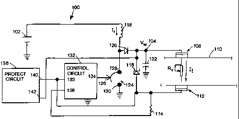
19 Fig. 4 illustrates a schematic diagram of a voltage boosting
electrotransport circuit 100 with an adjustable boost multiple that is
adjusted
21 according to the sensed therapeutic load current level in accordance with
the
22 present invention. This permits more efficient use of batteries and results
23 in significant size and cost savings when compared to the just-described
24 prior art. The circuit 100 inciudes a power source in the form of a battery
102,
and a voltage controlled electrical junction 104 electrically connected to an
26 electrode assembly 108. The electrode assembly 108 is attached to one
27 region of an animal body 110 by conventional means such as adhesive, 28
straps, belts or the like. The animal body surface is shown schematically
29 as a variable resistance load, Rv, to indicate the variation of load
resistance
typical of the skin when applying electric current li therethrough.
CA 02217711 1997-10-07
WO 96/38199 PCT/US96/08258
13
1 An electrode assembly 112 is similarly attached to another region of
2 the animal body 110. The electrode assembly 112 is connected to a series
3 current sensing resistor 114. The electrodes 108, 112, the body surface 110
4 and sense resistor 114 form a load current path for conducting the load
current, I,. The electrode assemblies 108, 112 are equivalent to the
6 electrode/reservoir combinations 22, 26 and 24, 28 shown in Fig. 2.
7 At least one of the electrode assemblies 108, 112 contains a therapeutic
8 agent (e.g., a drug salt) in a form (e.g., an aqueous solution) suitable for
9 electrotransport delivery into the animal body 110.
An energy storage inductor 118 is connected between battery 102 and
11 the anode of rectifying diode 120. The cathode of diode 120 is connected to
12 the voltage controlled electrical junction 104. A filter capacitor 122 is
13 connected between the junction 104 and system ground.
14 A controlled switch 124, having a control input 126, has one terminal
128 connected to the junction of the anode of diode 120 and the inductor 118
16 and another terminal 130 connected to system ground. The control input 126
17 can alternately open and close the switch 124 creating a low resistance
18 connection between the terminals 128 and 130 thereby connecting or
19 disconnecting the inductor 118 through a low resistance path to system
ground. The switch 124 may be an electronic switch device such as a bipolar
21 or FET transistor.
22 A control circuit 132 has a control output 134 connected to switch
23 control input 126. The control circuit 132 includes a feedback input 133
for
24 controlling the control output 126 and a switch input 136.
The operation of the adjustable voltage boost circuit 100 can be
26 understood with reference to Fig. 5. After initiation of the circuit 100,
27 for example, by means of a push button switch 12 illustrated in Fig. 1,
28 the control circuit 132 is adapted to first connect the input 136 to system
29 ground. This enables the sense resistor 114 to begin conducting load
current,
I1, from the load 110.
CA 02217711 1997-10-07
WO 96/38199 PCT/US96/08258
14
1 The control circuit 132 is configured to then toggle the control output
2 134 so that the switch 124 connects the one end of the inductor 118 to
3 ground for a period of time T1. During the time T1, the inductor current Ii,
4 driven by the battery 102, increases to a maximum value, IP.
At the end of time T1, the control circuit 132 is adapted to change
6 output 134 to toggle switch input 126 again which opens the switch 124 for a
7 time period, T2. During T2, the inductor current, I;, will not flow toward
8 ground, but is forced to conduct through the diode 120 into the electrical
9 junction 104. The filter capacitor 122 provides a low impedance path for the
instantaneous current, I;, which then decays toward zero during the time,
11 T2, as the voltage at electrical junction 104 is boosted by the charging of
the
12 capacitor 122.
13 During the time Tl, the inductor 118 stores energy by charging with the
14 current, I. During the period T2, the inductor 118 discharges energy into
the
filter capacitor 122 through the diode 120. The inductor 118 thereby
16 transfers energy from the battery 102 into the capacitor 122 with low loss,
17 limited only by the diode 120 drop and the negligible series resistance of
the
18 inductor 118, battery 102 and the electrical connections. Thus, the energy
19 source for load current Ii is not directly the battery 102 but rather
either the
capacitor 122 (i.e., during time T1) or a combination of the capacitor 122 and
21 inductor 118 (i.e., during time T2).
22 The control circuit 132 is adapted to repeat the T1, T2 cycle indefinitely
23 or when stopped as described below. The voltage, VW, at the junction 104 is
24 thereby boosted to a adjustable multiple of the battery 102 voltage
depending
on the values of the time periods T1 and T2. The boost multiple thus can be
26 adjusted by adjusting the values of T1 and T2.
27 Dotted lines in Fig. 5 indicate missing or delayed pulses as controlled
28 by the control circuit 132. This may occur when pulses are not necessary to
29 replace charge depleted from the capacitor 122, for example, when the
therapeutic current, Ii, demanded is relatively low. The dotted lines in Fig.
5
CA 02217711 1997-10-07
W O 96/38199 PCT/US96/08258
1 indicate that the boost multiple control means may be by pulse width
2 modulation (PWM), pulse frequency modulation (PFM), pulse skipping,
3 or some combination thereof.
4 The adjustable working voltage, VW, causes the load current, I,, to flow
5 through the animal body load 110, through the sense resistor 114 and into
the
6 switch input 136, to ground.
7 The feedback input 133 senses the voltage across the sense resistor
8 114 caused by the load current, li. The control circuit 132 is adapted to
9 respond to the feedback input 133 to boost the working voltage, VW, by
10 adjusting the time periods, T1 and T2. This is accomplished by comparing
11 the voltage sensed at input 133 with a set reference voltage within control
12 circuit 132. If the voltage sensed at input 133 is less than the reference
13 voltage, then control circuit 132 opens and closes switch 124 at a high
14 frequency until VW is boosted to the appropriate level. In general, the
longer
15 switch 124 is closed (i.e., the longer is T1), the greater the voltage
which is
16 developed in inductor 118 and the greater the boost multiple. The battery
17 102 voltage can be boosted by reason of the inductor 118. The voltage
18 developed in the inductor 118 is equal to the inductance value (L)
multiplied
19 by the rate at which current flows through the inductor:
21 Vind = L (dli/dt).
22 Thus, out of inductor 118 comes a higher voltage (which voltage is
23 determined in part by the inductance value of inductor 118 and in part by
the
24 rate of current flow through inductor 118 which is controlled by the values
of
T1 and T2) at a lower current since the power into inductor 118 must equal
26 the power out of inductor 118.
27 The control circuit 132 is additionally adapted such that, in combination
28 with the values of the inductor 118, the value of the load resistance 110
and
29 the capacitance value of the capacitor 122, the time periods, TI, T2, are
arranged in response to the voltage at the feedback input 133 such that filter
CA 02217711 1997-10-07
WO 96/38199 PCT/US96/08258
16
1 capacitor 122 smooths and adjusts the voltage VHõ to provide a load current,
2 Ii, of an essentially constant (DC) current of predetermined value.
3 The electrode assemblies 108 and 112, and thus the animal body 110,
4 are not exposed to high peak voltages as in the prior art, but instead
experience only the minimum, voltage value sufficient to drive the desired
6 load current li.
7 The time periods T1 and T2 are adjusted by the control circuit 132 to
8 boost Võ, to the minimum absolute value to provide the load current li to
9 maintain a desired predetermined value. If the resistance of the load 110 is
too high to allow the predetermined value of I, to be attained without having
11 V,, exceed a safe level, a voltage limiting device, such as a zener diode
116
12 connected across the electrode assemblies 108 and 112, limits the voltage
13 applied to load 110. A typical safe maximum limiting value for V, is about
14 24 volts. Other values of limiting voltage can be achieved by zener diodes
116 having different breakdown voltages, or by using other protection means
16 as described further below.
17 Once the resistance of the load 110 decreases sufficiently to allow the
18 load current, I,, to reach the desired predetermined level at the maximum
safe
19 voltage, the control circuit 132 will respond to the feedback at feedback
input
133 and will adjust T1 and T2 to boost V, to a multiple just sufficient to
21 maintain the current at the predetermined level independent of further
22 resistance decreases.
23 The working voltage, VW, at the controlled electrical junction 104 is
24 thus boosted to a boost multiple of the battery 102 voltage just sufficient
to
maintain the load current, I1, at the predetermined value as long as the load
26 voltage is less than the limiting voltage set by the zener diode 116.
27 The low loss transfer of energy from the battery 102 to the load 110
28 and capacitor 122 maximizes the useful life of the battery 102, for a given
29 battery capacity. This allows smaller batteries to be used for a given
CA 02217711 1997-10-07. ,` f._J~V/J J t=
2384 CIP 1
17
1 therapeutic regimen, or extends the lifetime of therapeutic treatment at a
given
2 cost.
3 The predetermined current )t applied across load 110 may be constant or
4 varying with time. In either event, the control circuit 132 is provided with
means for establishing a predetermined current-time profile to be applied.
This
6 may be accomplished by means well known in the art, such as a differential
7 comparator having one input connected to the sense resistor 114, a constant
8 reference voltage connected to the other input, or having the other input
9 connected to the output of a D to A converter driven by a clocked ROM having
a pre-programmed pat:ern (not shown in Fig. 4).
11 The circuit 100 may also be provided with a protection circuit 138. The
12 protection circuit 138 has high impedance and low impedance checking
13 functions and inciudes an input 140 which senses the voltage drop across
load
14 1 10 and compares the sensed voltage drop against a preset minimum limit
therefor, Circuit 138 also includes an input 142 which senses the current ~
16 applied through load 110 and compares the sensed current against a preset
17 maximum limit therefor. ProteGtion circuits offering impedance checking and
18 shut ctown protection are well known in the art. See, for example the
'19 protection circuits shown in Fig. 1 of Jacobsen et al US Patent 4,141,359.
The protection circuit 138 monitors the resistance of the load 110 by
21 the voltage input 140 and the current input 142 and shuts down the voltage
22 boosting function of the circuit 100 when the resistance of the load 110
23 exceeds a predetermined upper limit or decreases below a predetermined
lower
24 limit. Incorporation of the protection and shutdown circuit 138, of the
type
cfescribe in US Patent 4,141,359, into the booster circuit 100 is within the
26 capability of a person having ordinary skill in the electrical arts.
Ak-IEND-FD SHi:EC
CA 02217711 1997-10-07
WO 96/38199 PCTIUS96/08258
18
1 In use, the electrode assemblies 108 and 112 are attached to the
2 skin surface 110 by conventional means, and the therapeutic current is
3 initiated, by a switch means (not shown) such as switch 12 shown in Fig. 1.
4 The control circuit 132 begins controlling the on and off switching of
switch 124. Repetitive pulses of inductor current, I;, are alternately
6 charged during the on time periods, T1, through the switch 124 to ground
7 and discharged during the off time periods, T2 into the capacitor 122.
8 These pulses of inductor current Ii cause the voltage, V,, to be multiplied
by
9 an adjustable boost multiple by adjusting the on and off times T1, T2 until
the
signal to feedback input 133 indicates the load current I, is in regulation.
11 Fig. 6 shows another adjustable boost circuit 200 in accordance
12 with this invention. The circuit 200 includes a battery 202, an inductor
204,
13 a diode 206, a voltage controlled electrical junction 207, a low resistance
filter
14 capacitor 208, and electrode assemblies 210, 212 which are attached by
conventional means to spaced apart regions of animal body 213. The animal
16 body 213 is represented schematically as a variable load resistance Rõ to
17 emphasize the fact that the resistance of the load 213 does vary with time
18 and current.
19 At least one of the electrode assemblies 210, 212 contains a
therapeutic agent in a form suitable for electrotransport delivery into the
21 animal body 213.
22 The circuit 200 includes an N-channel field effect transistor (FET)
23 switch 218, for switching inductor current I;, an inductor current sense
24 resistor 220, and a load current sense resistor 214. The circuit also
includes
a high efficiency, adjustable DC-DC step up controller 216. A preferred
26 controller 216 is the Maxim MAX773 made by Maxim Integrated Products,
27 Inc. of Sunnyvale, CA.
28 Fig. 6 shows a simplified schematic of the MAX773 controller 216
29 which is sufficient for purposes of the present invention. A more detailed
schematic of the MAX773 controller can be found in the MAX773 data
CA 02217711 1997-10-07
W O 96/38199 PCT/US96/08258
19
1 sheet 19-0201;Rev 0; 11;93, which is available from the manufacturer.
2 The controller 216 is an integrated circuit having internal components
3 connected by conductive traces formed during the integrated circuit
4 manufacturing process. External pins are provided for electrical connection
to
external components by conventional printed circuit means such as plated or
6 deposited copper or other conductors deposited and formed on insulating
7 substrates. Reference to electrical connections in the description herein
are
8 understood to be internal or external as shown in Fig. 6. References to the
9 components of the MAX773 controller circuit are illustrative for the
purposes
of describing the function of circuit 216. Unlike traditional pulse frequency
11 (PFM) converters, which use an error voltage from a voltage divider circuit
to
12 control the output voltage of the converter to a constant value, controller
216
13 is connected to use the sense resistor 214 to generate an error voltage to
14 control the average load current I,. The MAX773 controller also operates
with high frequencies, (up to 300 kHz) allowing the use of small external
16 components. The controller 216 includes a reference voltage pin 256, a
17 ground pin 258, a grounding switch input 260, a low level threshold input
262,
18 a feed back input 264, a shut down input 266, a current sense input 268,
and
19 a power bus input 270.
Controller 216 also includes a first two-input comparator 230 having an
21 output 231, a second two-input comparator 232 having an output 233, a first
22 reference voltage 242, a second (e.g., 1.5 volt) reference voltage 244, a
third
23 two-input comparator 246 having an output 247, a PFM/PWM driver circuit
24 240 having a switch control output 252 and a switch control output 254, and
a
second N-channel FET switch 250.
26 Operation of the circuit 200 can be understood by reference to
27 Figs. 6 and 7. The circuit 200 uses the controller 216 in a novel way to
28 provide a high efficiency conversion of energy from the battery 202 into an
29 adjustably boosted voltage V, at the voltage controlled electrical junction
207
and simultaneously controlling the load current I,.
CA 02217711 1997-10-07
WO 96/38199 PCT/US96/08258
1 With reference to Fig. 6, in accordance with this invention, a portion of
2 the load current I, is fed back to the feed back input 264. One terminal of
3 sense resistor 214 is connected to the feed back input 264. This same
4 terminal of resistor 214 is also connected to the electrode assembly 212 for
5 receiving the load current I. The other terminal of resistor 214 is
connected
6 to the input 260 of controller 216. The input 260 internally connects to the
7 drain of the N-channel switch 250. The source of switch 250 connects to
8 system ground. The gate of switch 250 connects to the output 247 of
9 comparator 246. The inverting input of comparator 246 connects to the
10 input pin 262. The input pin 262 is connected to system ground. The non-
11 inverting input of comparator 246 is connected to the reference voltage
244.
12 The reference voltage 244 also connects to the reference voltage pin 256.
13 The comparator 246 is driven such that output 247 is always high.
14 Switch 250 will therefore be driven to conduct the pin 260 to ground,
15 sinking the load current li to ground through the sense resistor 214.
16 The input 264 connects to the inverting input of comparator 232.
17 The non-inverting input of comparator 232 is connected to the reference
18 voltage 244. The output 233 of comparator 232 is connected to the
19 PFM/PWM driver circuit 240.
20 The output 231 of comparator 230 is connected to the PFM/PWM
21 driver circuit 240. The inverting input of comparator 230 is connected to
the
22 reference voltage 242. The non-inverting input of comparator 230 connects
23 to the current sense input 268. Input 268 is connected to one terminal of
24 inductor current sense resistor 220. The other terminal of resistor 220
connects to system ground. The ground pin 258 of the controller 216 is
26 also connected to system ground.
27 One output of the PFM/PWM driver circuit 240 connects to the
28 output 252. The input 270 is connected to one terminal of the battery 202.
29 The other terminal of the battery 202 is connected to system ground.
One output of the PFM/PWM driver circuit 240 connects output 254.
CA 02217711 1997-10-07
W O 96/38199 PCT/US96/08258
21
1 The outputs 252 and 254 are both connected to the gate of the external
2 N-channel switch 218. The drain of the switch 218 is connected to a joint
3 connection of one end of the energy storage inductor 204 and the anode of
4 rectifying diode 206. The source of the switch 218 is connected to the one
terminal of the inductor current sense resistor 220 which is connected to the
6 current sense input 268.
7 The other terminal of the inductor 204 is connected to the power
8 bus input 270 and to the terminal of the battery 202. A filter capacitor 276
is
9 connected between the input 270 and ground. A filter capacitor 278 is
connected between the voltage pin 256 and ground. The filter capacitors 276
11 and 278 have low dynamic impedance at the pulse frequencies of interest.
12 The cathode of diode 206 is connected to an electrical junction 207.
13 The junction 207 is also connected to one terminal of a filter capacitor
208,
14 the cathode of a zener diode 280 and the electrode assembly 210.
The anode of the zener diode 280 and the other terminal of capacitor 208
16 are connected to ground. The junction 207 completes the circuit 200 which
17 boosts the working voltage, VW, at the junction 207 by an adjustable
multiple
18 of the voltage of the power source, i.e., battery 202.
19 The zener diode 280 provides a means to limit the peak voltage across
the electrode assemblies 210 and 212 and thus the maximum voltage
21 experienced by the animal body load 213.
22 With reference to Figs. 6 and 7, the operation of the adjustable voltage
23 boost multiple circuit 200 can be understood. When power is applied by the
24 battery 202 to input 270 and the input signal 266 is of the correct logic
level,
the controller 216 begins operating. Since input 262 is held low,
26 and the non-inverting input of comparator 247 is at, e.g., 1.5 volts,
27 from reference voltage 244, the output of the comparator 246 will be high.
28 With a high voltage on the gate of the switch 250 the input 260 will be
driven
29 to ground by the drain of switch 250. This enables the resistor 214 to
receive
load current li from the electrode assembly 212.
CA 02217711 1997-10-07
WO 96/38199 PCT/US96/08258
22
1 As with traditional PFM converters, the switch 218 is not turned on until
2 the voltage comparator 232 senses the output current is out of regulation.
3 However, unlike traditional PFM converters, the MAX773 uses the
4 combination of the peak inductor current limit sense resistor 220, reference
voltage 242 and comparator 230 along with the maximum switch on-time
6 and minimum switch off-time generated by the PFM/PWM driver circuit 240;
7 there is no oscillator. The typical maximum switch on-time, T1, is 16 micro
8 seconds. The typical minimum switch off-time, T2, is 2.3 micro seconds.
s Once off, the minimum off-time holds the switch 218 off for time T2.
After this minimum time, the switch 218 either (1) stays off if the output
11 current li is in regulation, or (2) turns on again if the output current li
is out
12 of regulation.
13 While the switch 218 is off, the inductor current li flows through the
14 diode 206 into the capacitor 208 at junction 207, replenishing any charge
drawn off by the load 213. It can be seen that this method of switching the
16 charging current Ii provides an adjustable boost multiple of the battery
202
17 voltage to a working voltage V, at the junction 207, just sufficient to
supply
18 the desired constant current I,. The peak voltage delivered by the inductor
19 204, will be just that required to overcome the diode drop of the diode 206
and the working voltage VW and thus minimizes energy loss from the
21 battery 202.
22 The controller 216 circuitry allows the circuit 200 to operate in
23 continuous-conduction mode (CCM) while maintaining high efficiency with
24 heavy loads. When the power switch 218 is turned on, it stays on until
either
(1) the maximum on-time turns it off (typically 16 microseconds later), or (2)
26 the inductor current I; reaches the peak current limit IP set by the
inductor
27 current limit resistor 220, the reference voltage 242 and comparator 230.
28 In this event, the on time will be less than the maximum on time, T1.
Limiting
CA 02217711 1997-10-07
WO 96/38199 PCT/US96/08258
23
1 the peak inductor current, to a predetermined maximum, Ip, avoids saturating
2 the inductor 204 and allows the use of smaller inductor values, thus smaller
3 components.
4 If the average load current I, is below the desired value as set by the
value V,ef of reference voltage 244 and the resistance value Rs of sense
6 resistor 214 through the relation
7 Vref > lt = Rs
8 then the PFM/PWM driver circuit 240 will automatically adjust the on time T1
9 and the off time T2 and alternately turn the switch 218 on and off until the
load current li is in regulation.
11 Operation of the adjustable boost multiple circuit 200 may be initiated
12 by connecting the shut down input 266 to a logic high level by switch
means,
13 such as switch 12 shown in Fig. 1. When shut down input 266 is high, the
14 MAX773 circuit enters a shut down mode. In this mode the internal biasing
circuitry is turned off (including the reference), switch 250 enters a high
16 impedance state and the working voltage V,N falls to a diode drop below the
17 battery 202 voltage (due to the DC path through the inductor 204 from the
18 battery 202 to the electrode assembly 210). The supply current from the
19 battery 202 becomes equal to VW/ I,. However, no current path is available
with the high impedance state of switch 250 and the load current I, is zero.
21 In alternate embodiments of this invention, the current li may be
22 programmed to follow a predetermined profile by programming the value of
23 the load current sense resistor 214. The resistor 214 value may be
24 programmed by switching additional resistors in parallel or series with the
load current I,. Such switching control means are well known in the art.
26 Fig. 8 shows a schematic diagram of an electrotransport device 300
27 having an alternative voltage boosting circuit. The device 300, unlike
devices
28 10 and 10' shown in Figs. 1 and 2, has a reusable controller 302 which is
29 adapted to be separably coupled to a plurality of single-use, preferably
disposable, drug units 304, one at a time in succession. The disposable
CA 02217711 1997-10-07
WO 96/38199 PCT/US96/08258
24
1 drug unit 304 is attached to an animal (e.g., human) body surface, such as
2 the skin 306, which is schematically illustrated in Fig. 8 as a resistor
having
3 a variable load resistance R1. Drug Unit 304 has a pair of electrodes
4 (i.e., an anodic electrode 308 and a cathodic electrode 310), at least one
of which contains a therapeutic agent to be delivered through the skin 306
6 by electrotransport. The drug unit 304 and the controller 302 may be
7 mechanically and electrically coupled by a pair of metal snap
8 connectors 336,338. Thus, electrotransport load current II is supplied
9 to the drug unit 304 and the patient's body via the conductive snap
connectors 336,338.
11 The controller 302 includes two circuit portions; a voltage boosting
12 circuit 312 for boosting a supply voltage V+ provided by the power source
13 (e.g., a battery) 318, to a working voltage, V,,,, and a low load voltage
current
14 sinking circuit 314. When the voltage, VW, at the load resistance R1 is
high,
that is, when Vw is greater than V+, minus diode voltage, Vd, (dropped across
16 series diode 315), the voltage boost circuit 312 provides power to the load
17 306 through inductor 320 and diode 315 as described in more detail
18 hereinafter.
19 When the load resistance R1 decreases to a low value, such that
[(II = R1 ) i' Vref] < (V+ - Vd),
21 the control of load current II shifts to the current sinking circuit 314
which
22 allows the controller 302 to operate at lower skin resistance (R1) with
23 improved efficiency compared to the circuits described in Figs 4 and 6.
24 Operation of the voltage boosting 312 circuit in cooperation with the
current sinking circuit 314 can be explained in combination with the use of an
26 exemplary PFM/PWM controller 322. A representative example of such a
27 controller 322 is the MAX771 available from Maxim Integrated Products, Inc.
28 of Sunnyvale, CA although other PFM/PWM switching controllers available in
29 the art, can also be used.
CA 02217711 1997-10-07
WO 96/38199 PCT/US96/08258
1 The power source 318 is typically a battery having a plus and minus
2 terminal. The plus terminal, V+, is connected to power input pin 323 on the
3 circuit 322 and to one terminal of the inductor 320. The minus terminal of
the
4 battery 318 is connected to system ground.
5 The other terminal of the inductor 320 is connected to the junction of
6 the anode of the diode 315 and the drain 324 of an n-channel switch 326.
7 The source of switch 326 is connected to one terminal of a peak
8 current sense resistor 328. The other terminal of the resistor 328 is
9 connected to system ground. The gate of switch 326 is connected to a switch
10 control output 330 of circuit 322.
11 A sense input 332 of circuit 322 is also connected to the junction
12 between the source of switch 326 and one terminal of peak current
13 sense resistor 328.
14 The cathode of diode 315 is connected to one terminal of a filter
15 capacitor 334. The other terminal of capacitor 334 connects to system
16 ground. The junction of capacitor 334 and diode 315 cathode are connected
17 through snap connector 336 to the anodic electrode 308 in contact with the
18 patient's skin 306. Cathodic electrode 310 is also in contact with the
patient's
19 skin 306 and is connected to snap connector 338.
20 Snap connector 338 is connected to the drain of a second n-channel
21 transistor 340 having a gate and source. The transistor 340 drain and
source
22 are connected in series forming part of the current sinking circuit 314
which
23 receives the load current 11. The source of transistor 340 connects to one
24 terminal of a first load current source resistor 342 having a resistance
value
25 R2. The other terminal of the resistor 342 is joined to a second load
current
26 source resistor 344 having a resistance value R3. The other terminal of the
27 resistor 344 is connected to system ground.
CA 02217711 1997-10-07
WO 96/38199 PCTIUS96/08258
26
1 The junction of the resistor 342 and resistor 344 are joined to the
2 inverting input of a high impedance, two-input differential op-amp 346,
3 having a high voltage gain, Av. The output of the op-amp 346 connects
4 to the gate of the transistor 340. The non-inverting input of the op-amp 346
connects to a reference voltage output 348 (Vref) of the circuit 322.
6 The junction of the transistor 340 source and the one terminal of
7 resistor 342 connect to a feedback input 350 (FB) of the circuit 322 to
provide
8 control of the load current li through the patient.
9 Operation of the circuit 302 can be considered in two regimes: (i) when
skin resistance R, is high, and (ii) when skin resistance R, is low. Operation
11 in regime (i) is as follows. When the skin resistance R, is high, such that
12 [(1I - R1 ) + Vref] > (V+ - Ud),
13 the current li is controlled by the circuit 322. There is feedback of the
voltage
14 at the one terminal of the load current sense resistor 342 connected to the
input 350. The circuit 322 compares the voltage at the input 350 to the
16 voltage at the Vref input 348 and adjusts the switching rate and pulse
width of
17 the output 330 to alternately charge inductor 320 with current li, and
18 discharge into capacitor 334 through diode 315 until the feedback voltage
at
19 input 350 (given by load current li times the sum of (R2+R3), i.e., the sum
of
the resistance values of feedback resistors 342 and 344) is equal to the Vret
21 voltage 348.
22 The value of resistors 342 and 344, the gain Av of the op-amp 346,
23 and the value of Vref at output 348 are selected such that, at the desired
load
24 current li, the difference between the voltage Vref at output 348 and the
feedback voltage at the junction of resistor 342 and resistor 344 to the
26 inverting input of the op-amp 346 will cause the output of op-amp 346 to
drive
27 the gate of transistor switch 340 sufficiently so that it is full on.
CA 02217711 1997-10-07
'WO 96/38199 PCTIUS96/08258
27
1 A portion of the feedback voltage across resistors 342, 344 is fed back
2 to the inverting input of the op-amp 346. The ratio of the resistance values
3 R2 : (R2+R3) and the gain Av of the op-amp 346 is selected such that the
4 output of op-amp 346 drives the transistor switch 340 into a low impedance
state so that it presents essentially no resistance relative to resistor 344.
6 Therefore, when the average value of li is too low, that is, when li times
7 (R3 + R2) is lower than Vref 348, the feedback input 350, in combination
with
8 the peak current sense resistor 328 causes the switch output 330 to toggle
at
s a rate and pulse width sufficient to charge and discharge the inductor 320
with current II such that the average current li through the skin 306 will be
in
11 regulation, without saturating the inductor 320.
12 The circuit 322 acts to limit li to a peak current such that inductor 320
13 will not saturate by sensing the peak voltage across resistor 328 and
limiting
14 the on pulse width of the transistor 326.
Operation in regime (ii) on the other hand is controlled by the current
16 sinking circuit 314, as follows. As the patient's skin resistance R1 tends
17 toward a low value, such that
18 [(II - R1)+Vref] < (V+-Ud)+
19 the load current li will not be limited by the skin resistance R1 and will
tend to
increase.
21 In the limit, as R, approaches zero, li will increase, limited only by the
22 voltage V+ divided by the series resistance of resistors 342, 344 and the
23 resistance of the transistor 340.
24 An increase in Ii will drive the voltage at the source of the transistor
340 positive until the feedback input 350 causes the boost circuit to begin to
26 lose control over the load current li, as the circuit 322 will not have to
toggle
27 the switch 326 to maintain load current li.
CA 02217711 1997-10-07
WO 96/38199 PCT/US96/08258
28
1 In the circuit of Fig. 8, the resistor 342 and 344 are selected so that the
2 ratio of R3 : (R2+R3) is sufficiently close to one, ie, the resistance value
R2 is
3 much less than the resistance value R3 (eg, R2 = 3 ohms;
4 R3 = 1.5 k-ohms).. In regime (ii), as Ii increases and the voltage across
resistor R3 rises, the voltage difference at the inputs to the op-amp 346
6 decrease enough to cause the output of the
7 op-amp 346 to lower the voltage at the gate of transistor 340.
8 Transistor 340 then comes out of saturation and begins to present a
9 varying impedance in series with R2 and R3. The transistor impedance will
vary, being controlled by the op-amp 346 and the inputs, Vref and the portion
11 of the negative feedback voltage (ie, the feedback voltage to op-amp 346
12 which feedback voltage is equal to the load current times resistance value
R3,
13 ie, Ii = R3). The variation of the additional impedance provided by
transistor
14 340 prevents the tendency for Ii to continue to increase.
The gain Av of op-amp 346 and the ratio R3 : (R2+R3) are selected
16 such that the difference between the current Ii in regime (i) and regime
(ii)
17 are sufficiently close. An op-amp with a gain greater than 1000 and
resistor
18 R2 of 3 ohms, resistor R3 of 1.5 k-ohms will differ by much less than 5%.
19 Previously, this situation was overcome with additional control logic
(i.e., a microprocessor), resistors and switches. The logic would detect a
21 "below supply voltage" situation and switch in a resistor in series with
the
22 load 306, forcing the boost circuit 312 back on to reestablish current
control.
23 The addition of a microprocessor and other components add cost and
24 additional current drain to operate, reducing efficiency. It is also less
efficient
to run the boost circuit 312 continuously, if it is not needed. This becomes
26 even more an issue when the supply voltage is larger.
CA 02217711 1997-10-07
WO 96/38199 PCT/US96/08258
29
1 The current sinking circuit 314 in combination with the boost circuit 312
2 provides a simple, low cost, electrically efficient and effective means for
3 controlling the therapeutic current li to a reasonable constant value over a
4 very wide range of skin resistance R, .
The additional impedance presented by the transistor 340 in regime (ii)
6 could be provided by other active devices, such as a p-channel transistor or
a
7 pnp or npn bipolar transistor, or the like. Current sensing could be
provided
8 by a Hall effect sensor or other magnetic sensing devices such as a switched
9 current sampling transformer. Suitable feedback amplification could also be
provided by discrete transistors and resistor, capacitor circuit assembled
into
11 a differential amplifier, which is well within the capability of those
skilled in
12 the art.
13 Although this invention has been described with some particularity in
14 respect to embodiments thereof which, taken together, comprise the best
mode
known to the inventors for carrying out their invention, many changes could be
16 made, and many alternative embodiments could thus be derived without
17 departing from the scope of the invention. Consequently, the scope of the
18 invention is to be determined only from the following claims.