Note: Descriptions are shown in the official language in which they were submitted.
. ~ _ ~ CA 02217868 1997-10-09
F~LE, ~,'~ Tl~'~r~ rh~
F~ TRAN~L~TION
[10191/521]
FREQUENCY ERROR DETECTOR
Background of the invention
The present invention concerns a frequency error detector that
determines the ~requency deviation between a carrier frequency
generated in a receiver and the carrier ~requency of a
received signal, wherein there is a first differential power
meter that forms the power difference between spectral
components of the spectrum of the received signal that are
symmetrical with the receiver carrier ~requency.
Frequency error detectors are used for automatic frequency
control (AFC) in control 1QOPS that are in radio transmission
receivers, for example, for coherently modulated signals
(e.g., quad amplitude modulation, QAM) to adjust the carrier
~requency of the receiver to the carrier frequency o~ the
transmitter, i.e., the carrier frequency of the received
signal. In addition, these receivers for coherently modulated
signals often have another closed loop for carrier phase
synchronization which is capable of synchronization in the
case o~ relatively small ~requency deviations. The ~requency
error allowed in synchronization of the carrier phase is
called the lock-in range. Since the transmission carrier
frequency is not known at the start o~ a transmission or after
a system failure, the receiver must be capable of reliably
estimating this frequency. The accuracy of this estimation
must be within the lock-in range of the carrier phase
synchronization. The size of this lock-in range depends on
several system parameters of the broadcast system. Narrow-
band broadcast systems with a high number of modulation levels
have a smaller lock-in range, but broad-band systems with
fewer modulation levels have a larger lock-in range.
A frequency error detector of the type describe~ in the
preamble is a sui~able device that synchronizes the carrier
~requency of the receiver at the transmission carrier
frequency. It measures the di~ferential power o~ the received
.' CA 02217868 1997-10-09
signal spectrum symmetrically with the center of the band. An
error signal generated in this way will disappear at the
correct carrier frequency in the receiver. A quadricorrelator
such as that known from German Patent No. 37 07 7~2 C2 is one
such frequency error detector. This quadricorrelator reacts
very sensitively to signal distortions; i.e., it supplies
false information about the frequency deviation when the
received signal spectrum is skewed because of channel
distortion. Straight-line broadcast systems usually have
great channel distortion. Therefore, the background art
frequency error detector would not be suitable for a receiver
in a transmission system where channel distortion is expected.
The object of this invention is therefore to provide a
frequency error detector of the type defined in the preamble
that will supply the most accurate possible information about
the deviation in the carrier frequency in the receiver in
comparison with the transmitted carrier frequency regardless
of channel distortions.
Advantages of the invention
According to the features of Claim 1, the object formulated
here is achieved by the fact that in addition to the first
differential power meter, a second differential power meter is
provided to form the power dif~erence between spectral
components that are symmetrical with the received carrier
frequency and belong to the spectrum formed by undersampling
of the received signal, and a summation circuit is provided
that generates, from the output signals of the two
differential power meters, a summation signal that provides
information on the frequency deviation. Useful refinements of
this invention are derived from the subclaims.
Description of an embodiment
The invention is explained in greater detail on the basis of
-
. ~ CA 02217868 1997-10-09
one embodiment illustrated in the drawing, where:
Figure 1 shows a block schematic of a receiver,
Figure 2 shows a frequency error detector used in the
receiver,
Figures 3, 3a, 3b show signal spectra belonging to a first
differential power meter, and
Figures 4, 4a, 4b show signal spectra belonging to a second
differential power meter.
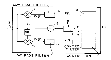
Figure 1 shows a receiver designed as a phase-locking loop for
coherently modulated signals, e.g., QAM signals. This phase-
locking loop has two mixers 1 and 2 that convert the signal
they receive over input line 3 into two baseband signals Xl(t)
and Yl(t). Low-pass filters 4 and 5 suppress unwanted signal
components in the two baseband signals Xl(t) and Yl(t) and
thus generate two signals X(t) and Y(t). Both signals X(t)
and Y(t) are sent to a contact unit 6 with a frequency error
detector that analyzes signals X(t) and Y(t) in a manner to be
described in greater detail below and derives from them a
frequency correction signal S that is delivered to a control
filter 8 over output line 7. This control filter 8 has the
function of smoothing the frequency correction signal S and
routing it to a controllable oscillator 9 that generates a
carrier signal for mixers 1 and 2, with the carrier signal for
mixer 2 being phase rotated by 90~. Frequency error detector
6 needs a sampling pulse that corresponds to the half symbol
pulse T/2 of the received signal for sampling signal
components X(t) and Y(t), which are phase shifted by 90~.
Signal components X(t) and Y(t) reproduce the respective
received signal value exactly only when the carrier generated
by oscillator 9 is ~requency-synchronized with the carrier of
the received signal.
As explained in the preamble, the frequency error detector
should provide information on the frequency deviation between
the carrier ~requency of oscillator 9 and the carrier
. ' CA 02217868 1997-10-09
frequency of the received signal as independently of any
channel distortion as possible. This requirement is met by a
frequency error detector consisting of two differential power
meters, e.g., quadricorrelators. A differential power meter
is known to form the power difference between spectral
components of the received signal spectrum that are
symmetrical with the receiver carrier frequency. The first
differential power meter receives a received signal spectrum
that is generated by sampling twice per symbol pulse of the
received signal (maintaining the Nyquist criterion). Figure 3
shows such a spectrum, which is repeated periodically without
overlap. The spectrum shown in Figure 3 is ideally
symmetrical with the receiver carrier frequency TE; i.e.,
there is no frequency deviation between the receiver carrier
~requency TE and the carrier frequency of the received signal.
The pass bands (shaded areas) of two band-pass filters of the
differential power meter are also symmetrical with the
receiver carrier frequency TE in proximity to the Nyquist
edges of the received signal spectrum. The spectral
components selected by the two band-pass filters are equal in
size in this case, so the difference between the powers of
these spectral components yields a value of zero. The second
differential power meter processes a spectrum (shown folded
over in Figure 4) which is formed by undersampling (failure to
uphold the Nyquist criterion). These mutually overlapping
spectra are obtained when the received signal is sampled only
once per symbol pulse T. The pass bands of the band-pass
filters of this second differential power meter are now closer
to the carrier frequency TE of the received signal, i.e., at a
greater distance from the Nyquist edges of the spectrum.
As explained in greater detail with reference to Figures 3a,
3b and 4a, 4b, the output signal of the first differential
power meter shows a dependence on both a frequency shift and a
channel distortion, and the output signal of the second
differential power meter shows almost no dependence on a
frequency deviation, but instead shows a dependence only on
-
. ' CA 02217868 1997-10-09
skewing of the spectrum caused by channel distortion. The
second differential power meter could therefore also be called
a distortion detector.
Figure 3a shows a spectrum processed by the first differential
power meter, which does not have any frequency shift but is
skewed because of channel distortion. This illustration shows
clearly that the selected spectral components that are
symmetrical with the receiver carrier frequency TE have
different powers because of the skewing. The output signal of
the first differential power meter is thus dependent on
channel distortion. In addition, it is of course also
dependent on a shift ~f between the receiver carrier frequency
TE and the received signal carrier frequency TF, as
illustrated in Figure 3b. The solid line indicates a spectrum
without frequency shift and the dashed line indicates a
spectrum with the frequency shift ~f. The spectral components
selected by the first differential power meter at the Nyquist
edges of the spectrum shifted by ~f have different powers,
depending on the frequency shift ~f. To this extent, the
output signal of this first differential power meter contains
information about the frequency shift ~f.
Figure 4a shows a folded spectrum that has skewing caused by
channel distortion and is processed by the second differential
power meter. It can be seen here that the spectral components
selected to be symmetrical with the receiver carrier frequency
TE have different powers, the output signal of the second
differential power meter is also dependent upon channel
distortion. However, if there is a frequency shift ~f between
the receiver carrier frequency TE and carrier frequency TF of
the received signal, then the spectral components selected
from the shifted spectrum (dashed line) have the same power
levels. The power difference of the selected spectral
components is therefore zero, although there is a frequency
shift ~f. The output signal of the second differential power
meter thus shows a dependence only on channel distortion. The
CA 02217868 1997-10-09
output signal o~ the second di~erential power meter which
depends only on channel distortion can thus be used to
compensate for the dependence of the output signal o~ the
~irst di~ferential power meter on channel distortion, so that
ultimately a signal derived ~rom the superposition o~ the two
output signals depends only on the frequency deviation between
the receiver carrier frequency TE and the received signal
carrier ~requency TF. Such an error correction signal S
(Figure 1) would synchronize oscillator 9 at the correct
carrier frequency, regardless of channel distortion.
Figure 2 shows a simple example of a circuit where the two
differential power meters are combined. In this embodiment,
the dif~erential power meters each have the structure o~ a
quadricorrelator, which is known ~rom German Patent No.
37 07 762 C2, for example. The discrete-time signals xn and Yn
derived by sampling the in-phase signal component X(t) and the
quad signal component Y(t) of the received signal are applied
to two inputs of the frequency error detector. From these
discrete-time signals xn and Yn, a first quadricorrelator
derives, according to equation (1), a signal un having a
dependence on both frequency shift and channel distortion:
Un = Yn xn-l - XnYn~
Subscripts n and n-1 indicate the sampling times in the half
sampling pulse T/2. This equation (1) is implemented
according to Figure 2 with the help of two time-delay elements
lO and 11, which delay the discrete-time input signals xn and
Yn by one sampling pulse, and a first multiplier 12, which
generates product ynXn l, and a second multiplier which ~orms
product xnyn1. A subtracter 14 forms the dif~erence o~ the
output signals of the two multipliers 12 an 13 and ~inally
supplies signal un.
Output signal vn o~ the second di~ferential power meter for the
folded received signal spectrum results ~rom the relation of
.- ~ CA 02217868 1997-10-09
the discrete-time received signal values xn/ xn2 and Yn/ Yn-2
according to equation (2):
Yn Xn-2 ~ Xn Yn-2 n even
vn = { (2)
o n odd
Received signal values xn2 and Yn-2 at time n-2 are obtained by
additional time-delay elements 15 and 16, which are connected
in series with the first time-delay elements 10 and 11. A
multiplier 17 generates the product of received signal values
ynxn2, and a multiplier 18 generates the product of received
signal values xnyn2. The difference between the two products
according to equation (2) is generated by a subtracter 19.
Time-delay element 20, which is connected to the output of
subtracter 19, works with symbol pulse l/T, so it selects only
every second value out of the differential signal. This
undersampling yields the folded spectrum according to Figures
4, 4a, 4b as described above. Output signal vn of time-delay
element 20 shows the desired dependence exclusively on channel
distortion. By combining signal vn/ which depends only on
channel distortion, and signal un, which depends on both
frequency deviation and channel distortion, a signal is
obtained in which the e~ects of channel distortion are
mutually compensated and which ultimately depends only on the
frequency deviation between the receiver carrier and the
received signal carrier. To optimize compensation of channel
distortion, it is expedient to weight the two signals un and vn
over multipliers 22 and 23 with suitable weighting factors ~u
and ~v Finally, a summation unit 21 superimposes the weighted
output signals un and vn of the two differential power meters
on signal Zn which is given in equation (3) and provides the
desired information about the frequency deviation regardless
o~ channel distortion:
Zn = an Un + ~v Vn (3).