Note: Descriptions are shown in the official language in which they were submitted.
CA 022l80~9 l997- lO- lO
WO 96134416 PCT/C~95/Oa247
ACTIVE MAT~7TX X~ IMAGING ~AY
F;eld of the Invention
This invention relates in general to medical
diagnostic imaging systems, and more particularly to a
selenium active matrix universal readout array imager.
~ckground of the Invention
Despite the development of recent medical imaging
modalities, such as computed tomography (CT), ultrasound,
nuclear medicine and magnetic resonance imaging (MRI ),
lO all of which are digital, X-ray imaging systems remain an
important tool for medical diagnosis. Although the
ma;ority of X-ray imaging systems in current use are of
analog design, digital radiology i~ an area of
considerable recent growth. Digital radiology provides
~ignificant advantages over its analog counter-part, such
as: easy comparison of radiological images with those
obt~; n~ from other imaging modalities; the ability to
provide image networking within a hospital for remote
access and archiving; facilitating computer aided
diagnosis by radiologists; and facilitating teleradiology
(ie. remote diagnostic service to poorly populated
regions from a central facility).
There are currently two commercial approaches to
digital radiography - (1) the digitization of a signal
from a video camera optically coupled to a an X-ray
imaging intensifier, and (2) stimulable phosphor systems.
Prior art intensifier systems permit instant readout
whereas prior art stimulable phosphor systems require the
operator to carry a cassette to a reader. Neither of
these ~ystems provide image quality which is acceptable
for all applications.
Digital systems based on the use of X-ray image
intensifiers suffer from the following disadvantages:
the bulky nature of the intensifier often impedes the
clinician by limiting access to the patient and prevents
the acquisition of important radiographic views; loss of
image contrast due to X-ray and light scattering (i.e.
veiling glare); and geometric tpin cushion) distortion on
the image due principally to the curved input phosphor.
CA 022180~9 1997-10-10
WO 96/34416 PCT/CA9S/00247
Another prior art X-ray imaging modality which is
currently experiencing renewed interest, is the use of
amorphous selenium photoconductors as an alternative to
phosphors. Xeroradiography, (i.e. the use of amorphous
selenium (a-Se) plates which are read out with toner),
was a techn;cal and commercial success in the early
1970's. Xeroradiography is no longer commercially
competitive. This is believed to be because of the toner
readout method, and not because of the underlying
properties of a-Se. Commercial as well as scientific
interest in a-Se has recently revived. For example,
Philips has announced the commercial availability of an
a-Se drum scanner for chest radiography based on earlier
work at its research laboratories in Aachen. Kodak uses
an ~-Se plate readout with a phosphor coated toner and
laser sc~nne~ for the preparation of highly detailed
mammography images which are free from significant
artifacts. 3M have also published preliminary
descriptions of their work on laser discharge readout of
Z0 a-Se. This work is related to much earlier publications
by (1) Korn et al, "A method of electronic readout of
electrophotographic and ele~LLo~adiographic images",
Journal o~ Applied Photographic Engineering, 4, 178-182
(1978); (2) Zermeno et al "Laser readout of electrostatic
images", In: Application of Optical Instrumentation to
Medicine VII, Edited by J. Gray, et al, SPIE 173, 81-87
(1979); and (3) DeMonts et al, "A new photoconductor
imaging system for digital radiography", Medical Physics,
16, 105-109 (1989).
The basis of all existing medical X-ray imaging
systems is a phosphor layer or "screen". X-rays absorbed
by the screen release light which must reach the surface
to create an image. The lateral spread of light is
limited only by diffusion and hence is related to the
thicknec~ of the screen. Thus, the thicker the screen
(which is desirable to increase the quantum absorption
efficiency), the more blurry the image will be. This
CA 022180~9 1997-10-10
Wo 96134416 PCT/CA9~i100247
represents a loss of high frequency image information in
prior art phosphor systems which is fundamental and
largely irreversible. This loss can be alleviated to
some extent by using a phosphor such as CsI which can be
grown in the form of a fibre optic.
A better method has been discovered for eliminating
blurring, which involves using a structureless
photoconductor to detect X-rays. X-rays interacting in
the photoconductor release electron-hole pairs which are
drawn directly to the surfaces of the photoconductor by
an applied electric field. The latent charge image on
the photoconductor surface is therefore not blurred
~ignificantly even if the photoconductor layer is made
thick enough to absorb most incident X-rays. Amorphous
selenium (a-Se) is the most highly developed
photo~on~lctor for X-ray applications. Its amorphous
state maintains uniform characteristics to very fine
levels over large areas. A large area detector is
essential in radiography since no means are provided to
focus the X-rays, thereby necessitating a shadow X-ray
image which is larger than the body part to be imaged.
One area of intense research in the field of
photoconductor X-ray detectors, i5 the development of
systems for charge readout. Antonuk et al disclosed the
concept of an X-ray imaging detector which utilizes
active matrix arrays for charge readout, as described in
the following publications: (1) "Signal, noise, and
readout considerations in the development of amorphous
silicon photodiode arrays for radiotherapy and diagnostic
imaging", Medical Imaging V: Imaging Physics, SPIE 1443,
108-119 (1991), (2) "High resolution, high frame rate,
flat panel TFT arrays for digital X-ray imaging", Medical
Imaging 1994: Physics of Medical Imaging, Rodney Shaw,
Editor, Proceedings of SPIE, 2163, 118-128 (1994) and (3)
"Demonstration of megavoltage and diagnostic X-ray
imaging with hydrogenated amorphous silicon arrays",
Medical Physics 19, 1455-1466 (1992). Their initial
CA 022180~9 1997-10-10
WO 96/34416 PCT/CA95/00247
research has subsequently been developed by others:
Ichiro Fujieda, Robert A. Street, Richard L. Weisfield,
Steve Nelson, Per Nylen, Victor Perez-Mendez and Gyuseong
Cho, ~High sensitivity readout of 2d a-Si image sensors",
Jpn. J. Appl. Phys. 32, 198-204 (1993); Henri Rougeot,
"Direct X-ray photoconversion processes", In: Digital
imaging: AAPM 1993 Summer School Proceedings Ed: William
Hendee and Jon Trueblood (AAPM monograph 22, Medical
Physics Publishing, 1993) pp. 49-96; UW Schiebel, N
Conrads, N Jung, M Weilbrecht, H Wieczorek, TT Zaengel,
MJ Powell, ID French and C Glasse "Fluoroscopic X-ray
imaging with amorphous silicon thin-film arrays", ~edical
Imaging 1994: Physics of Medical Imaging, Rodney Shaw,
Editor, Proc. SPIE, 2163, 129-140 (1994); and MJ Powell,
ID French, JR Hughes, NC Bird, OS Davies C Glasse and JE
Curran, "Amorphous silicon image sensor arrays", Mat.
Res. Soc. Symp. Proc. 258, 1127-1137 (1992).
In these prior art systems a phosphor screen
(preferably a structured CsI layer) is used to absorb X-
rays, and the resultant light photons are detected by an
active matrix array with a single photodiode and
transistor at each pixel. Antonuk coined the acronym
~A~n~ for ~Multi-element Amorphous Silicon Detector
Array".
Summary o~ the Invention
According to the present invention, a digital
detector is provided which performs all of the currently
available radiological modalities, radiography (including
rapid sequence radiography) and fluoroscopy. The
detector comprises a large area, flat panel which easily
fits into the conventional X-ray room bucky tray. The
detector utilizes a layer of photoconductor (ie. a-Se in
the preferred embodiment) to detect X-rays and convert
the X-ray energy to charge, and an active matrix TFT
array in the form of a very large area integrated
circuit, for readout of the charge. The broad concepts
which led to this invention are disclosed in the
CA 022180~9 1997-10-10
WO 96/34416 PCT/CA9Sf~OZ47
following article: W. Zhao and J.A. Rowlands, "Digital
Radiology Using Self-Sc~nne~ Readout of Amorphous
Selenium", in ~edical Imaging VII: Physics of Medical
Imaging, SPIE 1896, 114-120 (1993). However, certain
5 inventive aspects of implementation of the device are not
disclosed in this prior article and form the basis of the
present application.
According to one aspect of the present invention, a
dual gate structure is utilized for providing high
voltage protection of the TFTs. The additional gate is
formed as an extension of the pixel electrode, and
overlies a predetermined thickness of dielectric over the
semiconductor channel. When excessive charge is
collected by the electrode, the TFT turns ON so that a
high leakage current drains away the ~yce~c charge on the
pixel electrode.
Accor~ing to a further aspect of the invention, an
integrated pixel storage capacitor is provided for
e~h~ce~ absorption of X-ray energy with low pixel
voltage, low leakage current and hence a large charge
leakage time constant. In the preferred emho~i~cnt, the
integrated pixel storage capacitor is created by
overlapping the pixel electrode with an adjacent gate
line or a separate ground line of the active matrix
readout array.
According to another aspect of the invention, image
charge collection efficiency is improved by manipulating
the electric field distribution in the photoconductor
layer so that image charges land on the pixel electrodes,
and not on the TFT readout devices.
According to yet another aspect of the invention, a
photo-timer is integrated into the imaging detector for
measuring X-ray exposure.
As discussed in greater detail below, because an
electrostatic X-ray image transducer is utilized, the
system of the preferred embodiment provides higher
resolution images than phosphor based systems, even those
CA 022180~9 1997-10-10
W 096/34416 PCT/CA95/00247
using structured CsI. The signal-to-noise ratio of the
prior art MASDA system and the system of the preferred
embodiment are essentially identical since the X-ray-to-
charge conversion gain is the same for both (assuming CsI
and a-Si:H for MASDA and a-Se for the system of the
preferred embodiment). Thus, the overall image quality
of the system according to the present invention is
believed to be considerably better than that produced
using the prior MA~n~ device.
Furthermore, the requirements for manufacture of the
system of the preferred embodiment are favourable when
compared to the prior art MASDA system. Firstly, MASDA
requires a CsI structure which is more difficult in
principle to manufacture than a uniform layer of a-Se.
Secondly, because X-rays are converted directly to
electrons by a-Se, the need for photodiodes at each pixel
i8 eliminated and the active matrix array can be
simplified. This leads to further simplifications in the
system of the present invention, as compared to the prior
art MA~nA device, thereby resulting in more economical
manufacturing.
These and other aspects of the invention are
described in greater detail below.
Bri~f Descri~tion of the Drawinqs
A detailed description of the preferred emho~ nt
i8 provided below with reference to the following
drawings, in which:
Figure lA is a schematic plan view of the imaging
array according to the preferred embodiment;
Figure lB is an equivalent circuit for the imaging
array of Figure lA;
Figure 2 is cross sectional view through a single
pixel of the array shown in Figure 1;
Figure 3 shows the I-V characteristics of the high
voltage protected TFT according to the present invention;
Figure 4A is a cross sectional view through two
pixels of the array shown in Figure 1, illustrating
CA 022180~9 1997-10-10
WO g6/34416 PCT/CA95/00247
improved fill factor by bending electric field lines
using guard rails, in accordance with the preferred
~ho~; ment;
Figure 4B is a plan view of the top layer of the
array showing the disposition of the guard rails;
Figure 4C shows an alternative embodiment in which
fill factor is improved by the bending of electric field
lines using the charge trapping properties of the top
dielectric material between pixel electrodes;
Figure 5 is a plan view of an arrangement of bias
electrode for biasing a photoconductor layer of the
preferred embodiment and providing dose measurements in
accordance with an alternative ~ hoA; ment;
Figures 6A and 6B are two alternative cross-
sectional views through the line VI - VI in Figure 5; and
Figure 7 is a schematic of a photo-timer and circuit
arrangement for dose/dose rate measurement, according to
the embodiment of Figures 5 and 6.
Detailed Descri~tion of the Preferred Embodiment
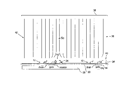
With reference to Figure 1, an active matrix 10 is
shown comprising a plurality of pixels, each comprising a
pixel electrode 12, storage capacitor 14 and thin film
transistor (TFT) 16. An external sc~n~i~g control
circuit 18 turns on the TFTs 16 one row at a time via a
plurality of control lines 19, for transferring the image
charge from the pixels to a plurality of data lines 20,
and then to respective external charge amplifiers 22. At
the same time, the input (virtual ground) of the charge
amplifiers 22 resets the potential at each pixel
electrode 12. The resulting amplified signal for each
row is multiplexed by a parallel-to-serial converter or
multiplexer 24, and then transmitted to an analog-to-
digital converter or digitizer 26.
- Each TFT 16 comprises 3 electrical connections: the
drain (D) is connected to the pixel electrode 12 and
pixel storage capacitor 14; the source (S) is connected
to a common data line 20 shared by all TFTs of the same
CA 022180~9 1997- lO- lO
WO 96/34416 PCT/CA95/00247
column, and also to an external charge sensitive
amplifier 22; and the gate (G) is used for control of the
"on" and "off" state of the TFT 16. Usually, lOV and -5V
is applied to turn on and off the TFT 16 respectively.
The scanning control circuit 18 may be fabricated as
a single crystal silicon integrated circuit which is wire
bonded to the active matrix TFT array. The charge
amplifiers 22 and multiplexer 24 may also be fabricated
as a single crystal silicon integrated circuit which is
wire bonded to the active matrix array.
Turning now to Figure 2, the structure of a single
pixel is shown of the large area integrated circuit
active matrix.
First, a metal layer (preferably Cr or Al) is
deposited (by thermal evaporation or sputtering) on a
glass substrate 28 and patterned using photolithography
to form the gate regions (G) for the array of TFTs. As
discussed in greater detail below, the gate line of an
ad~acent pixel may be ext~n~e~ so that the gate line and
the pixel electrode 12 form an integrated pixel storage
capacitor 14 with insulating layer 30 exten~i~g
therebetween. Alternatively, separate ground return
electrodes for storage capacitor may be formed between
gate electrode lines on the first metal layer. The
insulating layer 30 is deposited using PECVD (Plasma
~nhA~ce~ Chemical Vapour Deposition) or thermal
evaporation. The insulating material can be SiO2, Si3N4,
or alternate layers of both. The thickness of the layer
is typically 0.1 - 0.5 ~m.
Next, the drain (D) and source (S) metal layers are
deposited (by thermal evaporation or sputtering) and
patterned using photolithography to form drain and source
contact pads for the TFT, the pixel electrodes and source
(i.e. data) lines. The preferred material for the D and
S contact pads is Cr, and an extra coating of Al is
preferably added to the source lines to reduce the source
line resistance. Next, a semiconductor layer 32, being
CA 022180~9 1997-10-10
WO96/34416 PCT/CA95~00247
several hundred angstroms thick, is deposited (e.g. using
thermal evaporation or sputtering in the case of CdSe)
and then patterned using photolithography to form the TFT
~h~nn~l (e.g. 30 ~m wide and 50 ~m long, although the
illustrated TFT geometry represents only one possible
embodiment of the invention).
The above-described deposition procedure is used for
the drain, and source metal and semiconductor fabrication
steps for a bottom D and S contact TFT structure. The
two deposition steps can be reversed to form a top
contact structure.
Next a dielectric layer 34 (Sio2, Si3~ or alternate
layers of both) is deposited (using PECVD or thermal
evaporation) with a thickness of 0.3 - 5 ~m. Then, the
dielectric on top of the pixel electrode is etched away
to expose the pixel electrode.
The final top metal layer (preferably Al, or ITO) of
the TFT is deposited using sputtering or thermal
evaporation, and patterned using photolithography to form
the pixel ele~LLode 12 (which is the bottom pixel
electrode since the dielectric in this region has been
etched away). As ~;~r~csed in greater detail below,
according to the preferred embodiment, the pixel
electrode 12 extend~ over the top gate dielectric layer
34 so as to form a dual gate TFT structure. A blocking
layer may be formed by thermal oxidization the top metal
(Al) layer for preventing negative charge injection from
the pixel electrode to the X-ray photoconductor.
A uniform layer of X-ray sensitive photoconductor 36
is then directly deposited on the surface of the active
matrix by thermal evaporation, to a thickness of
approximately 500 ~m. Preferably, the photoconductor is
fabricated from amorphous selenium (a-Se).
A top bias electrode 38 is deposited (e.g. by
thermal evaporation) onto the photoconductor layer 36
with ay~L ~L iate blocking contact so that charge
generated in the bulk of the photoconductor can flow to
CA 022180~9 1997- lO- lO
WO 96/34416 PCTICA95/00247
the bias electrode, with no charge injection from the
bias electrode into the photoconductor. Several types of
metal may form the blocking contact with selenium, such
a8 Au, Indium, etc. An alternative embodiment is to
s deposit a thin layer (several hundred angstroms) of
insulator (e.g. CeO2) on the surface of the selenium
before the bias electrode is deposited, wherein the thin
insulating layer serves as a blocking layer.
Returning briefly to Figure lB, the selenium layer
36 and top bias electrode 38 are shown schematically as a
photodiode connected to a high bias voltage (HV) at the
cathode of each pixel.
During X-ray irradiation, the X-ray energy is
absorbed by the X-ray photoconductor 36 and electron-hole
pairs are created. Under the applied electric field
created by the difference in potential between bias
electrode 38 and pixel electrode 12, the radiation
generated charges are drawn to the surfaces of the
photoconductor 36 and collected on pixel electrode 12.
The difference in charge at each pixel represents the X-
ray image.
As ~ccllcsed above, the pixel electrode is connected
to the drain (D) of the TFT 16. During each readout, the
potential of the pixel electrode is reset, through the
TFT, to a ground potential by the virtual ground input of
the charge amplifier 22.
For fluoroscopy applications, a high voltage is
constantly applied to the bias electrode 38 and the
imaging detector is scanned in real time (i.e. 30 frames
per second). The images are acquired continuously in
every 1/30 second frame and are processed and displayed
in real time.
For radiography applications, a high voltage is
applied to the bias electrode 38 and the sc~n~i ng is
suspended (i.e. all TFTs 16 are turned off) during X-ray
Qxposure . Sc~nn ing is resumed immediately after the
Qxposure in order to readout the image.
CA 022180~9 1997-10-10
Wo 96134416 PCT/CA95100247
For a-Se, the photoconductor layer 36 needs to be of
a thickness in the order of 500 ~m in order to absorb
most of the incident X-rays. Thus, the bias voltage
applied to electrode 38 must be in the order of 5000
volts under an electric field of lOV/~m. Under abnormal
conditions (e.g. a false prolonged X-ray exposure when
all TFTs 16 are turned off), the potential on each pixel
(Vp) can reach a damaging high value (e.g. 1000 volts).
The CdSe TFTs 16 of the preferred embodiment can maintain
normal functions at Vp up to approximately 200 volts.
Thus, it is necessary to ensure that even under false,
abnormal conditions, Vp does not exceed 100 volts.
As discl~ce~ briefly above, and as shown with
reference to Figure 2, a dual gate structure is utilized
to protect the TFT 16 from high voltage damage. In
particular, the pixel electrode 12 (which is connected to
the TFT drain (D)), extends over the top of the TFT 16
and acts as a second gate. The top gate voltage is
equivalent to the pixel voltage (i.e. VTa=Vp).
By adjusting the thickness of the top dielectric
layer 34, the effect of Vp on the transfer characteristics
of the TFT 16, can be controlled. The top dielectric
layer 34 is usually 5 to 10 times the thickness of the
bottom gate dielectric layer for high voltage protection
at a pixel potential of 100 volts. Figure 3 shows the
ID_V~ characteristic curve for a dual gate TFT at
different values of Vp. Under normal imaging conditions
(i.e. Vp<10 V), the bottom gate control pulse causes the
TFT 16 to turn on and off correctly. However, if Vp
eYc~eAR 100 volts, the bottom gate control pulse is no
longer able to turn off TFT 16. In this case, the high
leakage current drains away the excess charge on the
pixel electrode 12 and Vp never reaches a dangerously high
- potential.
The relationship between maximum pixel voltage V
and dielectric thickness may be expressed as follows:
CA 022180~9 1997-10-10
WO 96/34416 PCT/CA95/00247
~i, = g~ x
d~ V~ d~
where ~ is the dielectric constant of dielectric layer
34, d~ is the thickness of dielectric layer 34, V~ is
the maximum voltage to be applied to the pixel, ~
dielectric con6tant of the dielectric layer 30, and d~ is
the thickness thereof. When Va(~ (usually -5V) is applied
to the bottom gate (G), it is desired that the TFT will
nonetheless turn on when the voltage applied to pixel
electrode 12 reaches Vp(m~). V~ is a constant representing
the minimum voltage which when applied to the bottom gate
(G) will turn on the TFT when VpzO. Thus for a dielectric
layer 30 having thickness in the range of 0.1 to 0.5 ~m,
a maximum pixel voltage of 100 volts, and the constant V~
of 10 volt~, the dielectric layer 34 will have a
thickness of 1-5 ~m, given the same dielectric as the
dielectric layer 30.
Another co~C~quence of making the photoconductor
layer 36 thick to absorb as much X-ray energy as
possible, i~ that a small sensor capacitance is created
for each pixel (e.g. approximately 0.01 pF). This can
result in three problems. Firstly, the pixel voltage Vp
on the drain (D) of the TFT 16 rises rapidly with the
image charge (e.g. approximately 100 V/pC) because of the
small pixel capacitance (i.e. the sum of the sensor
capacitance C& and the coupling capacitance between the
gate and drain of the TFT (CaD)), which in turn can cause
high voltage damage to the TFTs 16 and the external
electronics (e.g. ccAnn~ng control circuit 18, charge
amplifiers 22, multiplexer 24). Secondly, when each TFT
16 i8 turned off, charge injection to the pixel electrode
12 by the negative edge of the gate pulse output from
rCAnning control circuit 18 (e.g. 15 volts), results in a
negative potential on the pixel and thus a small forward
bias between the gate (G) and drain (D). This can cause
a significant increase in the leakage current for the TFT
16. Thirdly, the charge leakage time constant for each
CA 022180~9 1997-10-10
PCT/CA95/00247
Wo 96/34~16
13
pixel Cp x ~ff (approximately 10l3 n) is lOOmS. For
radiography applications, the pixels that are read out
last will thus experience significant signal loss due to
the short leakage time constant.
According to the preferred embodiment, an integrated
pixel storage capacitance (C~) is provided on the TFT
active matrix array, by overlapping the pixel electrode
12 with the gate line (G) of an adjacent pixel, as shown
in Figure 1 and in Figure 2 on the left where storage
capacitor 14 is formed by overlapping pixel electrode 12
with an extension of the gate line (G) of an adjacent
pixel. As an alternative to overlapping the pixel
electrode 12 with the adjacent gate line, a separate
ground line may be utilized. A large pixel capacitance
results from the thin insulating layer 30 (typically 0.1
- 0.5 ~m), resulting in a storage capacitance C~ in the
range of 0.5 - 1 pF, which is 20 times larger than CaD,
and two orders of magnitude larger than the capacitance
of the photoconductor layer 36. The value of C~ is
achieved by ext~;ng the pattern of the gate electrode
(or a separate ground line), under the region of each
pixel electrode 12 when the size of the pixel electrode
is larger than 200 ~m (e.g. for fluoroscopy and general
radiography). For mammography applications, since the
pixel size must be smaller tin the order of 50 ~m),
thinn;ng of the insulator is needed in addition to
exte~in~ the gate electrode.
The large integrated pixel storage capacitance C~
ensures, firstly, that the pixel voltage Vp does not rise
more than 2V/pC with image charge, and thus does not
reach a damagingly high potential under diagnostic X-ray
exposure levels. Secondly, the voltage on the pixel
electrodes returns to near ground potential after the
TFTs 16 are turned off, thereby ensuring a low leakage
current. Thirdly, the charge leakage time constant is
approximately 10 seconds, and thus does not cause any
significant signal loss for radiography applications.
CA 022180~9 1997-10-10
WO 96/34116 PCT/CA95/00247
14
Turning to Figure 4, a cross sectional view, is
provided similar to Figure 2, through two adjacent
pixels. However, the section of Figure 2 extends through
storage capacitor 14, while the section of Figure 4 does
not. According to the embodiment illustrated in Figure
4, a plurality of parallel rails 40 are deposited as a
grid adjacent the pixel electrodes 12, so as to overlay
the source lines (S). Image charge collection efficiency
in an active matrix sensor array, is controlled by the
fill factor (i.e. the fraction of the area of each pixel
that is occupied by the pixel electrode 12). The fill
factor of a typical CdSe TFT array is approximately 80%
for a 200 ~m square pixel. Most of the remainder of each
pixel is occupied by the source lines (S). By applying a
potential on the grid 40 that is significantly higher
than the pixel potential, the electric field distribution
in the photoconductive layer 36 may be manipulated so
that image charges only land on the pixel electrodes 12,
and not on the source lines (S). As seen in Figure 4,
the field lines 42 may be caused to bend toward the pixel
electrodes 12 and thus increase the effective fill
factor. In practice, the potential applied to the grid
40 must be sufficient to cause a noticeable increase in
charge collection efficiency of the pixel electrode 12
(e.g. typically in the order of several hundred volts).
A plan view of the grid 40 is shown in Figure 4B.
With reference to Figure 4C, instead of utilizing a
grid to bend the field, as in the embodiment of Figures
4A and 4B, the charge trapping properties of the top
dielectric material of the pixel electrodes may be
utilized to bend the electric field. More particularly,
after the construction of the detector is completed, a
seasoning process is performed. To perform this
seasoning, the detector is exposed to large doses of X-
rays (or visible light if the top bias electrode 38 issemitransparent, e.g. Au), with the TFTs 16 all turned on
and with an electric field applied to the selenium
CA 022l80~9 l997- lO- lO
WO 961344l6 PCT/CA95/00247
photoconductor 36. The holes created in the
photoconductor 36 are drawn to the bottom surface
thereof, either landing on the pixel electrodes 12 or
becoming trapped by the dielectric material 34 between
pixel electrodes. Holes which land on the pixel
electrodes 12 are drained away through the turned-on TFTs
16 and the holes trapped at the insulator 34 generate a
surface potential which increases with the number of
holes trapped. When the potential rises to a level
wherein further holes are repelled from the insulator,
the system has reached equilibrium. Since the trapping
of holes is a long term effect, when the detector is used
for imaging after this stage, X-ray created holes will
prefer to land on the pixel electrodes 12 and the
effective fill-factor of the system is thereby increased
to nearly 100%. This seasoning process may be performed
once after the detector is constructed, or may be
performed at the beg; nn; ~g of each day during which
imaging is expected to be performed. It is further
contemplated that repeated seasoning may not be necessary
after long term usage of the device since the dark
current of selenium may be enough to perform hole
repelling after a sufficient term of use.
According to a further aspect of the present
invention, means for measuring X-ray exposure dosages may
be incorporated into the design of the active matrix flat
panel detector so as to perform photo timing functions
simultaneously with image detection.
Figure 5 shows the top view of top sensor bias
electrode 38 which, as discussed above, is connected to a
high voltage power supply. A plurality of smaller
electrodes 42 (e.g. preferably 3 for chest radiography)
provide regions of X-ray dose measurement.
- The bias electrode 38 is connected to a DC high
voltage (HV) power supply. Each phototimer electrode 42
is connected to its own dose/dose rate measurement
circuit. As shown in Figure 7, each electrode 42 is
CA 022180~9 1997-10-10
WO 96/34416 PCTICA95/00247
connected to the inverting input of an amplifier 71 which
i8 powered by a pair of isolated power supplies, for
providing +15V and -15V with the ground reference set at
the DC HV bias potential applied to the photoconductor
36. The inverting input of amplifier 71 is at the same
potential as its non-inverting input, which is connected
to the DC HV bias. Therefore, electrode 42 is at the
same potential as electrode 38. When X-rays are absorbed
by the photoconductor 36, current generated in the region
of the phototimer flows to the amplifier 71 (since a
closed loop circuit is provided by the storage capacitors
14 and C~D) . In the case of fluoroscopy, the X-ray
generated current is measured with a feed-back resistor
73 at the amplifier, resulting in an output voltage
signal which is, in turn, measured by a circuit in the X-
ray generator (not shown) to determine whether it is the
expected value and therefore whether to change the X-ray
tube current. In the case or radiography, the
photocurrent generated during a short pulse (a fraction
of a second) of X-ray exposure is integrated by the feed-
back capacitor 75 of the amplifier. When the amplifier
71 ouL~L voltage (also monitored by a circuit in the X-
ray generator) reaches a preset value (i.e. proportional
to the preset X-ray exposure dosage), the X-ray generator
will turn off the X-rays.
The imaging mode (fluoroscopy or radiography) is
selected electronically by a relay 77. Since the relay
77 is connected to the amplifier circuit, it has to be
operated by a control signal with the same reference
(i.e. DC HV potential).
In the cross sectional view of the Figure 6A
emho~iment, a gap 43 is provided for isolating the
phototimer bias electrodes 42 from the common top bias
electrode 38, whereas in the cross-sectional view of the
Figure 6B embodiment no gap for electric field
application is shown (when viewed in plan), and the
n~C~C~ry isolation between electrodes is provided by an
-
CA 02218059 1997-10-10
WO 96/34416 PCT/CA95~00247
17
additional insulation layer 44.
Other embodiments and variations of the invention
are possible. All such modifications and variations are
believed to be within the sphere and scope of the
invention as defined by the claims appended hereto.