Note: Descriptions are shown in the official language in which they were submitted.
CA 02218262 1997-10-15
C A N A D A
APPLICANT: NIPPON TELEGRAPH AND TELEPHONE CORPORATION
TITLE: ULTRA-HIGH-SPEED SEMICONDUCTOR OPTICAL
MODULATOR WITH TRAVELING-WAVE ELECTRODE
CA 02218262 2000-02-O1
This invention relates to a semiconductor optical
modulator, more specifically to an ultra-high speed
semiconductor optical modulator with a traveling-wave
electrode which operates at a low driving voltage, with
reduced loss and in ultra-wide bandwidth.
The present invention can be applied to a future
ultra-high capacity optical transmission system to be used
in the U.S. and Europe.
High-speed semiconductor optical modulators studied
for future high-density transmission systems can be
categorized into two types. One is an electro-absorption
(E-A) optical modulator with a lumped-element (L-E)
electrode. The other is an electro-optic (E-O) optical
modulator with a traveling-wave (T-W) electrode. The
following will discuss a semiconductor electro-absorption
optical modulator with a lumped-element electrode and a
semiconductor electro-optic optical modulator with a
traveling-wave electrode.
Figure 1 shows a bird-view of a conventional
semiconductor electro-absorption optical modulator with a
lumped-element electrode. In this Fig. 1 is the p-
electrode, 2 is the p+-InGaAs cap layer, 3 is the p-InP
- 1 -
CA 02218262 1997-10-15
cladding layer, and 5 is the core. Here, an i-InGaAlAs(13
nm)/InAlAs(5 nm) multi-quantum well (MQW) core is assumed
to be used for a core. Six is a n-InP cladding, 7 is a n-
InP substrate, 8 is a n-electrode, and 9 is a polyimide.
Here, the electrode on the polyimide 9 is called a bonding
pad and 10 is a bonding wire. The electric signal
supplied by a signal generator is applied to the bonding
wire 10.
In order to explain the operation principle of a
semiconductor electro-absorption optical modulator, an
optical absorption spectrum of the MQW core 5 is shown in
Fig. 2. The optical absorption peak is set at around 1.49
~m for a signal light of 1.55 ~tm. As shown in this
figure, since the difference between the wavelength of the
operating signal light and the wavelength of the
absorption edge is large for the zero-biased condition
(solid line A), the incident wave can be emitted without
suffering significant absorption. Thus, the ON-state can
be achieved. On the other hand, since the absorption
spectrum is shifted toward the long wavelength region
under the reverse-biased condition (broken line B), the
signal light is absorbed in the i-MQW core, 5. This
results in the OFF-state.
The p-electrode, 1, of this conventional
semiconductor optical modulator is used for lumped-element
operation. In order to explain the operation, Fig. 3
shows an equivalent circuit, which includes a driving
signal generator. Here, SG is a driving signal generator,
- 2 -
CA 02218262 1997-10-15
RG is its characteristic impedance, RL is a termination
resistor, CMQW is the capacitance of the i-MQW core, 5, and
CP is the capacitance of the above-mentioned bonding pad.
The electrical 3-dB bandwidth, ~fel, for this structure
can be approximately expressed as,
~fel - 1/ (?L~RL'CMQw) .
Generally, the termination resistor RL has the same
characteristic impedance of 50 S2 as that (RG) of the
driving signal generator SG. Here, we assumed that since
the capacitance of the pad is sufficiently small, the
total capacitance can be determined by the capacitance of
the i-MQW core, 5. Tr~hen we assume that the thickness (d),
width (W) and length (L) of the i-MQW core, 5, are
respectively 0.2 Vim, 2 ~m and 300 Nxn, the capacitance of
the i-MQW core, 5, can be obtained from the following
equation,
CMQW = ~o'~r'W'L/d. (2)
Here, Eo and Er are respectively the dielectric
constant of the vacuum and the relative dielectric
constant of the i-MQW core, 5.
From the Eqs. (1) and (2), the electrical 3-dB
bandwidth, Ofel, for the above-mentioned semiconductor
lumped-element optical MQW modulator is around 20 GHz or
less. Although the electrical 3-dB bandwidth, Ofel, can
be improved by using smaller value of CMQW, the extinction
ratio of the signal light is degraded. When we assume that
D is the increase of the absorption coefficient and h is
the confinement factor of the propagating field into the
- 3 -
CA 02218262 1997-10-15
i-MQW core, 5, the extinction ratio, R, of the signal
light can be expressed as,
R = exp(-006~r~L) . (3)
As shown in this equation, a too short i-MQW core, 5,
degrades the extinction ratio. Thus, a too short i-MQW
core, 5, cannot be used from the view-point of the
extinction ratio.
As explained above, there is a severe trade-off
between the electrical 3-dB bandwidth Ofef, which is
limited by the CR-constant, and the extinction ratio.
Thus, there is a great difficulty for realizing an ultra
high-speed semiconductor optical modulator with a 50 GHz
modulation bandwidth and a high extinction ratio.
The conventional semiconductor optical modulator with
a traveling-wave electrode makes use of the electro-optic
effect which means that the refractive index is changed by
applying the biased voltage (R. SPICKERMANN et al., IEE
Electronics Letters, vol. 32, pp. 1095-1096, 1996). The
semiconductor optical modulator's equivalent circuit is
shown in Fig. 4. As is well known, the modulation index,
m(f), can be expressed as (S. H. Lin et al., Applied
optics, vol. 26, pp. 1696-1700, 1987),
m f ~1 rl r2 J exp~ j/3o L ~ V + r V
1+r x ~ + 2
2 ~~2 p~~L3e L) - rl r2 exp~-~/~e L~)
- 4 -
CA 02218262 1997-10-15
V ~ = eXp (+~~~ ) sin ø~ / ~~
~~ _ ~~e - ~o ~L / 2
I30 = C~ml~O lCO
~e = l,~ml2m lCO _ Jlrm
T, _ Z -RG (5)
Z + RG
__ Z - RL
Z + RL ,
where L is an interaction length between the electric
signal and light, i. e. the length of the traveling-wave
electrode. And, no and nm are respectively the effective
indexes of the optical wave and electric signal. Here,
(~ is the angular frequency of the electric signal, Cp is
light velocity in the vacuum, oGm is the microwave
attenuation factor, and Z is the characteristic impedance
of the semiconductor optical modulator using the
traveling-wave electrode.
Since the characteristic impedance of the
conventional optical modulator is 50 S2, the non-doped
layer, which does not have intentional doping, is thick.
Furthermore, the electro-optic effect, i.e. index change
effect, is small even for the case of a MQW core
- 5 -
CA 02218262 1997-10-15
structure. Thus, the traveling-wave electrodes have long
interaction lengths of the order of millimeters.
Next, the influence of the electrode length on the
modulation bandwidth will be qualitatively discussed. For
simplicity, by assuming the velocity matching between
electric signal and light (nm = no) and impedance matching
between a semiconductor optical modulator and outer
circuits (Z - RG = RL), the following simple relation can
be obtained from Eq. (4) for the modulation bandwidth, 0f,
0f ~ 1/ (OC~,L)2. (6)
Therefore, long traveling-wave electrodes
significantly degrade the modulation bandwidth due to the
electrode conductor loss.
Thus, it was almost impossible to realize a high-
speed semiconductor electro-optic optical modulator with a
low-driving voltage by making use of a traveling-wave
electrode.
Recently, one traveling-wave semiconductor electro-
absorption modulator has been reported (N. Agrawal, et
al., European conf. Integ. Opt. (ECIO), 1997, Paper EFB3-
1). It has a relatively short interaction length (500
N.m), but its modulation bandwidth was limited to 18 GHz
(3-dB electrical) and no data has been reported on the
driving voltage, intrinsic layer thickness, and
characteristic impedance.
The present invention provides an ultra-high speed
semiconductor optical modulator with a traveling-wave
- 6 -
CA 02218262 1997-10-15
electrode which is superior in optical modulation
bandwidth.
The present invention further provides a
semiconductor optical modulator, which has both advantages
of a lumped-element electrode construction and a
traveling-wave electrode construction, is low in driving
voltage and insertion loss, and has optical modulation
characteristics of ultra-wide bandwidth.
A first aspect of the present invention, an ultra-
high speed semiconductor optical modulator with a
traveling-wave electrode comprising a semiconductor core
which is shorter in absorption-peak wavelength than a
wavelength of optical signal, and an electrode for
applying an electric signal to absorb the optical signal
by shifting the absorption-peak wavelength to a long
wavelength region when the voltage is applied, wherein the
electrode is constructed in the form of a traveling-wave
electrode, which can be applied with an electric signal to
one end thereof and an electric signal can be taken out
from the other end.
Here, the other end of the traveling-wave electrode
may be connected with a termination resistor.
Further, a characteristic impedance of an outer
circuit connected to the other end may be equal to the
characteristic impedance of the optical modulator.
Still further, a non-doped semiconductor layer may be
provided between the semiconductor core and an upper
cladding layer located thereabove. A non-doped
CA 02218262 1997-10-15
semiconductor layer may be provided between the
semiconductor core and a lower cladding layer located
therebeneath. Yet further, non-doped semiconductor layers
may be provided individually between the semiconductor
core and the upper cladding layer located thereabove, and
between the semiconductor core and the lower cladding
layer located therebeneath.
In the first aspect of the present invention, a
voltage is applied and thereby the absorption-peak
wavelength of the semiconductor core is shifted to the
long wavelength region, whereby forming the electrode for
applying the voltage to absorb the optical signal into the
semiconductor core as a traveling-wave electrode. More
specifically, an electric signal (i.e. voltage) input port
is provided at the optical signal input side, and an
electric signal output port is provided at the optical
signal output side. With this construction, the electric
signal and optical signal run in the same direction. With
the construction according to the present invention, a
problem in that an electrical 3-dB bandwidth Ofel is
limited by CR constant is eliminated. Therefore, in
particular, when the electric signal and optical signal
are velocity matched, length of the semiconductor core for
absorbing light when light is off can be increased,
thereby achieving ultra-high speed optical modulation
while maintaining a high extinction ratio.
A second aspect of the present invention, an ultra-
high speed semiconductor optical modulator with a
_ g _
CA 02218262 1997-10-15
traveling-wave electrode comprising a semiconductor core
shorter in absorption-peak wavelength than a wavelength of
optical signal, and an electrode for applying an electric
signal to absorb the optical signal by shifting the
absorption-peak wavelength to a long wavelength region
when the voltage is applied, wherein the electrode is
constructed in the form of a traveling-wave electrode,
which can be applied with an electric signal to one end
thereof and an electric signal can be taken out from the
other end, and a total thickness of non-doped
semiconductor layers including the semiconductor core is
decreased so that a driving voltage of electric signal is
reduced.
Here, by decreasing the interaction length of the
electric signal and optical signal, degradation of optical
modulation bandwidth and reflection characteristics of
electric signal due to a characteristic impedance
mismatching between an outer circuit and the traveling-
wave electrode caused by decreasing the total thickness of
non-doped semiconductor layers including the semiconductor
core may be reduced.
Further, by adjusting a doping concentration of a p-
type doped layer located above or beneath the
semiconductor core, the mismatching of the characteristic
impedance may be corrected. Still further, by adjusting
the doping concentration of an n-type doped layer located
above or beneath the semiconductor core, the mismatching
of the characteristic impedance may be corrected.
- 9 -
CA 02218262 1997-10-15
Yet further, the non-doped semiconductor layer may be
free of a semiconductor layer other than the semiconductor
core. Yet further, in the non-doped semiconductor layer,
the semiconductor layer other than the semiconductor core,
if present, may be very small in thickness.
Yet further, the total thickness of the non-doped
semiconductor layers including the semiconductor core may
be less than approximately 0.5 ~..Lm. Yet further, the
interaction length of the electric signal and optical
signal may be less than approximately 400 (,gym. Yet
further, the characteristic impedance of the traveling-
wave electrode may be less than approximately 40 S2.
Yet further, it may be that the total thickness of
non-doped semiconductor layers including the semiconductor
core is less than approximately 0.5 ~,m, the interaction
length of the electric signal and optical signal is less
than approximately 400 ~.m, and the characteristic
impedance of the traveling-wave electrode is less than
approximately 40 SZ.
Yet further, the other end of the traveling-wave
electrode may be connected with a termination resistor.
With the second aspect of the present invention,
since the total thickness of non-doped semiconductor
layers is decreased, an electric field strength in a MQW
core increases and, as a result, a shift amount in
absorption-peak wavelength of the MQW core can be
increased, thereby reducing the driving voltage necessary
for obtaining a desired extinction ratio.
- 10 -
CA 02218262 1997-10-15
Yet further, when the total thickness of non-doped
semiconductor layers is decreased, there may be a case in
which the characteristic impedance is decreased and, as a
result, degradations in optical modulation bandwidth and
reflection of the electrical signal are caused. However,
this decrement of the characteristic impedance can be
compensated by setting an interaction length L of electric
signal and light to a shorter value, and optical insertion
loss can be suppressed thereby.
Yet further, by adjusting the doping concentration of
the doped layer located above or beneath the MQW core,
mismatching of the characteristic impedance can be
compensated, thereby optical modulation of wider bandwidth
can be achieved and the reflection of the electrical
signal can be suppressed.
Therefore, according to the present invention, a
semiconductor optical modulator can be achieved which has
both advantages of lumped-element electrode construction
and traveling-wave electrode construction, is low in
driving voltage, and has ultra-wide-band optical
modulation characteristics.
The above and other objects, effects, features and
advantages of the present invention will become more
apparent from the following description of the embodiments
thereof taken in conjunction with the accompanying
drawings.
- 11 -
CA 02218262 1997-10-15
Figure 1 is a schematic view showing the structure of
a prior art semiconductor electro-absorption optical
modulator with a lumped-element electrode;
Figure 2 is a graph showing an optical absorption
spectrum characteristic of MQW core of the prior art
semiconductor optical modulator;
Figure 3 is a circuit diagram showing an equivalent
circuit including an outer driving circuit and a prior art
semiconductor optical modulator with a lumped-element
electrode;
Figure 4 is an equivalent circuit diagram when
operating a prior art semiconductor optical modulator with
a traveling-wave electrode utilizing a change in
refractive index;
Figure 5 is a schematic view showing the structure of
the semiconductor optical modulator with a traveling-wave
electrode according to a first embodiment of the present
invention;
Figure 6 is a graph showing the relationship between
total thickness of non-doped layers D of MQW core shown in
Fig. 5 and a driving voltage;
Figure 7 is a schematic view showing the structure of
the semiconductor optical modulator with a traveling-wave
electrode according to a second embodiment of the present
invention;
Figure 8 is a graph for explaining the principle of
the second embodiment according to the present invention,
showing an influence of microwave propagation loss Oc,~ of a
- 12 -
CA 02218262 1997-10-15
traveling-wave electrode on optical modulation
characteristics when the microwave propagation loss oG is
smal 1 ( ocn, = 5 dB / cm ) ;
Figure 9 is a graph for explaining the principle of
the second embodiment according to the present invention,
showing an influence of microwave propagation loss ocm of a
traveling-wave electrode on optical modulation
characteristics when the microwave propagation loss 0~, is
large (ocm = 20 dB/cm) ;
Figure 10 is a graph for explaining the principle of
the second embodiment according to the present invention,
showing calculation results of optical modulation
characteristics when the microwave propagation loss oc~, of
the traveling-wave electrode is very large (ocj" = 100
dB/cm);
Figure 11 is a graph for explaining extinction
characteristics vs. applied voltage of the semiconductor
MQW modulator of the first embodiment shown in Fig. 5;
Figure 12 is a graph for explaining a dependence of
the length of i-MQW core on driving voltage of the
semiconductor MQW modulator of the first embodiment shown
in Fig. 5;
Figure 13 is a graph for explaining the principle of
the second embodiment according to the present invention,
showing optical modulation characteristics when a
characteristic impedance z is apparently 3552;
Figure 14 is a graph showing optical modulation
characteristics of an optical modulator fabricated by
- 13 -
CA 02218262 1997-10-15
applying the second embodiment according to the present
invention;
Figure 15 is a graph showing extinction
characteristics of an optical modulator fabricated by
applying the second embodiment according to the present
invention;
Figure 16 is a schematic top view showing the
structure of the semiconductor optical modulator with a
traveling-wave electrode according to the third
embodiment;
Figure 17 is a schematic cross-sectional view of the
third embodiment of the semiconductor optical modulator
with a traveling-wave electrode shown in Fig. 16 at XVII -
XVII;
Figure 18 is a schematic cross-sectional view of the
third embodiment of the semiconductor optical modulator
with a traveling-wave electrode shown in Fig. 16 at XVIII
- XVIII.
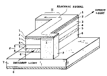
<First embodiment>
A first embodiment of the present invention is shown
in Fig. 5. In the figure, as in the prior art example,
the reference numeral 1 indicates a p-side electrode, 2 is
a p+-InGaAs cap layer, 3 is a p-InP cladding layer, 5 is a
core layer, and also in the present embodiment, an i-
InGaAlAs (130 ~)/InAlAs(50 ~) multi-quantum well (MQW) is
exemplified. The reference numeral 6 indicates an n-InP
cladding layer, 7 is an n-InP substrate, and 8 is an n-
- 14 -
CA 02218262 1997-10-15
side electrode. The reference numeral 9 indicates a
polyimide layer, and 4 is an i-InP layer. Such a
structure can be fabricated by a conventional
semiconductor device fabrication technology.
Here, a major difference of the present embodiment
from the prior art example shown in Fig. 1 is that the A-
side electrode, 1, is a traveling-wave electrode. The
electrode located above the polyimide layer, 9, is an
electric signal input port, I, which is inputted with an
electric signal (reverse-bias voltage) from a driving
signal generator (not shown). On the other hand, an
output port, II, is provided on the electrode of the
optical signal output side, which is connected with a
termination resistor. That is, during the time when light
is inputted and propagates in the i-MQW optical modulator,
the electric signal also propagates in the same direction
over the entire length of the optical modulator. Since,
during the time when both signals run in the same
direction, by the electric signal the absorption-peak
wavelength of the i-MQW core is shifted to the long
wavelength region, as a result, the light is absorbed
resulting in the off-state.
In the present embodiment, the p-side electrode, 1,
is a traveling-wave electrode. However, since the
characteristic impedance of the electric signal generator
SG is 50 SZ, it is desirable that the characteristic
impedance of the electro-absorption MQW is equal to or in
the vicinity of 50 SZ. Therefore, in the present
- 15 -
CA 02218262 1997-10-15
embodiment, the i-InP layer, 4, is provided between the
MQW core, 5, and the p-InP cladding layer, 3, so that the
characteristic impedance of the MQW modulator including
the p-side electrode, 1, is 50 S2. The termination
resistor connected to the output port, II, of the
electrode 1 has a resistance of 50 S2.
The electrical 3-dB modulation bandwidth Ofel of the
semiconductor electro-absorption optical modulator with
the traveling-wave electrode, for simplicity, when the
microwave propagation loss of the traveling-wave electrode
is assumed as 0 and the characteristic impedance as 50 S2,
is represented as
~fel= 1. 4 Co/ (~~~ nm - no ~ ) L) .
Here, co is light velocity, nm is an effective index of
the MQW optical modulator to the electric signal, no is an
effective index of the modulator to the signal light, and
L is an interaction length of the traveling-wave electrode
and the i-MQW core 5. Therefore, from Eq. (7), when L is
set at 300 ~.m, nm at 3.4, and no at 3.2, ultra-wide-band
optical modulation can be achieved with Ofel of about 2200
GHz.
Further, when the electric signal and optical signal
are velocity matched, that is, when nm = no, the bandwidth
limitation factor is only the microwave propagation loss
of the electrode even when the length L of the i-MQW core,
5, is increased to increase the extinction ratio R of
- 16 -
CA 02218262 1997-10-15
light. Since the microwave propagation loss can be
reduced by increasing the thickness of the electrode and
so on, this can also achieve ultra-wide-band operation of
the optical modulator.
Still further, in the present embodiment, the entire
multilayer structure above the lower cladding layer, 6, is
ridge-formed and the side surface of the i-MQW core is
exposed to the air. That is, a so-called high-mesa-
structured optical modulator is shown. Of the multilayer
structure, only part of the i-InP layer 4, the upper
cladding layer, 3, the InGaAs cap layer, 2, and the p-side
electrode, 1, may be ridge-formed to form a so-called
strip loaded configuration.
Yet further, in the present embodiment, the i-InP
layer, 4, is provided between the i-MQW core, 5, and the
upper cladding layer, 3. However, the i-InP layer may be
provided between the i-MQW core, 5, and the lower cladding
layer, 6. This construction avoids increasing of signal
voltage to produce a depletion layer in the i-MQW core, 5,
particularly even when the purity of the non-doped MQW
core and the InP layer is not sufficiently high. Of
course, the non-doped InP layer may be provided both above
and beneath the MQW core, 5.
Since, in the present invention, it is sufficient
that the electrode is a traveling-wave electrode, needless
to say configurations of the p-side and n-side electrodes
are not important, and a semi-insulating substrate may be
used as the substrate. Further, the i-MQW core, 5, may be
- 17 -
CA 02218262 1997-10-15
other MQW compositions such as i-InGaAs/InP, and it is
also possible to use a quarternary bulk composition such
as i-InGaAsP.
As described above, with the first embodiment of the
present invention which uses a traveling-wave electrode, a
semiconductor electro-absorption optical modulator which
is superior in terms of optical modulation bandwidth can
be achieved without degrading the extinction ratio.
<Second embodiment>
In the first embodiment of the present invention, the
p-side electrode, 1, for applying the electric signal is a
traveling-wave electrode, that is, during the time when
light is inputted and propagates in the MQW optical
modulator, the electric signal also propagates in the same
direction as the light over the entire length of the
optical modulator and the modulation characteristics is
determined from Eq. (4). Since, during the time when both
signals run in the same direction, by the electric signal
the absorption-peak wavelength of the i-MQW core, 5, is
shifted to the long wavelength region, then the light is
absorbed resulting in the off-state. Further, since the
electrode is a traveling-wave electrode, the p-side
electrode, 1, as shown in Fig. 5, is provided with an
electric signal input port, I, and output port, II. The
output port is connected with a 50 S2 termination
resistor.
- 18 -
CA 02218262 2000-02-O1
Since, in general, the characteristic impedance of
the electric signal generator SG is 50 SZ, in the first
'embodiment, it is considered that the characteristic
impedance of the traveling-wave electrode is preferably
equal to or in the vicinity of 50 S2, the thickness D of
the non- doped layers is increased by providing the i-InP
layer, 4, between the MQW core, 5, and the p-InP cladding
layer, 3, so that the characteristic impedance of the MQW
modulator including the p-side electrode, 1, is 50 52,.
As well known, shift amount of absorption-peak
wavelength of the i-MQW core, 5, is proportional to the
square of electric field strength applied. Specifically,
when the thickness of the i-InP layer 4 is increased so as
to set the characteristic impedance Z of the traveling-
wave electrode at 50 S2, the electric field in the i-MQW
core, 5, is decreased inversely proportional to the total
thickness D of the non-doped layers, however, the shift
amount of absorption-peak wavelength of the i-MQW core, 5,
is decreased inversely proportional to the square of the
total thickness D as described above. Therefore, the
driving voltage to obtain a desired extinction ratio is
increased proportional to the square of the total
thickness D of the non-doped layers.
Figure 6 shows this condition when the thickness of
the MQW core, 5, is 0.2 ~..~.m (driving voltage to achieve an
extinction ratio 20 dB is 1.5 V). That is, when the
thickness of the i-InP layer, 4, is increased so that the
characteristic impedance Z of the traveling-wave electrode
- 19 -
CA 02218262 1997-10-15
is in the vicinity of 50 S2, the driving voltage is
increased. It can be recognized from Fig. 6 that, for
example, when the total thickness of the non-doped layers
is assumed as 0.6 ~.m, the driving voltage is as high as
13.5V.
The i-MQW core, 5, has a length of 200 ~.~.m. The value
of 0.6 ~.tm of the non-doped layers described here is the
maximum thickness in the experiments ever conducted. In
order to achieve an actual 50 S2 system, it is necessary
that the total thickness D of the non-doped layers is
about half the width of the ridge, that is, about half the
width of the i-MQW core, 5, in Fig. 11. Therefore, when
the ridge width is assumed as about 2 ~,m which is a width
of common optical waveguides, the total thickness D of the
non-doped layers is as large as about 1 ~m and then the
driving voltage is considerably increased.
On the other hand, where an increase in absorption
coefficient of the i-MQW core, 5, by applying voltage is
a confinement factor (confinement rate) of the guided
wave to the i-MQW core, 5, is h, and an interaction length
of the traveling-wave electrode and the optical waveguide
comprising the i-MQW core, 5, is L, an extinction ratio R
of the electro-absorption optical modulator is represented
by Eq. (3) shown above (K. Kawano et al., IEEE Journal of
Quantum Electronics, vol. 28, pp. 224-230, 1992).
Then, as can be seen from Eq. (3) shown above,
degradation of electric field in the i-MQW core 5 by
increasing the total thickness D of the above-described
- 20 -
CA 02218262 1997-10-15
non-doped layers and, in turn, degradation in extinction
ratio can be compensated by increasing the interaction
length L of electric signal and light. As described
above, in the arrangement of the first embodiment shown in
Fig. 5, it is necessary to increase the interaction length
L. However, in the electro-absorption optical modulator,
since the absorption-peak wavelength of the i-MQW core, 5,
is relatively close to the operating wavelength (for
example, for an operating wavelength of 1.55 ~xn,
absorption-peak wavelength is 1.49 ~tm), as can be seen
from the light absorption factor shown by the following
formula,
exp(-OGO~ I~' ~L) , (8)
propagation loss of light is increased when voltage is not
applied and, as a result, insertion loss as the optical
modulator is increased. Here, oc0 is a light absorption
coefficient at the operating wavelength when a voltage is
not applied.
That is, the semiconductor electro-absorption optical
modulator with the traveling-wave electrode according to
the first embodiment still has a point that has yet to be
solved in that the driving voltage is increased or
insertion loss is high.
Then, the second embodiment of the present invention
provides a semiconductor electro-absorption optical
modulator with a traveling-wave electrode, which is
- 21 -
CA 02218262 1997-10-15
superior in terms of the driving voltage and insertion
loss.
Figure 7 shows the structure of the wide-band
semiconductor electro-absorption optical modulator
according to the second embodiment of the present
invention. Here, same as the first embodiment shown in
Fig. 5, the i-MQW core, 5, comprises, for example, an
InGaAlAs well (thickness: 130 ~) and an InAlAs barrier
(thickness: 50 ~), the total thickness thereof is about
0.1 to 0.5 Nm. The i-MQw core, 5, has a width of about 1
to 2 Vim. Unlike the first embodiment shown in Fig. 5, the
second embodiment of the present invention has not the i-
InP layer, 4, or if present, since it is very thin, as can
be seen from Fig. 6, there is no increasing factor of the
driving voltage. Therefore, it can be seen that the
semiconductor electro-absorption optical modulator
according to the second embodiment of the present
invention operates at a low driving voltage. However, the
characteristic impedance Z of the traveling-wave electrode
is lower than 50 SZ (for example, about 20 SZ) . If the
characteristic impedance of the outer driving circuit is
matched with the characteristic impedance Z of the
traveling-wave electrode (about 20 S2 in this example),
the optical modulator according to the second embodiment
of the present invention is possible for wideband
operation even when the interaction length L is increased
to some degree (for example, 300 elm) .
- 22 -
CA 02218262 1997-10-15
However, if the outer driving circuit is a 50 S2
system, in the second embodiment the interaction length L
of the electric signal and light is decreased. That is,
the length of the i-MQW core, 5, is decreased. Other
structure shown in Fig. 7 is almost the same as that of
the first embodiment shown in Fig. 5.
In general, the reason why the characteristic
impedance Z of the traveling-wave electrode is preferably
50 SZ is that the outer driving circuit is often the 50 SZ
system and the characteristic impedance is to be matched
between the optical modulator and the outer circuit being
the 50 SZ system. Influences of the low characteristic
impedance on the optical modulation bandwidth due to a
decrease in the thickness D of the non-doped layers
according to the present invention will be discussed
below.
The equivalent circuit including the outer driving
circuit and the semiconductor electro-absorption optical
modulator with the traveling wave electrode is the same as
the prior art example shown in Fig. 4, where SG is a
driving signal generator, RG is a characteristic impedance
of the driving signal generator, RL is a termination
resistor, and Z is a characteristic impedance of the
optical modulator. An optical 3-dB modulation bandwidth
Of of the semiconductor electro-absorption optical
modulator with the traveling-wave electrode can be
calculated using this equivalent circuit model.
- 23 -
CA 02218262 1997-10-15
For example, the optical 3-dB modulation bandwidth
Of, for simplicity, when the microwave propagation loss of
the traveling-wave electrode is assumed as 0 and the
characteristic impedance Z is assumed as 50 S2, is
represented as:
0f= 1. 9 Co/ (7L(~ nm - no ~ ) L) , (9)
(K. Kawano., The Journal of the Institute of Electronic,
Information and Communication Engineers pp. 1306-1313,
Dec. 1993). Here, Cp is light velocity, nm is an
effective index of the MQW optical modulator to the
electric signal, np is an effective index of the signal
light, and L is an interaction length of the traveling-
wave electrode and the i-MQW core, 5.
Optical modulation characteristics, determined by
assuming the effective index nm of the MQW modulator to
the electric signal as 4.0 and the effective index to the
signal light as 3.2, are shown in Figs. 8 and 9. To
clarify the effects of the microwave propagation loss oGm
of the traveling-wave electrode, Fig. 8 shows a case when
the microwave propagation loss ocm is small (ocm = 5 dB/cm),
and Fig. 9 shows a case when the electric signal
propagation loss OGm is large (OCm = 20 dB/cm). The
characteristic impedance Z of the optical modulator was 20
S2. Further, the interaction length L (in Fig. 7, the
length of the i-MQW core, 5) of the electric signal and
light was varied as a parameter from 50 ~.m to 1 mm.
- 24 -
CA 02218262 1997-10-15
Still further, the characteristic impedance of the
outer circuit (characteristic impedance RG of the driving
signal generator and characteristic impedance RL of the
termination resistor) was assumed as 50 S2.
As can be seen from Fig. 8, when the characteristic
impedance is low, a case in which the optical 3-dB
modulation bandwidth ~f becomes narrower than 20 GHz is
the case where the interaction length of electric signal
and light is as long as about 1 mm. However, when the
interaction length L is as short as about 50 to 100 ~.m,
ultra-wide-band optical modulation of several 100 GHz is
possible even with the traveling-wave electrode of low
characteristic impedance as used in the present
embodiment.
Further, Figure 9 shows a calculated result of
optical modulation characteristics when the microwave
propagation loss ocm of the traveling-wave electrode is
relatively large as 20 dB/cm, and Fig. 10 shows a
calculated result of optical modulation characteristics
when the electric signal propagation loss Ocm of the
traveling-wave electrode is very large as 100 dB/cm. As
can be seen in Figs. 9 and 10, the present invention has
advantages that since the interaction length L is short, a
wide modulation bandwidth of more than 100 GHz can still
be achieved even with these microwave propagation losses.
Because the characteristic impedance of the optical
modulator is low, there is a fear of reflection of
electric signal from the optical modulator to the driving
- 25 -
CA 02218262 1997-10-15
signal generator SG. However, this is not a problem since
the interaction length L of the optical modulator is
sufficiently short as compared with the driving microwave
wavelength (about 1 mm on the n-InP substrate 7 at a
modulation frequency of 100 GHz). That is, an important
point in the present invention is that as a result of
decreasing the total thickness D of the non-doped layers
to decrease the driving voltage, wideband optical
modulation can be achieved by shortening the interaction
length L of electric signal and light even when the
characteristic impedance Z is considerably different from
5 0 S2 .
Yet further, since the length of the MQW core layer,
5, of large absorption is shorter, optical insertion loss
can also be reduced. It has been described that the
interaction length L is preferably very short as 50 to 100
Vim. However, even when the interaction length L is
slightly longer as less than 200 elm, less than 300 ~tm, or
less than 400 N.m, the effect of the present invention can
be achieved although with slight degradation of the
modulation index, for example, as shown in Fig. 8.
Figure 11 shows the relationship between the
extinction ratio and applied voltage when the thickness
and the length of the i-MQW core, 5, are 0.6 ~.m and 200
~.m, respectively. As can be seen in Fig. 11, the
extinction ratio is small in the region where the applied
voltage is low and rapidly increases as the applied
voltage increases (refer to Eq. (3)).
- 26 -
CA 02218262 1997-10-15
On the other hand, dB expression of the extinction
ratio is obtained by operating 10 log to the above Eq.
(8), which is proportional to the length L of the i-MQW
core, 5. Here, driving voltage reduction effect by
increasing the length L of the i-MQW core, 5, will be
discussed in the following.
First, as can be seen from Fig. 11, to obtain an
extinction ratio of 20 dB when the length L of the i-MQW
core, 5, is 200 elm, the applied voltage is 13.5V, which is
the driving voltage. I~hen the length L is doubled to 400
dun, to obtain the extinction ratio of 20 dB, in Fig. 11
which is shown for the case where the length L is 200 ~.m,
the applied voltage for the extinction ratio 10 dB is the
driving voltage, which is about 10.5 V. That is, even
when the length is doubled, the driving voltage is
decreased by only 3 V from 13.5 V, rather than halved.
Fig. 12 shows the relationship between the length L of the
i-MQW core, 5, and the driving voltage for the case where
the thickness of the i-MQW core, 5, is as thick as 0.6 ~.m.
As described above, it is confirmed that the driving
voltage cannot be remarkably reduced even when the length
L of the i-MQW core, 5, is increased. Further, since it
has been experimentally confirmed that the electro-
absorption i-MQW core, 5, has a light propagation loss of
100 to 300 dB/cm, light propagation loss will become
considerably large if the length L is increased (light
propagation loss is 10 to 30 dB when the length L of the
i-MQW core, 5, is 1 mm).
- 27 -
CA 02218262 1997-10-15
Therefore, by decreasing the thickness of the non-
doped layers as proposed in the present invention, a low
driving voltage can be achieved which has not heretofore
been obtained with the traveling-wave electrode structure.
It is needless to say that when only the i-MQW core,
5, works as the non-doped layers and the characteristic
impedance Z of the traveling-wave electrode is too low as
less than 5 S2 and degradation of optical modulation
bandwidth cannot be compensated even by decreasing the
interaction length L, the characteristic impedance Z may
be slightly increased by providing other thin non-doped
layer between the i-MQW core, 5, and the n-InP cladding
layer, 6, for example, in Fig. 7.
Next, thickness of the total non-doped layers in the
present invention will be discussed. Although it has been
described that Fig. 6 shows the driving voltage required
for realizing an extinction ratio of 20 dB using the
thickness D of the total non-doped layers as a variable in
the case where the thickness of the i-MQW core, 5, is 0.2
Vim, as can be seen from Fig. 6, the driving voltage is the
lowest as 1.5V only when the thickness D of the total non-
doped layers is only the thickness of the i-MQW core, 5,
that is, when there is no other non-doped layers than the
i-MQW core, 5. As can be seen in Fig. 6, when the
thickness D of the total non-doped layers is gradually
increased to 0.3 Vin, 0.4 Vim, and 0.5 ~.m, the driving
voltage increases, and a drivable driving voltage is
obtained if it is less than 0.5 ~.lm. It is needless to say
- 28 -
CA 02218262 1997-10-15
that when a thin non-doped layer is provided between the
i-MQW core, 5, and p-InP cladding, 3, the driving voltage
is increased more than when the thin non-doped layer is
provided between the i-MQW core, 5, and the n-InP
cladding, 6, and the effect of the present invention can
be achieved as far as the non-doped layer is thin.
<Modification of second embodiment>
Since, in the second embodiment shown in Fig. 5, the
doping concentration of the p-InP cladding layer, 3, and
the n-InP cladding layer, 6, is as high as, for example, 1
x 1018/cm3, these layers are high in conductivity as can be
regarded as a conductor, and the characteristic impedance
Z is low. In a modification of the second embodiment of
the present invention described below, the characteristic
impedance Z can be increased by adjusting the doping
concentration (for example, to 3 x 101~/cm3) of the p-InP
cladding layer, 3, located above the i-MQW core 5, or the
n-InP cladding layer, 6, located beneath the i-MQW core,
5. Further, depending on the value of the doping
concentration, the characteristic impedance can be set at
50 S2 or more. Still further, it is also possible that
microwave resistance component is intentionally increased
by adjusting the doping concentration, thereby increasing
the apparent characteristic impedance Z. Yet further,
since the effective index of the electric signal
propagating in the traveling-wave electrode can be
adjusted by adjusting the doping concentration, velocity
- 29 -
CA 02218262 1997-10-15
matching can be made between the electric signal and
signal light.
Figure 13 shows optical modulation characteristics
when the characteristic impedance Z is apparently 35 S2.
Tn~hen the above-described latter technique, that is, the
characteristic impedance Z is corrected so that the
resistance of the traveling-wave electrode is increased,
in general, the optical modulation bandwidth is narrowed.
However, since, in the present invention, the interaction
length L is shortened, the effect to apparently increase
the characteristic impedance is larger even with these
electric signal propagation losses. Thus, a very wide
modulation bandwidth can be realized as shown in Fig. 13.
That is, in the case of the second embodiment, the optical
3-dB modulation bandwidth 0f becomes wide, and a wider
optical modulation bandwidth is possible than the case of
the second embodiment shown in Fig. 10 in which only the
electric signal loss is increased with the characteristic
impedance Z unchanged from 20 S2.
Further, also in the structure where the non-doped
layer is provided above or beneath the i-MQW core, 5, in
the second embodiment shown in Fig. 5, when reduction of
the characteristic impedance is corrected by adjusting the
concentration of the doped layer located above or beneath
the i-MQW core, 5, the effect of the present invention can
be achieved. Also in the case, when the thickness D of
the total non-doped layers is gradually increased to 0.3
elm, 0.4 ~,m, and 0.5 Vim, the driving voltage increases.
- 30 -
CA 02218262 1997-10-15
However, a drivable driving voltage can be obtained if it
is less than 0.5 Vim.
Since, in the present invention, it is sufficient
that the electrode is a traveling-wave electrode, it is
needless to say that the p-side and n-side electrodes may
be of any type, and a semi-insulating substrate may be
used as the substrate. Further, the i-MQW core, 5, may be
other MQW compositions such as i-InGaAs/InP, and it is
also possible to use a quarternary bulk composition such
as i-InGaAsP. Still further, unlike the first and second
embodiments, the upper portion of the i-MQW core, 5, may
be composed of an n-type semiconductor and the lower
portion be a p-type semiconductor.
Measured results of optical modulation
characteristics and extinction characteristics of wide-
band electro-absorption optical modulators fabricated by
applying the present invention are respectively shown in
Figs. 14 and 15. The structure of the optical modulators
were as shown below individually. A coplanar-waveguide
(CPW) electrode was used as the traveling-wave electrode,
a 0.2 ~m thick MQW was used as the non-doped layer, the
InGaAlAs well and the InAlAs barrier were 130 ~ and 50 ~,
respectively, in thickness, and the exciton-peak
wavelength was 1.49 ~.lm. Further, the doping concentration
of the p-InP cladding and n-InP cladding was 5 x 101~/cm3,
and a semi-insulating InP substrate was used as the
substrate. As can be seen in Figs. 14 and 15, an optical
3-dB modulation bandwidth of 50 GHz as the measuring
- 31 -
CA 02218262 1997-10-15
instrument limit thereof was obtained and also a low
driving voltage under 2 V (in the Figs. 14 and 15, defined
as a voltage required for the insertion loss to increase
from 1 dB to 16 dB (15 dB extinction ratio) was obtained.
<Third embodiment>
Figure 16 shows a top view of the third embodiment.
Figures 17 and 18 respectively show cross-sectional views
at A-A* and B-B* in Fig. 16. Here, a p-side electrode, 1,
and an n-side electrode, 10, are respectively used as the
center conductor and earth conductors of the CPW
traveling-wave electrode. The substrate, 11, is semi-
insulating InP, and 12 is an electrode separation gap.
Unlike the structures in Figs. 5, 7 and 14, the electric
signal input port, I, the region for interaction between
an electric signal and a light, and the output port, II,
are positioned in a straight line. Since this structure
does not have bending portions, there is no fear of the
electric signal reflections. Further, since the
interaction length is about 50 to 400 ~tm, which is equal
to the width of the p-side electrode, 1, the traveling-
wave electrode is much wider than those of the structures
in Figs. 5, 7 and 14 (about 1 to 2 ~,m). Hence, the loss
of the electric signal as it propagates to the interaction
region is much smaller than the cases in Figs. 5, 7, and
14. On the other hand, the characteristic impedance of
the traveling-wave electrode may be very low. However,
since the length of the low characteristic impedance
- 32 -
CA 02218262 1997-10-15
region for the traveling-wave electrode is only the width
of the optical waveguide, which is equal to the width of
the i-MQW core, 5 (about 1 to 2 Vim), the influence of the
low characteristic impedance of the traveling-wave
electrode on the reflection characteristics of the
electric signal is negligibly small.
In this embodiment, the propagation directions of the
electric signal and light are perpendicular to each other.
This is equivalent to setting the effective index of the
electric signal at zero in Eqs. (4) and (5). However,
since the interaction length L in these equations is short
(as mentioned above, about 50 to 400 ~.m), wide-band
optical modulation is possible. Further, the electric
potential distribution is almost uniform on the p-side
electrode, 1, along the direction of the light
propagation. In other words, the propagation loss of the
electric signal along the direction of light propagation
is extremely small. This also contributes to the wide-
band optical modulation.
In the structure shown in Fig. 16, the propagation
directions of the electric signal and the light are
perpendicular to each other. However, it is possible to
obliquely position the optical waveguide and the
traveling-wave electrode. Further, in this case, the
electric signal and the light run at a certain angle.
Thus, the effective index of the electric signal nm in
Eqs. (4) and (5) is not zero. Since the effective index
of the electric signal for the light becomes a projected
- 33 -
CA 02218262 1997-10-15
component of the effective index of the electric signal nm
along the traveling-wave electrode to the optical
waveguide, it is possible to adjust the effective index of
the electric signal for the light by appropriately
choosing the angle between the propagation directions of
the electric signal and the light, i. e., the angle
between the optical waveguide and the traveling-wave
electrode.
Further, in this embodiment, the characteristic
impedance of the traveling-wave electrode can be adjusted
by modifying the doping concentration.
As in the second embodiment, when only the i-MQW
core, 5, works as the non-doped layer, and the
characteristic impedance of the traveling-wave electrode
is too low for the outer circuit, the characteristic
impedance may be slightly increased by providing the other
thin non-doped layer between the i-MgW core, 5, and the n-
InP cladding layer, 6, for example.
As described above, with the second embodiment of the
present invention, since, in the semiconductor electro-
absorption optical modulator using a traveling-wave
electrode, the total thickness D of the non-doped layers
is set at a thin thickness, the electric field strength in
the core of the optical waveguide is increased. As a
result, since shift amount of the absorption-peak
wavelength of the core can be increased, it is possible to
reduce the driving voltage required to obtain a desired
extinction ratio. Further, degradation of optical
- 34 -
CA 02218262 1997-10-15
modulation bandwidth and reflection characteristics of the
electric signal due to a mismatching in characteristic
impedance between an outer circuit and the semiconductor
optical modulator caused by decreasing the total thickness
of the non-doped layers can be suppressed by setting the
interaction length L of electric signal and light at a
short value, and the optical insertion loss can be
suppressed to a low value thereby.
Yet further, with the second embodiment of the
present invention, in addition to the above-described
effects, by adjusting the doping concentration of the
doped layer located above or beneath the MQW core, the
above-described mismatching in characteristic impedance
can be compensated so as to achieve wider bandwidth
modulation, and a wideband semiconductor electro-
absorption optical modulator with a traveling-wave
electrode can be provided, which is superior in terms of
driving voltage and optical insertion loss.
Yet further, in the third embodiment of the present
invention, like in the second embodiment, the reflection
and propagation loss of the electric signal can be greatly
suppressed by positioning the electric signal input port,
interaction region, and electric signal output port in a
straight line.
Therefore, with the present invention, it can be
realized that a semiconductor optical modulator which has
advantages of a both lumped-element electrode construction
and a traveling-wave electrode construction, is low in
- 35 -
CA 02218262 1997-10-15
driving voltage and insertion loss, and has optical
modulation characteristics of ultra-wide bandwidth.
The present invention has been described in detail
with respect to various embodiments, and it will now be
apparent from the foregoing to those skilled in the art
that changes and modifications may be made without
departing from the invention in its broader aspects, and
it is the intention, therefore, in the appended claims to
cover all such changes and modifications as fall within
the true spirit of the invention.
- 36 -