Some of the information on this Web page has been provided by external sources. The Government of Canada is not responsible for the accuracy, reliability or currency of the information supplied by external sources. Users wishing to rely upon this information should consult directly with the source of the information. Content provided by external sources is not subject to official languages, privacy and accessibility requirements.
Any discrepancies in the text and image of the Claims and Abstract are due to differing posting times. Text of the Claims and Abstract are posted:
| (12) Patent Application: | (11) CA 2218269 |
|---|---|
| (54) English Title: | MICROSTRIP PATCH RADIATOR WITH MEANS FOR THE SUPPRESSION OF CROSS-POLARIZATION |
| (54) French Title: | RESEAU RAYONNANT A MICRORUBAN AVEC DISPOSITIF POUR LA SUPPRESSION DE LA POLARISATION CROISEE |
| Status: | Deemed Abandoned and Beyond the Period of Reinstatement - Pending Response to Notice of Disregarded Communication |
| (51) International Patent Classification (IPC): |
|
|---|---|
| (72) Inventors : |
|
| (73) Owners : |
|
| (71) Applicants : |
|
| (74) Agent: | AVENTUM IP LAW LLP |
| (74) Associate agent: | |
| (45) Issued: | |
| (22) Filed Date: | 1997-10-15 |
| (41) Open to Public Inspection: | 1999-04-15 |
| Availability of licence: | N/A |
| Dedicated to the Public: | N/A |
| (25) Language of filing: | English |
| Patent Cooperation Treaty (PCT): | No |
|---|
| (30) Application Priority Data: | None |
|---|
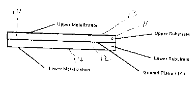
A dual polarized microstrip patch radiator
comprising a ground plane, a thin layer of dielectric on
each side thereof, a conductive microstrip patch on a
first of the dielectric layers on a side remote from the
ground plane, first and second feed lines on the side of
the second dielectric layer remote from the ground
plane, first and second pairs of apertures in the ground
plane the second pair of apertures being orthogonal to
the first pair of apertures, the first feed line being
radiatively coupled to one of the first pair of
apertures and not radiatively coupled to the other
aperture of the first pair of apertures nor to the
second pair of apertures, the second feed line being
radiatively coupled to one of the apertures of the
second pair of apertures and not radiatively coupled to
the other of the second pair of apertures nor to the
first pair of apertures, the other aperture of the first
pair of apertures being positioned to provide a
symmetrical boundary condition for power coupled from
the second feed line, and the other aperture of the
second pair of apertures being positioned to provide a
symmetrical boundary condition for power coupled from
the first feed line, whereby cross-polarization of the
feeds is minimized.
Un réseau rayonnant à microruban à double polarisation comprend un plan de masse, une mince couche de diélectrique de chaque côté de ce dernier, un microruban conducteur sur une première couche diélectrique, du côté éloigné du plan de masse, une première et une deuxième lignes d'alimentation sur le côté de la deuxième couche diélectrique éloigné du plan de masse, une première et une deuxième paires d'ouvertures dans le plan de masse, la deuxième paire d'ouvertures étant perpendiculaire à la première paire d'ouvertures, la première ligne d'alimentation étant couplée par rayonnement à l'une des ouvertures de la première paire d'ouvertures et non couplée par rayonnement à l'autre ouverture de la première paire d'ouvertures ni à la deuxième paire d'ouvertures, la deuxième ligne d'alimentation étant couplée par rayonnement à l'une des ouvertures de la deuxième paire d'ouvertures et non couplée par rayonnement à l'autre ouverture de la deuxième paire d'ouvertures ni à la première paire d'ouvertures, l'autre ouverture de la première paire d'ouvertures étant placée de façon à fournir une frontière symétrique pour la puissance provenant de la deuxième ligne d'alimentation, et l'autre ouverture de la deuxième paire d'ouvertures étant placée de façon à fournir une frontière symétrique pour la puissance provenant de la première ligne d'alimentation, la polarisation croisée des alimentations étant réduite au minimum par ce moyen.
Note: Claims are shown in the official language in which they were submitted.
Note: Descriptions are shown in the official language in which they were submitted.
2024-08-01:As part of the Next Generation Patents (NGP) transition, the Canadian Patents Database (CPD) now contains a more detailed Event History, which replicates the Event Log of our new back-office solution.
Please note that "Inactive:" events refers to events no longer in use in our new back-office solution.
For a clearer understanding of the status of the application/patent presented on this page, the site Disclaimer , as well as the definitions for Patent , Event History , Maintenance Fee and Payment History should be consulted.
| Description | Date |
|---|---|
| Inactive: Adhoc Request Documented | 2018-06-06 |
| Revocation of Agent Requirements Determined Compliant | 2018-05-18 |
| Appointment of Agent Requirements Determined Compliant | 2018-05-18 |
| Inactive: IPC from MCD | 2006-03-12 |
| Time Limit for Reversal Expired | 2002-10-15 |
| Application Not Reinstated by Deadline | 2002-10-15 |
| Deemed Abandoned - Failure to Respond to Maintenance Fee Notice | 2001-10-15 |
| Inactive: Inventor deleted | 2000-06-02 |
| Letter Sent | 1999-05-14 |
| Application Published (Open to Public Inspection) | 1999-04-15 |
| Inactive: Multiple transfers | 1999-03-10 |
| Inactive: IPC assigned | 1998-01-23 |
| Classification Modified | 1998-01-23 |
| Inactive: First IPC assigned | 1998-01-23 |
| Inactive: Filing certificate - No RFE (English) | 1997-12-30 |
| Letter Sent | 1997-12-30 |
| Application Received - Regular National | 1997-12-23 |
| Abandonment Date | Reason | Reinstatement Date |
|---|---|---|
| 2001-10-15 |
The last payment was received on 2000-10-11
Note : If the full payment has not been received on or before the date indicated, a further fee may be required which may be one of the following
Patent fees are adjusted on the 1st of January every year. The amounts above are the current amounts if received by December 31 of the current year.
Please refer to the CIPO
Patent Fees
web page to see all current fee amounts.
| Fee Type | Anniversary Year | Due Date | Paid Date |
|---|---|---|---|
| Application fee - standard | 1997-10-15 | ||
| Registration of a document | 1997-10-15 | ||
| Registration of a document | 1999-03-10 | ||
| MF (application, 2nd anniv.) - standard | 02 | 1999-10-15 | 1999-08-31 |
| MF (application, 3rd anniv.) - standard | 03 | 2000-10-16 | 2000-10-11 |
Note: Records showing the ownership history in alphabetical order.
| Current Owners on Record |
|---|
| CAL CORPORATION |
| EMS TECHNOLOGIES CANADA, LTD. EMS TECHNOLOGIES CANADA, LTEE |
| Past Owners on Record |
|---|
| PETER C. STRICKLAND |

