Note: Descriptions are shown in the official language in which they were submitted.
CA 02218458 2005-O1-28
50336-55
METHOD AND APPARATUS FOR DESIGN VERIFICATION USING EMULATION
AND SIMULATION
Field of the Invention
The present invention relates to combining
emulation and simulation to verify a logic design.
Background of the Invention
Emulation systems proVlde cirCUit and system
designers powerful methods to functionally test out systems
and integrated circuits before committing them to
production. Circuit designers and engineers use emulators
to convert a design into temporary operating hardware, thus
enabling the engineer to test the design at or near real
time conditions. Additionally, the engineer can
concurrently verify the integrated circuits, system hardware
and software. Examples of emulation systems are described
in U.S. Patent Nos. 5,109,353 to Sample et al. and 5,036,473
to Butts et al.
Typically, the design process involves multiple
transformations of a design from the initial design idea
level to the detailed manufacturing level. An engineer may
start with a design idea. The engineer may then generate a
behavioral definition of the design idea. The product of
the behavioral design may be a flow chart or a flow graph.
Next, the engineer may
1
CA 02218458 1998-O1-30
PATENT
220/ 199
design the system data path and may specify the registers and logic units
necessary for
implementation of the system. At this stage, the engineer may establish the
procedure for
controlling the movement of data between registers and logic units through
buses. Logic
design is the next step in the design process whereby the engineer uses
primitive gates and flip-
flops for the implementation of data registers, buses, logic units, and their
controlling
hardware. The result of this design stage is a net(ist of gates and flip-
flops.
The next design stage transforms the netlist of gates and flip-flops into a
transistor list or layout. Thus, gates and flip-flops are replaced with their
transistor equivalents
or library cells. During the cell and transistor selection process, timing and
loading
requirements are taken into consideration. Finally, the design is
manufactured, whereby the
transistor list or layout specification is used to burn fuses of a
programmable device or to
generate masks for integrated circuit fabrication.
Hardware description languages ("HDLs") provide formats for representing the
output of the various design stages described above. These languages can be
used to create
circuits at various levels including gate-level descriptions of functional
blocks and high-level
descriptions of complete systems. Thus, HDLs can describe electronic systems
at many levels
of abstraction.
Hardware description languages are used to describe hardware for the purposes
of simulation, modeling, testing, creation and documentation of designs.
Previously, circuit
designers tended to design at the logic gate level. Increasingly, designers
are designing at
2
CA 02218458 1998-O1-30
PATENT
220/199
higher levels, particularly using HDL methodology. HDLs provide a convenient
format for the
representation of functional and wiring details of designs and may represent
hardware at one
or more levels of abstraction.
Two popular hardware description languages are Verilog and Very-High-Speed
Integrated Circuit (VHSIC) Hardware Description Language ("VHDL"). VHDL began
in the
early 1980s within the United States Department of Defense and it was intended
initially to
be a documentation language for the description of digital hardware systems.
Later, the
language was refined so that descriptions could be simulated and synthesized.
The advent of
HDL-based design tools including design entry, simulation and synthesis has
subsequently
shifted VHDL's focus from design documentation to high-level design. Other
hardware
description languages include, but are not limited to, A Hardware Programming
Language
("AHPL"), Computer Design Language ("CDL"), CONsensus LANguage ("CONLAN"),
Interactive Design Language ("IDL"), Instruction Set Processor Specification
("ISPS"), Test
Generation And Simulation ("TEGAS"), Texas Instrument Hardware Description
Language
("TI-HDL"), Toshiba Description Language ("TDL"), ZEUS, and NDL.
Simulation has long been a preferred method for verification of logical
correctness of complex electronic circuit designs. Simulation is broadly
defined as the creation
of a model which, if subjected to arbitrary stimuli, responds in a similar way
to the
manufactured and tested design. More specifically, the term "simulation" is
typically used
when such a model is implemented as a computer program. In contrast, the term
"emulation"
3
CA 02218458 1998-O1-30
PATENT
220/ 199
is the creation of a model using programmable (also known as reconfigurable)
logic or field-
programmable gate array (FPGA) devices. Simulation saves a significant amount
of time and
financial resources because it enables designers to detect design errors
before the expensive
manufacturing process is undertaken. Moreover, the design process itself can
be viewed as a
sequence of steps where the initial general concept of a new product is being
turned into a
detailed blueprint. Detecting errors at the early stages of this process also
saves time and
engineering resources.
Simulators can be divided into two types. One type of simulator follows
levelized simulation principles, and a second type follows event-driven
simulation principles.
Levelized simulators, at each simulation cycle, have to reevaluate the new
state of every
component of the simulated design, whether or not the input signals of the
component have
changed. Additionally, the component's state has to be retransmitted even if
the state has not
changed. Event-driven simulators only evaluate those components for which some
input
conditions are changing in the current simulation cycle. Consequently, event-
driven simulators
achieve considerable savings in component evaluation time. However,
significant additional
software runtime is spent on the decision-making of whether a particular
component should
be evaluated. As a result, both types of prior simulators (levelized and event-
driven) have
similar performances.
The primary advantage of emulation over simulation is speed. Emulation maps
every component under verification into a physically different programmable
logic device, and
4
CA 02218458 1998-O1-30
PATENT
220/ 199
therefore all such components are verified in parallel. In a typical
simulator, however, the
single processing element serially computes the next state of each component
at every
simulation time step.
Emulation is an efficient verification technology for designs represented as
or
easily converted to a network of logic gates. Modern design methodology,
however, requires
that at the initial design stages, large design portions are represented by
behavioral models.
Through a series of design decisions these behavioral models are gradually
replaced with
equivalent structural representations. Correctness of each replacement step is
subject to
verification, at which point the design presents itself as a complicated mix
of behavioral,
structural, and gate-level components. Structural parts of the design can be
directly mapped
into emulation hardware using widely available logic synthesis programs.
Behavioral portions,
however, can only be compiled into computer programs and executed. By its
nature,
emulation requires creation of a model using actual hardware and therefore
cannot be used
at the early stage of the design cycle when the concept of a new product is
not yet represented
by its components but rather by a high-level description of its functions.
Therefore, to
conduct verification at earlier design stages, the most appropriate
environment would
efficiently combine the features of emulation and behavioral simulation.
Furthermore,
combining emulation and simulation enables a designer to simulate design
components that
cannot be emulated because of physical constraints such as analog signals.
CA 02218458 1998-O1-30
PATENT
220/ 199
As the design approaches completion, emphasis naturally shifts away from
behavioral simulation and towards logic emulation. However, the parts that
represent the
operating environment of the future product may never be converted to a
structural
representation. In this case, the behavioral description of the system-level
environment serves
as a test bench for the emulated design. The system-level behavioral
description generates test
stimulus and evaluates the responses of the design under verification in a way
that closely
replicates the real operating conditions. The need to execute such behavioral
test benches is
another motivation for combining the simulation and the emulation capabilities
in one logic
verification system.
One approach to combining emulation and simulation is to run a simulator on
a host workstation (or network thereof) communicating the events or changes in
signal state
to and from the emulated portion of the design over a network interface.
However, in such
a solution, the speed of event transfer seriously limits performance.
Experiments show that
the average time to transfer a 4-byte data packet over transport control
protocol ( "TCP" )
running on a SUN workstation computer (e.g., a SPARC-20) is around 50
microseconds.
Assuming that a data packet of such size is used for encoding an event and
given average
design activity of 1000 events per simulation cycle, the speed of simulation
will be limited to
20 cycles per second. Therefore, there currently exists a need for combining
emulation and
simulation to efficiently verify circuit designs that may be a mixture of gate-
level, structural and
behavioral representations.
6
CA 02218458 2005-O1-28
50336-55
Summary of the Invention
Accordingly, a general object of the present
invention is to provide an apparatus and method for
efficiently coupling simulation and emulation of a logic
design, so that the overhead of event transfer between the
simulated and the emulated design portions is minimized.
In order to achieve the above object, the design
verification method and apparatus includes at least one
reconfigurable device that is used to emulate a portion of
the logic design under verification. Additionally, at least
one microprocessor is used to simulate another design
portion which may be represented as a behavioral
description. The microprocessor is connected to the
reconfigurable device in a manner that minimizes data
transfer time between the simulated and emulated portions.
Furthermore, an event detector is provided to detect events
during verification of the design. The microprocessor is
relieved from performing such event detection functions,
thereby reducing design verification time.
According to one aspect of the present invention,
there is provided an apparatus for verifying functionality
of a digital logic design using emulation and simulation
comprising: a plurality of programmable logic devices for
emulating a first portion of a design, the programmable
logic devices being programmable to implement digital logic
functions; at least one microprocessor for simulating a
second portion of said design, connected to said plurality
of programmable logic devices so as to minimize time for
transferring data between said first portion of said design
and said second portion of said design; an event detector
connected to said at least one microprocessor for detecting
a plurality of events during design verification, relieving
7
CA 02218458 2005-O1-28
50336-55
said at least one microprocessor from performing event
detection; and a scheduler for scheduling operations that
said at least one microprocessor would ordinarily schedule.
According to another aspect of the present
invention, there is provided an apparatus for verifying
functionality of a digital logic design using emulation and
simulation comprising: a plurality of simulation modules,
each having a microprocessor for simulating a design; a
plurality of programmable logic devices for emulating said
design, connected to said simulation modules, said plurality
of programmable logic devices being programmable such that
digital logic functions can be implemented therein; said
plurality of simulation modules further comprising a
reconfigurable element; said reconfigurable element
comprising an event detector for detecting events to assist
said microprocessors in simulating said design; and a
scheduler for scheduling operations that said microprocessor
would ordinarily schedule.
According to still another aspect of the present
invention, there is provided a method for simulating and
emulating a digital logic design to verify the functionality
of the digital logic design comprising: importing said
design, where a portion of said design is a behavioral
design, to create a behavioral database; dividing said
behavioral design into a plurality of behavioral fragments;
preprocessing said behavioral database to form a
preprocessed behavioral database; generating a plurality of
executables for a plurality of simulation modules for
processing therein; creating a netlist; processing said
netlist to create configuration data for a plurality of
programmable logic devices.
7a
50336-55
CA 02218458 2005-O1-28
According to yet another aspect of the present
invention, there is provided a method for combining
emulation and simulation so that the functionality of a
digital logic design can be verified, comprising:
connecting an emulator and a plurality of microprocessors so
as to minimize time for transferring data between said
emulator and said microprocessors; emulating a first portion
of a design by said emulator; simulating a second portion of
said design by said simulator; detecting a plurality of
events by said emulator that would ordinarily be detected by
said microprocessors, and scheduling a plurality of
operations by said emulator that would ordinarily be
scheduled by said microprocessors.
Additional objects, advantages, and features of
the present invention will further become apparent to
persons skilled in the art from the study of the following
description and drawings.
Brief Description of the Drawings
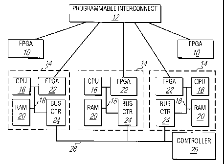
FIG. 1 is a block diagram of one embodiment of a
logic verification system with multiple processors and
programmable gate array devices.
7b
CA 02218458 1998-O1-30
PATENT
220/ 199
FIG. 2 is a block diagram of another embodiment of a logic verification system
which includes a global-event-transfer bus.
FIG. 3 is a block diagram showing the transmission of computed values of
variables from the simulated design portion into the emulated design portion.
FIG. 4 is a block diagram showing the capture of computed values of variables
from the emulated design portion into the simulated design portion.
FIG. 5 is a block diagram showing the computation of event codes and their
transfer to the microprocessor performing behavioral simulation.
FIG. 6 is a block diagram of another embodiment showing the computation of
the event codes and their transfer to the microprocessor performing behavioral
simulation
where events are grouped into, for example, active events, inactive events,
non-blocking assign
update events, and monitor events.
FIG. 7 is a block diagram showing the detection of outstanding events in the
event groups.
FIG. 8 is a block diagram illustrating the computation of a signal that
advances
the simulation time.
FIG. 9 is a block diagram depicting the transfer of the events from one
microprocessor to another over a shared multiplexed bus.
FIG. 10 is a block diagram of an event detector.
8
CA 02218458 1998-O1-30
PATENT
220/ 199
FIG. 1 1 is a block diagram that illustrates one transformation made to the
logic
design under verification to prevent hold-time violations during emulation of
the design.
FIG. 12 is a block diagram that illustrates another transformation made to the
logic design to prevent hold-time violations during the design emulation.
FIG. 13 is a block diagram showing the programming of the logic verification
system.
FIG. 14 illustrates an example of a logic design represented partially by
component interconnection, and partially by behavioral description, using a
code fragment in
Verilog hardware description language.
FIG. 15 illustrates an example of an intermediate representation of the logic
design in the behavioral database (after the completion of the import step 132
shown in FIG.
13).
FIG. 16 illustrates an example of a circuit fragment created by the netlist
generation step 140 (step shown in FIG. 13).
FIG. 17 illustrates an example of executable code (in 'C' programming
language) created by the code generation step 144 (step shown in FIG. 13).
Description of the Preferred Embodiment
FIG. 1 shows the preferred embodiment of the logic verification system. The
system includes one or more reconfigurable logic components which may be
programmable
9
CA 02218458 2005-O1-28
50336-55
gate array ("FPGA") devices 10 interconnected using the
programmable interconnect 12. The interconnect 12 can be
programmed to create an arbitrary connection between any
number of inputs or outputs of the devices connected to it.
The apparatus also includes one or more simulation modules
14 (for exemplary purposes only, three are shown). Each of
the simulation modules 14 includes a microprocessor 16,
connected through a microprocessor bus 18 to one or more
random access memory devices 20, one or more reconfigurable
logic components which may be FPGAs 22, and a system bus
controller 24. Although FIG. 1 only shows one random access
memory device 20, and one FPGA 22, one of skill in the art
would understand that any number of memory devices 20 or
FPGAs 22 could be employed. Furthermore, any type of memory
could be utilized to similarly perform the functions of
random access memory 20. In addition, other types of
reconfigurable logic components such as PALs or PLAs could
perform the function of FPGAs 10, 22. Which type of FPGA to
use is purely a matter of the designer's choice. In the
preferred embodiment, 4036EX devices from Xilinx, Inc. are
used. These devices are described in The Programmable Logic
Data Book from Xilinx dated June 1996, PN 0010303. Which
CPU 16 to use is also purely a matter of the designer's
choice. In the preferred embodiment, the PPC403GC CPU chip
from IBM, Inc. is used. Each of the FPGA devices 22 in each
simulation module 14 is also connected to programmable
interconnect 12.
FPGA devices 10 emulate the logic circuit portions
under verification represented as the interconnection of
components, as disclosed in Butts et al., U.S. Patent No.
CA 02218458 1998-O1-30
PATENT
220/199
5,036,473. Simulation modules 14 simulate the logic circuit portions under
verification
which may be represented by behavioral descriptions. Inside these modules 14,
the
microprocessors 16 selectively execute fragments of the behavioral
description. The hardware
logic implemented in FPGA 22 selects the behavioral fragments to be executed
and the order
of execution. Unlike the event-driven simulators known in the prior art, the
microprocessors
16 are relieved from the functions of detecting, scheduling, and ordering the
events. As a
result, simulation speed is dramatically improved. FPGA devices 22 also
communicate the
signal values shared between the behavioral description portion and those
design portions
represented by the interconnection of components. Additionally, FPGAs 22
communicate
the signal values shared between different simulation modules 14.
It is not integral to the present invention that the FPGA devices 22 do not
emulate logic circuit portions represented as the component interconnections.
Similarly, it is
not integral to the current invention that the FPGA devices 10 do not
implement the logic
that determines the selection and order of the behavioral code fragments for
execution by the
microprocessors 16. Rather, in its preferred embodiment, the present invention
allows for
arbitrary distribution of the hardware logic used for any of these purposes
among the FPGA
devices 10 and the FPGA devices 22. Although for sake of simplicity FPGA
devices 22 are
employed, it is understood to one of skill in the art that the FPGA devices 10
could be
similarly employed.
CA 02218458 1998-O1-30
PATENT
220/ 199
The system bus controllers 24 are connected to the system controller 26
through the system bus 28. The system controller 26 performs the functions of
downloading
configuration data into the FPGA devices 10, 22, downloading the executable
data into the
random access memory devices 20, starting the logic verification system,
communicating data
between the logic verification system and the host workstation (not shown).
The system
controller 26 is implemented using a commercial embedded controller board or
by any other
means known to those skilled in the art.
Random access memory devices 20 store the behavioral code fragments, and
the values of the simulation variables that are not shared between the
behavioral description
portions and the component interconnection portions, or between multiple
simulation modules
14. System bus controllers 24 communicate data to and from the system
controller 26
through the system bus 28. The logic verification system permits programming
of
configuration data for the FPGA devices 10, 22 and programmable interconnect
12. Also,
executable software code fragments are downloaded into the random access
memory devices
20. Such programming may be implemented as a computer program and executed on
a
computer workstation.
An alternative embodiment of the logic verification system is shown in F1G. 2.
This embodiment further includes a global-event-communication bus that
comprises a plurality
of signal lines 30 connected in parallel to all FPGA devices 22, and a daisy
chain line 32 that
connects all FPGA devices 22 serially. Note that this embodiment would also
include system
12
CA 02218458 1998-O1-30
PATENT
220/ 199
bus controllers 24, a system controller 26 and a system bus 28 as shown in
FIG. 1. These
components are omitted in FIG. 2 to simplify the drawing. The global-event-
communication
bus is included because the programmable interconnect 12 constitutes a limited
and expensive
resource. Rather than routing the signals shared between the multiple
simulation modules 14
through programmable interconnect 12, such signals can be communicated in a
serial fashion,
one signal at a time, over the global-event-communication bus. The simulation
module 14,
that serves as a transmitter of a new signal value, sets some of the signal
lines 30 to represent
the serial number of such signal and its new value. This information reaches
all other
simulation modules 14 and is captured as necessary.
In the case where several simulation modules 14 serve as transmitters at the
same time, the order needs to be imposed in which they take control of the
signal lines 30.
To accomplish this ordering, the daisy chain line 32 is operated according to
the token ring
principle. At any given moment a token represented by a value on the input
portion of daisy
chain line 32 resides with one of the simulation modules 14, giving that
module 14 the right
to control the signal lines 30. After finishing its transmission, the
simulation module 14
surrenders the token to the next module along the daisy chain line 32 and so
on.
In addition to transmitting the signals shared between simulation modules 14,
the global-event-communication bus also transmits the signals that synchronize
the operation
of simulation modules 14. Examples of such synchronization signals include the
simulation
13
CA 02218458 1998-O1-30
PATENT
220/ 199
time advancement signal, and the BUSY signals indicating that the simulation
modules 14 still
have some number of events to be processed in the current simulation cycle.
While executing the behavioral description fragments, the microprocessors 16
need to set the new values to the variables that describe the current state of
the logic design
being simulated. Those variables that are locally used in only one simulation
module 14 are
represented by appropriate locations in the random access memory device 20.
Those variables, however, that are shared between the behavioral description
portions and component interconnection portions, and those that are shared
between multiple
simulation modules 14 must be transmitted outside of a simulation module 14.
FIG. 3
illustrates such transmission where the microprocessor bus 18 is split into a
plurality of address
lines 34, a bus operation (read or write) line 36, a plurality of data lines
38 representing the
code that uniquely identifies the variable being transmitted (also known as
"variable ID"), and
the data line 40 representing the new value of such variable. Upon execution
of an i/o
instruction, the microprocessor 16 installs appropriate signal values on lines
34 through 40
which together constitute the microprocessor bus 18. A certain unique
combination of values
on lines 34 and 36 indicates to the operation decoder 42 that the
microprocessor 16 will
transmit a new value of some variable. In response, the operation decoder 42
enables the
variable selector 44 which then recognizes the combination of values on lines
38 as indicative
of a particular variable. In response, the variable selector 44 enables the
register 46 that
captures the new variable value from the line 40.
14
CA 02218458 1998-O1-30
PATENT
220/ 199
Similarly, in the course of executing the behavioral description fragments the
microprocessors 16 need to capture the new variable values that describe the
current state of
the logic design being simulated. Those variables that are focally used in
only one simulation
module 14 are represented by appropriate locations in the random access memory
device 20.
Those variables that are shared between the behavioral description portions
and the
component interconnection portions, and those shared between multiple
simulation modules
14 must be captured from outside of the simulation module 14. FIG. 4
illustrates such
capture where FPGA 22 additionally includes a multiplexer 48, an intermediate
register 50,
and a bus driver 52.
The capture operation proceeds in two steps and takes two microprocessor
instructions to complete. In the first step a write operation is performed.
The operation
decoder 42 recognizes a combination of an address on lines 34 and a bus
operation on line
36 as indicative of the microprocessor's intent to start the capture of a
variable value. In
response, the operation decoder 42 enables a register 50 which in turn
captures the variable
value selected by the multiplexer 48 based on the variable ID on lines 38.
In the second step a read operation is performed. The operation decoder 42
recognizes a combination of an address on lines 34 and a bus operation on line
36 as
indicative of the microprocessor's intent to complete the capture of a
variable value. Next,
the operation decoder 42 enables a bus driver 52 that transmits the variable
value from the
output of register 50 and onto the line 40 of the microprocessor bus 18.
CA 02218458 1998-O1-30
PATENT
220/ 199
As discussed earlier, the hardware logic implemented in FPGAs 10 and 22
select and order the behavioral code fragments for execution by the
microprocessors 16. One
embodiment of such logic is shown in FIG. 5. The embodiment contains one or
more event
detectors 54 (for exemplary purposes, two are shown), an event encoder 56, and
a bus driver
58. Each event detector 54 independently produces a signal that triggers the
execution of one
particular fragment of behavioral code by the microprocessor 16. That signal
is fed into an
event encoder 56 that provides a code (known as an "event ID") at its output
that uniquely
identifies its input signal that has been set.
If two or more inputs to the event encoder 56 are set at the same time, it
produces the ID of the event that has preference in the behavioral code
fragments execution
order. For example, it could be the event which has a smaller event ID value.
When the microprocessor 1 fi is ready for execution of the next behavioral
fragment, it performs a read operation. The operation decoder 42 recognizes a
combination
of an address on lines 34 and a bus operation on line 36 as indicative of the
intent of the
microprocessor to capture the ID of the next behavioral code fragment to be
executed. In
response, the operation decoder enables a bus driver 58 that transmits the
event ID from the
output of event encoder 56 onto the lines 38 of the microprocessor bus 18.
When none of
the event detectors 54 produce a signal requesting the execution of a
behavioral code
fragment, the event encoder 56 produces an output signal indicating to the
microprocessor
16 that no operation is required at this time. The appearance of the output
signal at the
16
CA 02218458 1998-O1-30
PATENT
220/ 199
output of at least one of the event detectors 54 can, in one embodiment, cause
an interrupt
operation of the microprocessor 16.
After transmitting the event ID to the microprocessor 16, the event encoder 56
automatically resets the corresponding event detector 54. The reset circuit is
not shown in
the drawings but is well known in the art, and can be readily reproduced by
one skilled in the
art.
Another embodiment of the event ID computation logic is shown in FIG. 6. In
this embodiment the event detectors 54 are grouped according to scheduling
requirements
of the behavioral model. For example, for models written in Verilog hardware
description
language such requirements are defined by chapter 5 of the LE.E.E. Draft
Standard 1364.
Particularly, Verilog models require that all events processed in the same
simulation cycle be
grouped into four groups, namely the active events, the inactive events, the
non-blocking-
assign-update events, and the monitor events. Verilog models further require
that any active
events are processed before any inactive events which in turn are processed
before any non-
blocking-assign-update events which in turn are processed before any monitor
events.
To conform to these requirements, the embodiment shown in FIG. 6 comprises
a plurality of groups of event detectors. Each group has one or more event
detectors 54 (for
example, one is shown in each group) and an AND gate 60, except that the first
group does
not contain such AND gate 60. The AND gate 60 that belongs to the second group
is
controlled by BUSY[ 1 ] signal 62a indicating there are unprocessed events in
the first group.
17
CA 02218458 1998-O1-30
PATENT
220/ 199
Similarly, the AND gate 60 of the third group is controlled by BUSY[ 1 ]
signal 62a and by
BUSY[2] signal 62b, the latter indicating that there are still unprocessed
events in the second
group. As a result, the signal from an event detector 54a that belongs to the
second group
will reach event encoder 56 only if there are no outstanding events in the
first group.
Similarly, the signal from an event detector 54b that belongs to the third
group will reach
event encoder 56 only if there are no outstanding events in the first or the
second groups.
The pattern continues for the fourth and further groups utilizing more of the
BUSY signals 62
as necessary.
The formation of the BUSY signals 62 is shown in FIG. 7. Each BUSY signal
62 is formed as a logic OR function 64 of the output signals of all event
detectors 54 that
belong to the corresponding group. Specifically, BUSY[ 1 ] signal 62a is
formed using the
event detectors of the first group, BUSY[2] signal 62b is formed using the
event detectors of
the second group, and so on. It has to be appreciated that outputs from all
event detectors
54 within a group from all simulation modules 14 must be OR'ed together to
form a BUSY
signal 62. In one embodiment of the present invention, wired logic is used to
form a BUSY
signal 62, so that the OR function 64 is implicitly implemented as a wire. In
yet another
embodiment, some of the global-event-communication bus lines 30 are used to
propagate the
BUSY signals 62 among all of the simulation modules 14.
When none of the BUSY signals 62 are asserted, the current simulation cycle
is completed. The circuit that detects such completion and advances the
simulation to the
18
CA 02218458 1998-O1-30
PATENT
220/ 199
next cycle is shown in FIG. 8. It consists of a NOR gate 66 with the number of
inputs
corresponding to the number of BUSY signals 62 used, and the counter 68.
Although four
BUSY signals 62 are shown as the inputs to NOR 66, it is understood that any
number of
BUSY signals 62 can be employed. When none of the BUSY signals is asserted the
NOR gate
66 enables the operation of the counter 68. The counter is clocked by a fast
periodic clock
signal 70 that runs asynchronously and continuously inside the logic
verification system. The
frequency of this clock should be higher than the frequency of the signal
transitions in the
system. After counting the number of clock cycles on clock signal 70 necessary
to
compensate for the longest propagation delay of BUSY signals 62, the counter
68 overflows
producing time advance signal 72 that is propagated to all of the simulation
modules 14. In
one embodiment of the present invention, global-event-communication bus lines
30 are used
to propagate the time advance signal among all of the simulation modules 14.
FIG. 9 details the transferring of the events from one FPGA 22 to another over
a shared multiplexed bus 82. This method of data transfer is used in one
embodiment of the
present invention in order to conserve the valuable resources of the
programmable
interconnect 12.
The transmitting FPGA 22 (shown on the left of FIG. 9) includes a second
event encoder 74 similar in its functionality to the event encoder 56. The
transmitting FPGA
22 further includes the bus driver 76 (which is similar to the bus driver 58)
and the transmit
controller 78. When the transmit controller 78 detects the bus arbitration
input signal 80,
19
CA 02218458 1998-O1-30
PATENT
220/ 199
it checks if the event encoder 74 has any active signals at its inputs coming
from a plurality
of event detectors 54. If such signals exist, it enables the transmission of
the first event ID
through bus driver 76 and onto the shared multiplexed bus 82. After a number
of cycles of
the fast periodic clock signal 70 (not shown) necessary to compensate for the
longest
propagation delay of bus 82, transmit controller 78 signals event encoder 74
to reset the
event detector 54 corresponding to the event already transmitted, and to bring
up the next
event in a predefined order. After transmitting all events, the transmit
controller 78 disables
the bus driver 76 and asserts the bus arbitration output signal 84, thus
relinquishing control
over the bus 82. Bus arbitration output signal 84 of one simulation module 14
is connected
to bus arbitration input signal 80 of another simulation module 14 to form a
daisy chain.
In the receiving FPGA 22 (shown on the right of FIG. 9), the shared
multiplexed bus 82 splits into event ID lines 88, variable value line 86, and
event ready line
90. On detection of an event ready signal 90, a variable selector 92
recognizes the
combination of values on lines 88 as indicative of a particular variable. In
response, the
variable selector 92 enables the register 46 that captures the new value of
the variable from
the line 86.
In one embodiment of the present invention, global-event-communication bus
lines 30 are used to implement the shared multiplexed bus 82 and sections of
the daisy chain
32 are used to implement the bus arbitration signals 80 and 84.
CA 02218458 1998-O1-30
PATENT
220/ 199
FIG. 10 details the preferred embodiment of the event detector 54. It includes
a combinational logic block 98 with one or more inputs and one output. One or
more of the
inputs of the block 98 may be connected directly to the signals that represent
the variable
values. Other inputs of the block 98 may be connected to the signals that
represent the
variable values through other combinational blocks 94 and edge detectors 96.
The edge
detectors 96 detect the positive edge, the negative edge, or any edge of their
input signals.
The construction of edge detector is not shown but could be readily reproduced
by one of skill
in the art, and is well known in the art.
As shown in FIG. 10, the output of combinational block 98 is connected to the
"Set" input of flip/flop 102 directly or through the delay counter 100. In the
latter case, the
output signal of the combinational logic block 98 enables the delay counter
100 which is
clocked by a time advance signal 72. After counting the predetermined number
of time
advance signals 72, the counter 100 overflows and produces the signal at the
output of event
detector 54. After the event output has been transmitted, event detector 54 is
reset using
the reset line 1 O1 by event encoder 56 as explained previously.
The general structure shown in FIG. 10 can implement an arbitrary level
sensitive event control (using only combinations) logic block 98), or edge
sensitive event
control (also using the combinational blocks 94 and edge detectors 96), or
delay (also using
the delay counter 100), or any combination thereof. Each particular event
detector 54 can
have all or only a portion of those capabilities, as needed.
21
CA 02218458 1998-O1-30
PATENT
220/ 199
Emulation technology in general is not appropriate for verification of the
actual
timing of the design in the sense of computing the accurate time intervals
between various
input and output signal events. Correct model timing is important, therefore,
only as a
method of ensuring the correct evaluation order of different circuit
components which have
data dependencies on each other. The most important case of this timing
correctness problem
is the evaluation of chains of flip/flops with possible hold-time violations.
There is a specified
"setup time" and "hold-time" for any clocked device. Setup time requires that
input data
must be present at the data input lead of a flip-flop device and in stable
form for a
predetermined amount of time before the clock transition. Hold-time requires
that the data
be stable from the time of the clock transition on arrival at the control lead
of a flip-flop up
to a certain time interval after the arrival of the clock for proper
operation. A key process in
implementing a logic circuit from a user's netlist is to synchronize the setup
and hold-time of
data with the arrival of a corresponding clock. Data must be present and
stable at the D input
of a flip-flop for a specific space of time with respect to the arrival of the
corresponding clock
at the clock input to ensure the proper operation of the implemented logic
circuit. In
implementing a circuit from a user's netlist, the proper timing of clock
signals may be hindered
due to excessive delay in the clock lines by reason of clock skew. This may
cause data in a first
logic device such as a flip-flop or shift register to shift earlier than data
on second register. The
hold-time requirement of the second register is violated and data bits may
then be lost unless
the shift registers are properly synchronized.
22
CA 02218458 1998-O1-30
PATENT
220/ 199
Hold-time violations may not occur in the target system or end product because
the violation is an artifact of emulation circuits. This is because hold-time
violations result from
clock skews in the emulation circuit that are frequently different from clock
skews in the target
system, since limited resources in reprogrammable logic devices are designed
to support the
generation of clock signals. Since behavioral simulation in the logic
verification system requires
co-existence of the simulated and the emulated circuit components, it is
important that
compatible means are used for timing correctness in both technologies.
In simulation technology, model timing is described by the appropriate
language
constructs such as delays and non-blocking assignment statements. Timing is
correct by
definition as long as the semantics of such constructs are correctly
interpreted by the simulator.
This is true even in the case of zero-delay simulation when the actual delay
values are
presumed unknown. For example, two flip/flops could each be defined by the
following
behavioral code in Verilog hardware description language which will ensure
correct order of
evaluation:
always @ (posedge clk)
q = #0 d;
or
always @ (posedge clk)
q < = d;
23
CA 02218458 1998-O1-30
PATENT
220/ 199
The interpretation of explicit delays, zero delays, and non-blocking
assignments is based on
assigning the events to different simulation cycles or to different groups in
the same cycle.
These event assignments enforce the event order implied by language semantics
for the
behavioral design portion.
In emulation technology, however, the pair of serially connected flip/flops
are
described as:
always @ (posedge clkl )
ql = #tl dl;
always @ (posedge clk2)
q2 = #t2 d2;
assign #td d2 = q 1;
assign #tc clk2 = clkl;
(All emulation circuit delays tl, t2, td, and tc are unknown but have an upper
bound T.) In
order to ensure correct evaluation order, the emulator artificially increases
the value of td by
T. The emulator also performs circuit transformations (such as separation of
the common part
of the clock tree into a special FPGA device and duplication of the clock
logic) so that the
value of T is as small as possible. This process is explained in U.S. Patent
No. 5,475,830,
"Structure and Method for Providing a Reconfigurable Emulation Circuit without
Hold Time
Violations," issued on December 12, 1995 to Chen et al. (assigned to Quickturn
Systems,
Inc.).
24
CA 02218458 1998-O1-30
PATENT
220/199
Each approach to ensuring timing correctness is consistent within its own
domain. However, mixing emulation and simulation model timing together may
create a
problem. Consider for example, the possibility that the second flip/flop in a
chain, or any part
of its clock logic, is described as zero-delay behavior (i.e., a simulation
model) rather than as
an emulation model. In this case the upper bound T of the delay values cannot
be determined
and the method of ensuring timing correctness used by a typical emulator will
not work.
One solution to eliminate hold-time violations places an additional flip/flop
upstream along the datapath of each emulation flip/flop. An example of this
approach is
shown in U.S. Patent No. 5,259,006, "Method for Substantially Eliminating Hold
Time
Violations in Implementing High Speed Logic Circuits or the like," issued on
November 2,
1993 to Price et al., (assigned to Quickturn Systems, Inc.). However, this
solution is difficult
or impossible to apply in a behavioral verification system because it would
require each
behavioral block to be classified as either flip/flop or a combinational
circuit in order to
determine if an additional flip/flop needs to be inserted. It would also be
necessary to identify
each input of such block as a data input or clock input. Such identification
is difficult or
impossible because of hardware description language constraints. If an
additional flip/flop is
placed upstream of a combinational logic block it can alter the behavior
intended by the
designer.
One solution offered by the present invention is a different kind of delay-
independent hold-time violation elimination. As shown in FIG. 1 1, for every
emulation
CA 02218458 1998-O1-30
PATENT
220/ 199
flip/flop 104 that is a source of a signal that could potentially reach any
other circuit
component 106 with a hold-time violation, an additional flip/flop 108 is
inserted downstream.
The simulation clock 1 10 is asserted at the time all of the BUSY signals 62
are deasserted.
As a result, the effective delay in the datapath 112 stemming from the
flip/flop 104 is always
larger than any delay in a combinational clock path 1 14 separating clock
signal 1 16 of
flip/flop 104 and clock signal 118 of flip/flop 1 O6, no matter if flip/flop
104 is emulated or
simulated.
A more complicated situation is shown in F1G. 12 where an emulated flip/flop
120 exists in a clock circuit 122. Assuming that the design intent was that
the delay of circuit
122 is less than the delay of circuit 112, an additional flip/flop should not
be inserted in clock
circuit 122. If the signal produced by such flip/flop 120 is also used as data
source for
another flip/flop 126 then the addition of flip/flop 124 and duplication of
circuit 122 as
circuit 128 is necessary as shown in FIG. 12. Signal 130 previously connecting
circuit 122
with flip/flop 126 should be eliminated. For these transformations to be
applied correctly,
clock circuit analysis needs to be performed that will determine which clock
edges could
potentially be active on the clock inputs of every storage element (either
emulated or
simulated). For behavioral blocks, conservative assumptions as to their
storage capability may
be applied because, even if an extra flip/flop is erroneously identified as
posing the danger of
hold-time violation, the transformation will not alter the function performed
by the circuit
26
CA 02218458 1998-O1-30
PATENT
220/ 199
under verification. In the worst case every flip/flop in the emulated portion
of the circuit will
have to be duplicated with a flip/flop synchronized by the simulation clock
signal 1 10.
FIG. 13 shows a flow diagram for preparing configuration data to be used by
the logic verification system. In general, the compilation starts from the
user's design
description file in, for example, Verilog hardware description language
("Verilog HDL").
However, the compilation could start with a variety of other languages. As a
result of an
import step 132, the behavioral database representation 134 is created. This
representation
is augmented by preprocessing step 136 resulting in another behavioral
representation 138.
Netlist generation step 140 and code generation step 144 result in a netlist
representation of
an emulation model 142 and a set of executables 146 downloadable into logic
module
processor memories 20. The netlist representation 142 is subjected to
partitioning,
placement, and routing step 148 which produces the configuration data 150 for
FPGAs 10,
22 and programmable interconnect 12. The partition, placement and routing step
is
described in U.S. Patent Nos. 5,329,470 to Sample et al. and 5,036,473 to
Butts et al. and
is well known to one skilled in the art.
More specifically, the importer 132 processes the user's Verilog source files
and
produces a behavioral database library. It accepts a list of source file
names, "include" paths,
and a list of search libraries where the otherwise undefined module references
are resolved.
The importer divides the behavioral description into a set of concurrently
executable code
fragments.
27
CA 02218458 1998-O1-30
PATENT
220/199
The preprocessor 136 transforms the behavioral database library created by
import step 132. It partitions the behavioral code into clusters directed for
an execution on
each of the available simulation modules 14, determines the execution order of
the behavioral
code fragments, and the locality of variables in the partitions. Also, the
preprocessor 136
performs transformations necessary for the creation of a hold-time-violation-
free model as
described above.
The code generator 144 reads the behavioral database library as transformed
by the preprocessor 136 and produces downloadable executables 146 for each of
the
simulation modules 14 as identified by the preprocessor 136.
The netlist generator 140 reads the behavioral database library as transformed
by the preprocessor 136 and produces a netlist database library for further
processing by the
partitioning, placement, and routing step 148.
The operation of the logic verification system is based on the principles of
event-
driven simulation which are well known to one skilled in the art. The basic
assumptions are
as follows: ( 1 ) Any given behavioral model can be divided into a set of
evaluation procedures,
which are compiled based on behavioral descriptions; (2) the process of
simulation consists
of a series of executions of these procedures in which they read the logic
values of some
variables (inputs) and compute the new values of some other variables
(outputs); and (3) the
procedures are assigned triggering conditions which define whether or not to
execute each
procedure depending on the current state of the simulation model.
28
CA 02218458 1998-O1-30
PATENT
220/ 199
For example, consider the Verilog HDL model shown in FIG. 14. This model
consists of 10 evaluation procedures, starting with Q AN02. Nine of these
procedures are
predefined by reference to the library primitives Q AN02 and Q FDPO and one is
represented with a behavioral description. The relationship between evaluation
procedures can
be described by a graph as shown in FIG. 15.
For purposes of emulation, instances U 1 and m0 - m7 can be directly
implemented in a FPGA. Behavioral code that evaluates the outputs of instance
line select can
be compiled as a sequence of instructions for an embedded microprocessor. In
order for this
sequence to be invoked at the appropriate time, an unique ID has to be
assigned to each such
sequence loaded into one microprocessor. The ID can be generated in an FPGA
when the
corresponding triggering condition becomes true. (The circuitry for generating
IDs was
previously described in FIG. 5.) If several triggering conditions become true
at the same time,
the smallest of their IDs is generated. The microprocessor 16 continuously
monitors the IDs
and each time a new ID is generated, the corresponding instruction sequence is
executed.
Assuming that the 1D of line select function is 5, the event-generating logic
could be
implemented as shown in FIG. 16. When the negative edge of CLK is detected
(synchronized
by a fast periodic signal) it sets an RS-trigger in an event detector 152. If
there are no events
with IDs less than 5, then the event encoder 154 generates the number 5 and
the
microprocessor 16 detects the number 5 when a read instruction is executed
from one of the
29
CA 02218458 1998-O1-30
PATENT
220/199
addresses that belong to FPGA address space. At this time RS-trigger is reset.
(The operation
decoder, bus drivers and data register are not shown.)
The operation method can be summarized as follows. At model compile time
the cells represented with behavioral code (e.g., line select cell in FIG. 15)
are replaced with
their corresponding event generation logic blocks (similar to the one shown in
FIG. 16.) At
execution time, the microprocessor 16 is continuously running in a loop that
consists of
reading the ID of the next event from the FPGA, and executing a function
corresponding to
this event. An example of a program that could be used by microprocessor 16 to
perform
this operation is shown in FIG. 17.
This software-hardware implementation of a simulation algorithm combines the
best features of levelized and event-driven simulation. As in event-driven
simulation, only
those primitives are evaluated at each cycle for which the activation
conditions are satisfied.
As in Ievelized compiled simulation, the overhead of event queue manipulation
is removed
from the model execution phase. All necessary event detection and manipulation
is done in
reconfigurable hardware (FPGAs). The event-detection hardware netlist is
generated at
compile time based on the triggering conditions for each evaluated routine, as
well as the
results of model partitioning and sorting.
While a presently-preferred embodiment of the invention has been disclosed, it
will be obvious to those skilled in the art that numerous changes may be made
without
departing from the spirit or scope of the invention. It is intended that all
matter contained in
CA 02218458 1998-O1-30
PATENT
220/ 199
the above description and shown in the accompanying drawings shall be
interpreted as being
illustrative and not limiting. The invention, therefore, is not to be limited
except in
accordance with the below claims.
31