Language selection

Search

Patent 2218751 Summary

Third-party information liability

Some of the information on this Web page has been provided by external sources. The Government of Canada is not responsible for the accuracy, reliability or currency of the information supplied by external sources. Users wishing to rely upon this information should consult directly with the source of the information. Content provided by external sources is not subject to official languages, privacy and accessibility requirements.

Claims and Abstract availability

Any discrepancies in the text and image of the Claims and Abstract are due to differing posting times. Text of the Claims and Abstract are posted:

  • At the time the application is open to public inspection;
  • At the time of issue of the patent (grant).
(12) Patent: (11) CA 2218751
(54) English Title: A SILICON SUBSTRATE HAVING A RECESS FOR RECEIVING AN ELEMENT, AND A METHOD OF PRODUCING SUCH A RECESS
(54) French Title: SUBSTRAT DE SILICIUM POURVU D'UNE RAINURE RECEPTIONNANT UN ELEMENT ET PROCEDE DE FABRICATION DE CETTE RAINURE
Status: Term Expired - Post Grant Beyond Limit
Bibliographic Data
(51) International Patent Classification (IPC):
  • G02B 06/36 (2006.01)
  • G02B 06/42 (2006.01)
(72) Inventors :
  • BACKLUND, YLVA (Sweden)
(73) Owners :
  • TELEFONAKTIEBOLAGET LM ERICSSON (PUBL)
  • TELEFONAKTIEBOLAGET LM ERICSSON
(71) Applicants :
  • TELEFONAKTIEBOLAGET LM ERICSSON (PUBL) (Sweden)
  • TELEFONAKTIEBOLAGET LM ERICSSON (Sweden)
(74) Agent: ERICSSON CANADA PATENT GROUP
(74) Associate agent:
(45) Issued: 2008-06-17
(86) PCT Filing Date: 1996-04-23
(87) Open to Public Inspection: 1996-10-31
Examination requested: 2003-03-21
Availability of licence: N/A
Dedicated to the Public: N/A
(25) Language of filing: English

Patent Cooperation Treaty (PCT): Yes
(86) PCT Filing Number: PCT/SE1996/000531
(87) International Publication Number: SE1996000531
(85) National Entry: 1997-10-21

(30) Application Priority Data:
Application No. Country/Territory Date
9501591-3 (Sweden) 1995-04-27

Abstracts

English Abstract


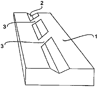
In a silicon substrate (1) having a recess (2) for receiving an element, at
least one holding element (3), integral with the substrate,
extends, at least partly, over the recess (2) to hold an element received in
the recess (2) in place.


French Abstract

Un substrat de silicium (1), comportant une rainure (2) destinée à réceptionner un élément, se caractérise en ce qu'au moins un élément de retenue (3) intégré s'étend, au moins partiellement, au-dessus de l'évidement (2) afin de retenir un élément réceptionné dans cet évidement (2).

Claims

Note: Claims are shown in the official language in which they were submitted.


6
1. A silicon substrate having a groove with a length in its
longitudinal direction for receiving an element and at
least one holding element, which are formed integral with
the substrate and have an extension in the longitudinal
direction of the groove which is less than the length of
the groove the silicon substrate being characterized in
that the holding element are in the form of tongues which
extends partly over the groove alternately from each side
of the groove, to hold an element received in the groove in
place.
2. A silicone substrate according to claim 1, characterized
in that said the holding elements extend completely across
the groove.
3. A method of producing a groove having a length in its
longitudinal direction in a silicon substrate for receiving
an element, comprising masking areas on the substrate on
either side of the intended groove and thereafter etching
out the groove masking also areas on the substrate, which
are of an extension in the longitudinal direction of the
intended groove and extend over the intended groove
alternately from each side of the groove to etch out
holding elements in the form of tongues corresponding to
the areas for holding an element received in the groove in
place.
4. A method according to claim 3, in which the substrate is
of a first doping type, characterized in that the masking

7
is produced by doping the substrate in said areas with a
dopant of a second doping type.
5. A method according to claim 4, characterized in that
said areas on the substrate, which partly extend over the
intended groove are doped to a depth corresponding to the
desired thickness of the holding elements.

Description

Note: Descriptions are shown in the official language in which they were submitted.


CA 02218751 1997-10-21
WO 96134305 PCT/SE96/00531
1
A silicon substrate having a recess for receiving an element,
and a method of producing such a recess
TECHNICAL FIELD
The invention relates to a silicon substrate having a recess
for receiving an element as well as to a method of producing
a recess in a silicon substrate for receiving an element,
comprising masking areas on the substrate on either side of
the intended recess, and thereafter etching out the recess.
BACKGROUND OF THE INVENTION
It is generally known within the opto-electronic field to
exactly align optical fibres with a high grade of accuracy by
receiving the fibres in etched out grooves, so called V-groo-
ves, in silicon substrates.
However, when mounting the optical fibres in such grooves, it
can be difficult to make the optical fibres stay in place in
the respective groove during all of the mounting operation.
When gluing the optical fibres to the grooves, it has, more-
over, loeen observed that the optical fibres will rise some-
what in the grooves due to the thickness of the glue layer,
and, consequently, the position of the respective optical
fibre in the vertical direction as well as the lateral direc-
tion on the substrate will be indefinite.
BRIEF DISCLOSURE OF THE INVENTION
The general object of the invention is to bring about a
simple holding element for elements which are received in
recesses in silicon substrates.
This is attained in the substrate according to the invention
in tha=t at least one holding element integral with the sub-
strate, extepds at least partially over the recess to hold an
elemen't received in the recess in place.
The me'thod according to the invention of producing a recess
in a silicon substrate is mainly characterized by masking

CA 02218751 1997-10-21
WO 96/34305 PCT/SE96100531
2
also at least one area on the substrate, which, at least par-
tly, extends across the intended recess to etch out a holding
element corresponding to that area for holding an element
received in the recess in place.
BRIEF DESCRIPTION OF THE DRAWING The invention will be described more in
detail below with
reference to the appended drawing on which
Fig. 1 is a perspective view of a silicon substrate having a
recess in the form of a V-groove with a first embodiment of a
holding element according to the invention,
Fig. 2 is a schematical plan view of a section of a silicon
substrate having a recess in the form of a V-groove with a
second embodiment of a holding element according to the in-
vention and
Fig. 3 is a schematical plan view of a section of a silicon
substrate having a recess in the form of a V-groove with a
third embodiment of the holding element according to the in-
vention.
PREFERRED EMBODIMENTS
Fig. 1 is a perspective view of a silicon substrate 1 having
a recess in the form of a V-groove 2 for receiving an element
(not shown), e.g. an optical fibre to be aligned relative to
another element (not shown), two optical fibres to be spli-
ced, a shaft to be rotated, a piston rod to be displaced back
and forth in the groove etc. It is to be understood that a
plurality of such grooves may be present on one and the same
substate.
Such a groove 2 is produced in that the silicon substrate 1,
which is of a first doping type (n type or p type), is doped
on either side of the intended groove 2 with a dopant of a
second doping type (p type and n type, respectively), whereu-
pon the intended groove 2 is etched in a manner known per se.

CA 02218751 1997-10-21
WO 96/34305 PCTJSE96I00531
3
In this connection, it should be pointed out that the
recesses do not necessarily have to be V-type grooves, but
the recesses may be of any form in order to be able to recei-
ve e.g. electric components in the form of semiconductor
chips.
In the embodiment of the invention shown in Fig. 1, two hol-
ding elements 3, which are formed integral with the substrate
1, extend obliquely across the groove 2, forming bridges,
which are intended to keep e.g. an optical fibre (not shown)
received in the groove 2 in place alternatively to keep one
optical fibre each in place in connection with e.g. a fibre
splicing operation.
The ho:Lding elements or bridges 3 shown in Fig. 1, are pro-
duced in accordance with a first embodiment of the method
according to the invention in that areas on the substrate 1
corresponding to the bridges 3, are also doped with the above
dopant of said second doping type, whereupon the bridges 3
are etched out in connection with the etching out of the gro-
ove 2.
The bridges 3 do not necessarily have to be of one and the
same width but can actually be of any form.
It should be pointed out that bridges which extend perpendi-
cularly across the groove can not be etched out on (100)-ori-
ented silicon, but a certain, predetermined relationship has
to exist between the form of the bridges and the angle of the
bridges to the upper lateral edges of the groove on the sub-
strate in order for the bridges to be formed upon etching.
The thickness of the bridges 3 is dependent on how deep the
substrate 1 has been doped within the areas which are to form
the bridges 3.
Fig. 2 is a schematical plan view of a section of a substrate
1' having a groove 2' and a holding element 4 in the form of
a tongue which extends from the left side of the groove 2'

CA 02218751 1997-10-21
WO 96/34305 PCT/SE96/00531
4
out over the groove 2' to a distance which in the embodiment
shown corresponds to less than half the width of the groove
2'.
In this connection, it should be pointed out that holding
elements which do not completely extend across the groove,
.
very well can be perpendicular to the edge of the groove.
Also Fig. 3 is a schematical plan view of a section of a sub-
strate 1" having a groove 2" and a couple of holding elements
5 in the form of tongues which from either side of the groove
2" extend perpendicularly over the groove to a distance which
in the embodiment shown corresponds to a little more than
half the width of the groove 2".
The tongues in Figs. 2 and 3 may be produced with such a
thickness that a certain flexibility is obtained so that they
can be lifted upwards manually in order to be able to place
an element of some kind to be held in the groove.
Thus, the holding elements according to the invention are
formed integral with the substrate in the manner described
above in connection with the etching of the grooves and/or
recesses in the substrate, and can in a simple manner be pro-
duced with a desired thickness to keep optical fibres or
other elements in place.
In the embodiment of the method according to the invention
described above, it is possible to produce bridges of such a
thickness and flexibility that they can be manually depressed
to snap into contact with an element thereunder to further
improve the holding action.

Representative Drawing
A single figure which represents the drawing illustrating the invention.
Administrative Status

2024-08-01:As part of the Next Generation Patents (NGP) transition, the Canadian Patents Database (CPD) now contains a more detailed Event History, which replicates the Event Log of our new back-office solution.

Please note that "Inactive:" events refers to events no longer in use in our new back-office solution.

For a clearer understanding of the status of the application/patent presented on this page, the site Disclaimer , as well as the definitions for Patent , Event History , Maintenance Fee  and Payment History  should be consulted.

Event History

Description Date
Inactive: Expired (new Act pat) 2016-04-23
Grant by Issuance 2008-06-17
Inactive: Cover page published 2008-06-16
Inactive: Final fee received 2008-03-26
Pre-grant 2008-03-26
Notice of Allowance is Issued 2007-10-16
Letter Sent 2007-10-16
Notice of Allowance is Issued 2007-10-16
Inactive: Approved for allowance (AFA) 2007-09-28
Amendment Received - Voluntary Amendment 2007-02-23
Inactive: S.30(2) Rules - Examiner requisition 2006-08-23
Appointment of Agent Requirements Determined Compliant 2003-11-19
Revocation of Agent Requirements Determined Compliant 2003-11-19
Inactive: Office letter 2003-11-18
Inactive: Office letter 2003-11-13
Revocation of Agent Request 2003-10-31
Appointment of Agent Request 2003-10-31
Letter Sent 2003-05-01
Request for Examination Received 2003-03-21
Request for Examination Requirements Determined Compliant 2003-03-21
All Requirements for Examination Determined Compliant 2003-03-21
Inactive: First IPC assigned 1998-01-26
Inactive: IPC assigned 1998-01-26
Classification Modified 1998-01-26
Inactive: IPC assigned 1998-01-26
Letter Sent 1998-01-07
Inactive: Notice - National entry - No RFE 1998-01-07
Application Received - PCT 1998-01-05
Application Published (Open to Public Inspection) 1996-10-31

Abandonment History

There is no abandonment history.

Maintenance Fee

The last payment was received on 2008-03-19

Note : If the full payment has not been received on or before the date indicated, a further fee may be required which may be one of the following

  • the reinstatement fee;
  • the late payment fee; or
  • additional fee to reverse deemed expiry.

Patent fees are adjusted on the 1st of January every year. The amounts above are the current amounts if received by December 31 of the current year.
Please refer to the CIPO Patent Fees web page to see all current fee amounts.

Owners on Record

Note: Records showing the ownership history in alphabetical order.

Current Owners on Record
TELEFONAKTIEBOLAGET LM ERICSSON (PUBL)
TELEFONAKTIEBOLAGET LM ERICSSON
Past Owners on Record
YLVA BACKLUND
Past Owners that do not appear in the "Owners on Record" listing will appear in other documentation within the application.
Documents

To view selected files, please enter reCAPTCHA code :


To view images, click a link in the Document Description column. To download the documents, select one or more checkboxes in the first column and then click the "Download Selected in PDF format (Zip Archive)" or the "Download Selected as Single PDF" button.

List of published and non-published patent-specific documents on the CPD .

If you have any difficulty accessing content, you can call the Client Service Centre at 1-866-997-1936 or send them an e-mail at CIPO Client Service Centre.


Document
Description 
Date
(yyyy-mm-dd) 
Number of pages   Size of Image (KB) 
Representative drawing 1998-02-05 1 3
Drawings 1997-10-20 1 10
Abstract 1997-10-20 1 41
Description 1997-10-20 4 173
Claims 1997-10-20 2 53
Claims 2007-02-22 2 42
Representative drawing 2008-05-13 1 6
Reminder of maintenance fee due 1998-01-05 1 111
Notice of National Entry 1998-01-06 1 193
Courtesy - Certificate of registration (related document(s)) 1998-01-06 1 116
Reminder - Request for Examination 2002-12-23 1 113
Acknowledgement of Request for Examination 2003-04-30 1 174
Commissioner's Notice - Application Found Allowable 2007-10-15 1 164
PCT 1997-10-20 8 334
Correspondence 2003-10-30 8 382
Correspondence 2003-11-12 1 13
Correspondence 2003-11-17 1 26
Correspondence 2008-03-25 1 29