Note: Descriptions are shown in the official language in which they were submitted.
CA 02219092 1997-10-24
W 096/34403 PCTrUS96/05675
PRESSURE ACTIVATED SWITCHING DEVICE
BACKGROUND OF THE INVENTION
1. Field of the Invention
The present invention relates to a pressure
~ actuated switching device for closing or opening an electric
circuit, and particularly to a safety mat for operating and
shutting down machinery in response to personnel movement
onto the mat.
2. Backqround of the Art
Pressure actuated electrical mat switches are
known in the art. Typically, such mat switches are used as
floor mats in the vicinity o~ machinery to open or close
electrical circuits.
For example, a floor mat switch which opens an
electrical circuit when stepped on may be used as a sa~ety
device to shut down machinery when a person walks into an
unsa~e area in the vicinity o~ the machinery. Conversely,
the floor mat switch can be used to close a circuit and
thereby keep machinery operating only when the person is
standing in a sa~e area. Alternatively, the floor mat
switch may be used to sound an alarm when stepped on, or to
per~orm some like function.
U.S. Patent No. 4,497,989 to Miller discloses an
electric mat switch having a pair o~ outer wear layers, a
pair of inner moisture barrier layers between the outer wear
CA 02219092 1997-10-24
W 096/34403 PCTrUS96/0567a
layers, and a separator layer between the moisture barrier
layers.
U.S. Patent 4,661,664 to Miller discloses a high
sensitivity mat switch which includes outer sheets, an open
work spacer sheet, conductive sheets interposed between the
outer sheets on opposite sides o~ the spacer sheet ~or
contacting on flexure through the spacer sheet, and a
compressible de~lection sheet interposed between one
conductive sheet and the adjacent outer sheet, the
de~lection sheet being resiliently compressible ~or
protrusion through the spac~r sheet to contact the conductor
sheets upon movement o~ the outer sheets toward each other.
U.S. Patent No. 4,845,323 to Beggs discloses a
~lexible tactile switch ~or determining the presence or
absence o~ weight, such as a person in a bed.
U.S. Patent No. 5,019,950 to Johnson discloses a
timed bedside night light combination that turns on a
bedside lamp when a person steps on a mat adjacent to the
bed and turns on a timer when the person steps o~ o~ the
mat. The timer turns o~f the lamp after a predetermined
period of time.
U.S. Patent No. 5,264,824 to Hour discloses an
audio emitting tread mat system.
While such mats have performed useful functions,
there yet remains need o~ an improved safety mat which can
CA 02219092 1997-10-24
W 096/34403 PCTrUS96/0567~
re~pond not only to the presence o~ ~orce, but also to the
amount and direction o~ ~orce applied thereto.
Also, mat switches currently being used o~ten
suffer from "dead zones". Dead zones are non-reactive areas
in which an applied forced does not result in switching
action. For example, the peripheral area around the edge of
the conventionally used mats is usually a "dead zone".' In
the active area where switching does occur there is a danger
of sparking when the two metallic conductor sheets touch.
It would be advantageous to have a mat in which dead zones
and sparking are reduced or eliminated.
Also known in the art are compressible
piezoresistive materials which have electrical resistance
which varies in accordance with the degree of compression of
the material. Such piezoresistive materials are disclosed
in U.S. Patent Nos. 5,060,527, 4,951,985, and 4,172,216, for
example.
S ~ M~RY OF T~E INVENTION
A pressure sensitive switching device is provided
herein. In one embodiment the device comprises ~irst and
second conductive layers; a layer o~ compressible
piezoresistive material disposed between the ~irst and
second conductive layers; and at least one insulative spacer
element positioned between the piezoresistive material and
at least one o~ the ~irst and second conductive layers, the
CA 02219092 1997-10-24
W 096/34403 PCTrUS96/0567
spacer element possessing a plurality o~ openings. The
compressible piezoresistive material pre~erably has a
resistance of ~rom about 500 ohms to about 100,000 ohms when
uncompressed and a resistance of ~rom about 200 ohms to
about 500 ohms when compressed. The ~irst and second
conductive layers each pre~erably have a resistance less
than that o~ the piezoresistive layer. Pre~erably the
resistance o~ the ~irst and second conductive layers is less
than hal~ that o~ the piezoresistive layer. More
pre~erably, the resistance o~ the ~irst and second
conductive layers is less than 10~ that o~ the
piezoresistive layer, and most pre~erably the conductive
layers have a resistance less than 1~ that o~ the
piezoresistive layer. These resistances are the resistance
as measured in the direction o~ current ~low. The
compressible piezoresistive material disposes itsel~ through
at least some o~ the openings o~ the spacer element to make
electrical contact with the conductive layer spaced apart by
the spacer element in response to ~orce applied thereto.
In another embodiment the device comprises a
spacer element having an insulative layer and an upper
conductive layer, the spacer element having at least one
opening; a layer o~ piezoresistive material positioned above
the spacer element and being in electrical contact with the
upper conductive layer; and a lower conductive layer
positioned below the spacer element. At least a portion o~
CA 02219092 1997-10-24
W 096/34403 PCTrUS96/05675
the lower conductive layer can comprise a plurality o~
discrete electrodes individually positioned in alignment
with a respective one o~ the openings.
r In another embodiment, the device includes a
5 plurality o~ insulative spacer elements positioned between
~ the piezoresistive material and the base. The spacer
elements, and pre~erably the base as well, each have an
upper layer o~ conductive material and each have at least
one aperture. The apertures are aligned, configured, and
10 dimensioned to ~orm at least one void space defined by
stepped sides. The void has a relatively large diameter
opening adjacent to the piezoresistive material and a
relatively smaller diameter opening adjacent to the base.
The spacer elements ~orm a vertical stack o~ horizontally
15 oriented layers, the conductive layer o~ the uppermost
spacer element being in electrical contact with the
piezoresistive material. When a downward ~orce is applied
to the device, the piezoresistive material is moved through
the void into successive contact with the other conductive
20 layers.
In yet another embodiment, the pressure activated
switching device includes detection means responsive to
shear ~orce ~or making electrical contact between the
plezoresistlve ~.aterial and an e~.ltter ~r recelver
25 electrode. Particularly, the device can include a primary
and secondary receiver electrode, the primary electrode
CA 02219092 1997-10-24
W 096/34403 - PCTAUS96/05675
being contacted in response to a downward compressive ~orce
applied to the device, and a secondary receiver electrode
being contacted in response to a shear ~orce. Such
detection means can include, ~or e~ample, a spacer element
which resiliently moves in response to shear or a projection
o~ piezoresistive material exposed to the shear ~orce and
movable into contact with a secondary receiver electrode.
BRIEF DESCRIPTION OF THE DRAWINGS
Fig. 1 is a partly cut away perspective view o~
the apparatus.
Figs. lA and lB are sectional elevational views o~
a mat switch having a segmented conductive layer, in
unactuated and actuated conditions, respectively.
Fig. 2 is a partly cut away perspective view o~ an
alternative embodiment o~ the apparatus.
Fig. 3 is a partly cut away perspective view o~ a
spacer element assembly.
Fig. 3A is a sectional elevational view o~ an
embodiment o~ the switching device having a dot stando~.
Fig. 4 is a sectional elevational view o~ a
stacked multiple switching device.
Fig. 5 is a sectional elevational view o~ the
device o~ Fig. 4 under compression.
Fig. 6 is a sectional elevational view o~ an
alternative embodiment o~ the present invention which
detects shear ~orce.
CA 02219092 1997-10-24
W 096/34403 PCTrUS96105675
Fig. 7 is a sectional elevational view o~ the
embodiment shown in Fig. 6 under vertical compression.
Fig. 8 is a sectional elevational view of the
embodiment shown in Fig. 6 with applied shear stress.
Fig. 9 is a sectional elevational view o~ an
~ alternative shear detecting device.
Fig. 10 is a sectional elevational view o~ the
embodiment shown in Fig. 9 with applied compressive shear
~orce applied.
Fig. 11 is an exploded perspective view o~ an
embodiment o~ the mat switch invention assembled in a ~rame.
Fig. 12 is a sectional elevational view showing an
embodiment of the mat switch invention including support
struts.
Fig. 13 is a partly cut away sectional view o~ the
embodiment of the mat switch shown in Fig. 12.
Fig. 14 is a detailed section o~ the strut area o~
the embodiment o~ the mat switch shown in Fig. 12 under
compression.
Fig. 15 is a sectional view showing a lever type
edge device ~or eliminating dead area along the edge o~ the
mat switch.
Fig. 16 is a spring biased coupling device ~or
eliminating dead area along the edges o~ coupled mat
switches.
CA 02219092 1997-10-24
W 096/34403 PCTrUS96/05675
Fig. 17 is a diagram o~ an electric circuit ~or
use with the apparatus o~ the present invention.
DETAILED DESCRIPTION OF PREFERRED EMBODIMENT(S)
The terms "insulating", "conducting",
"resistance", and their related forms are used herein to
re~er to the electrical properties o~ the materials
described, unless otherwise indicated. The terms "top",
"bottom", "above", and "below", are used relative to each
other. The terms "elastomer" and "elastomeric" are used
herein to re~er to material that can undergo at least 10~
de~ormation elastically. Typically, "elastomeric" materials
suitable ~or the purposes described herein include polymeric
materials such as natural and synthetic rubbers and the
like. As used hereln the term "piezoresistive" refers to a
material having an electrical resistance which decreases in
response to compression caused by mechanical pressure
applied thereto in the direction o~ the current path. Such
piezoresistive materials typically are resilient cellular
polymer ~oams with conductive coatings covering the walls o~
the cells.
"Resistance" refers to the opposition o~ the
material to the ~low o~ electric current along the current
path in the material and is measured in ohms. Resistance
increases proportionately with the length of the current
path and the speci~ic resistance, or "resistivity" o~ the
CA 02219092 1997-10-24
W 096/34403 PCTrUS96/05675
material, and it varies inversely to the amount of cross
sectional area available to the current. The resistivity is
a property of the material and may be thought of as a
measure of (resistance/length)/area. More particularly, the
resistance may be determined in accordance with the
following formula:
R = (pL)/A (I)
where R = resistance in ohms
p = resistivity in ohm-inches
L = length in inches
A = area in square inches
The current through a circuit varies in proportion
to the applied voltage and inversely with the resistance, as
provided in Ohm's Law:
I = V/R (II)
where I = current in amperes
V = voltage in volts
R = resistance in ohms
Typically, the resistance of a flat conductive
sheet across the plane of the sheet, i.e., from one edge to
the opposite edge, is measured in units of ohms per square.
For any given thickness of conductive sheet, the resistance
value across the square rem~; n.~ the same no matter what the
size of the square is. In applications where the current
path is from one surface to another of the conductive sheet,
i.e., in a direction perpendicular to the plane of the
sheet, resistance is measured in ohms.
Referring to Fig. 1, the pressure activated mat
switch 10 of the present invention includes a base 11 having
_g_
CA 02219092 1997-10-24
W 096/34403 - PCT~US96/0567S
a conductive layer 12 disposed thereon, a compressible
piezoresistive material 14 sandwiched between two spacer
elements, i.e., stando~s 13 and 15, and a pre~erably
elastomeric cover sheet 17 with a conductive layer or ~ilm
17b on the underside thereo~ adjacent to one of the
stando~s. While two spacer elements, i.e. stando~s 13 and
15 are shown, it should be appreciated that only one spacer
element is needed, a second spacer element being pre~erred
but optional.
More particularly, the base layer 11 is a sheet o~
any type of durable material capable o~ withstanding the
stresses and pressures placed upon the sa~ety mat 10 under
operating conditions. Base 11 can be ~abricated ~rom, ~or
example, plastic or elastomeric materials. A pre~erred
material ~or the base is a thermoplastic such as polyvinyl
chloride ("PVC") sheeting, which advantageously may be heat
sealed or otherwise bonded to a PVC cover sheet at the edges
to achieve a hermetic sealing o~ the sa~ety mat. The
sheeting can be, ~or example, 1/8" to 1/~" thick and may be
embossed or ribbed. Moreover, the base 11 can alternatively
be rigid or ~lexible to accommodate various environments or
applications.
Conductive layer 12 is a metallic ~oil, or ~ilm,
applied to the top o~ the base 11. Alternatively,
conductive layer 12 can be a plastic sheet coated with a
conductive ~ilm 11. This conductive coating can also be
--10--
CA 02219092 1997-10-24
W Og6134403 PCTrUS96/05675
deposited on base 11 (~or example by electroless
deposition). Conductive layer 12 can be, ~or example, a
copper or aluminum foil, which has been adhesively bonded to
base 11. The conductive layer 12 should pre~erably have a
resistance which is less than that of the resistance o~ the
~ piezoresistive material 14, described below. Typically, the
conductive layer 12 has a lateral, or edge to edge
resistance o~ ~rom about 0.001 to about 500 ohms per square.
Pre~erably, the resistance of the conductive layer 12 is
less than hal~ that o~ the piezoresistive layer 14. More
pre~erably, the resistance o~ the conductive layer 12 is
less than 10~ that o~ the piezoresistive layer 14. Most
pre~erably, the resistance of the conductive layer 12 is
less than 1~ that o~ the piezoresistive layer 14. Low
relative resistance o~ the conductive layer 12 helps to
insure that the only signi~icant amount o~ resistance
encountered by the current as it passes through the
apparatus 10 is in that portion o~ the current path which is
normal to the plane o~ the layers. Conductive layer 12
r~ n.~ stationary relative to the base 11. However,
another conductive layer 17b, discussed below, is
resiliently movable when a compressive ~orce is applied.
Upper conductive layer 17b also has low resistance relative
to the piezoresistive material, which is disposed between
upper conductive layer 17b and lower conductive layer 12.
Thus, the measured resistance is indicative o~ the vertical
--11--
CA 02219092 1997-10-24
W 096/34403 PCT~US96/0567~
displacement of the conductive layer 17b and the compression
of the piezoresistive foam 14, which, in turn, is related to
the force downwardly applied to the device. The lateral
position of the downward force, i.e. whether the force is
applied near the center of the device or near one or the
other of the edges, does not significantly affect the
measured resistance.
Standoff layer 13 functions as a spacer element
and comprises a sheet of electrically insulative material
having a plurality of holes 13a, which may be an orderly
array of similarly sized or dissimilarly sized openings, or,
as shown, a random array of differently sized openings.
Standoff 13 is preferably relatively rigid as compared to
the foam layer 14 above it. Alternatively, standoff 13 may
be a compressible and resilient polymer foam. The standoffs
provide an on-off function. By separating the conductive
piezoresistive material layer 14 from the conductive layer
12, the standoff 13 prevents electrical contact therebetween
unless a downward force of sufficient magnitude is applied
to the top of the mat switch 10. Thus, the size and
configuration of the standoff 13 can be designed to achieve
predetermined threshold values of force, or weight, below
which the mat switch 10 will not be actuated. This
characteristic also controls the force relationship to the
analog output as the piezoresistive material or
configuration is compressed. Upon application of a
CA 02219092 1997-10-24
W 096/34403 PCTAUS96/05675
predetermined su~ficient amount o~ ~orce the conductive
piezoresistive material 14 presses through holes 13a to make
electrical contact with conductive layer 12 below. The
predetermined minimum amount of force suf~icient to actuate
the switch depends at least in part on the hole diameter,
- the thickness of the standoff and layer 13, and the degree
of rigidity of the standoff 13 (a highly rigid standof~
requires greater activation ~orce than a low rigidity, i.e.,
compressible, standof~). This principle applies to all of
the switching devices herein which employ a standof~.
Typically, the stando~ 13 ranges in thickness from about
1/32 inches to about 1/4 inches. The holes 13a range in
diameter from about 1/16 inches to about 1/2 inches. Other
smaller or larger dimensions suitable for the desired
application may be chosen. The dimensions given herein are
merely for exemplification o~ one of many suitable size
ranges.
The piezoresistive material 14 is pre~erably a
conductive piezoresistive ~oam comprising a flexible and
resilient sheet o~ cellular polymeric material having a
resistance which changes in relation to the magnitude o~
pressure applied to it. Typically, the piezoresistive ~oam
layer 14 may range from 1/16" to about 1/2", although other
thicknesses may also be used when appropriate. A conductive
polymeric foam suitable ~or use in the present apparatus is
disclosed in U.S. Patent No. 5,060,527. Other conductive
-13-
CA 02219092 1997-10-24
W 096/34403 PCTrUS96/05675
~oams are disclosed in U.S. Patent No. 4,951,985 and
4,172,216.
Generally, such conductive ~sams can be open cell
foams coated with a conductive material. When a ~orce is
applied the piezoresistive ~oam is compressed and the
overall resistance is lowered because the resistivity as
well as the current path are reduced. For example, an
uncompressed piezoresistive ~oam may have a resistance o~
100,000 ohms, whereas when compressed the resistance may
drop to 300 ohms.
An alternative conductive piezoresistive polymer
~oam suitable ~or use in the present invention is an
intrinsically conductive expanded polymer (ICEP) cellular
~oam comprising an expanded polymer with premixed ~iller
comprising conductive ~inely divided (pre~erably colloidal)
particles and conductive ~ibers. Typically, conductive
cellular ~oams comprise a nonconductive expanded ~oam with a
conductive coating dispersed through the cells. Such ~oams
are limited to open celled ~oams to permit the interior
cells o~ the foam to receive the conductive coating.
An intrinsically conductive expanded ~oam di~ers
~rom the prior known expanded ~oams in that the ~oam matrix
is itsel~ conductive. The di~iculty in ~abricating an
intrinsically conductive expanded ~oam is that the
conductive ~iller particles, which have been premixed into
the unexpanded ~oam, spread apart ~rom each other and lose
-14-
CA 02219092 1997-10-24
W 096/34403 PCTrUS96105675
contact with each other as the ~oam expands, thereby
creating an open circuit.
Surprisingly, the combination o~ conductive ~inely
divided particles with conductive fibers allows the
conductive filler to be premixed into the resin prior to
expansion without loss of conductive ability when the resin
is subsequently expanded. The conductive ~iller can
comprise an e~ective amount o~ conductive powder combined
with an effective amount of conductive fiber. By "effective
.amount" is meant an amount suf~icient to maintain electrical
conductance after expansion of the ~oam matrix. The
conductive powder can be powdered metals such as copper,
silver, nickel, gold, and the like, or powdered carbon such
as carbon black and powdered graphite. The particle size of
the conductive powder typically ranges from diameters o~
about 0.01 to about 25 microns. The conductive fibers can be
metal fibers or, preferably, graphite, and typically range
~rom about 0.1 to about 0.5 inches in length, Typically the
amount o~ conductive powder range ~rom about 15~ to about
80~ by weight o~ the total composition. The conductive
~ibers typically range ~rom about 0.1~ to about 10~ by
weight o~ the total composition.
The intrinsically conductive ~oam can be made
according to the procedure described in Example 1 below.
With respect to the Example, the silicone resin is
obtainable ~rom the Dow Corning Company under the
-15-
) CA 02219092 1997-10-24
de~ignation SILASTICIM S5370 silicone resin. The graphi~e ,
pigment is available as Asbury Graphite A60. The carbon ~
black pigment is available as Shawingigan Black carbon. The ~ ,
graphite fibers are obtainable as Hercules Magnamite Type A
graphite fibers. A significant advantage of intrinsically
conductive foam is that it can be a closed cell foam.
~c
EXAMPLE 1
108 grams of silicone resin were mixed with a
filler comprising 40 srams of graphi;e pigment, 0.4 grams or
carbon black pigment, 3.0 grams of 1/4" graphite fibers.
After the filler was dispersed in the resin, 6.0 grams o~
foaming catalyst was stirred into the mixture. The mixture
was cast in a mold and allowed to foam and gel to form a
piezoresistive elastomeric polymeric foam having a sheet
resistance of about 50K ohms/square.
PR~f~Q.~,O
The Fcrfcrmcd silicone resin can be thinned with
solvent, such as methylethyl ketone to reduce the viscosity.
The polymer generally forms a "skin" when ~oamed and gelled.
The skin decreases the sensitivity of the piezoresistive
sheet because the skin generally has a high resistance value
which is less affected by compression. Optionally, a cloth
can be lined around the mold into which the prefoamed resin
-16-
I;?j'-l''l'L3 SHEEr
- - -
CA 02219092 1997-10-24
W 096/34403 PCTrUS96/05675
is-cast. After the resin has been foamed and gelled, the
cloth can be pulled away from the polymer, thereby removing
the skin and exposing the polymer cells for greater
sensitivity.
When loaded, i.e. when a mechanical force or
pressure is applied thereto, the resistance of a
piezoresistive foam drops in a manner which is reproducible.
That is, the same load repeatedly applied consistently gives
the same values of resistance. Also, it is preferred that
the cellular foam displays little or no resistance
hysteresis. That is, the measured resistance of the
conductive foam for a particular amount of compressive
displacement is substantially the same whether the
resistance is measured when the foam is being compressed or
expanded.
Advantageously, the piezoresistive foam layer 14
accomplishes sparkless switching of the apparatus, which
provides a greater margin of safety in environments with
flammable gases or vapors present.
Adjacent to the piezoresistive foam 14 is another
standoff 15, which has holes 15a. Standoff 15 is preferably
identical to standoff 13. Alternatively, standoff 15 can be
modified so as to differ from standoff 13 in thickness or
the confiquration and dimensions of the holes 13a-
The switching device 10 includes a cover sheet 17
comprising a non-conducting layer 17a which is preferably
-17-
CA 02219092 1997-10-24
V ~ ",~
elastomeric (but can also be rigid); and a conducting l
17b. The comments above with respect to the negligible
resistivity of conductive layer 12 reIative to that to the
piezoresistive foam apply also to conductive layer 17b. The
conducting layer 17b can be deposited on the upper non-
conducting layer 17a so as to form an elastomeric lower
conducting sur~ace. The deposited layer 17b can also be a
polymeric elastomer or coating containing ~iller material
such as finally powdered metal or carbon to render it
conductins. A conductive layer suitable for use in the
present invention is disclosed in U.S. Patent No. 5,06~527,
herein incorporated in its entirety.
An elastomeric conductive layer 17b can be
~abricated with the conductive powder and fibers as
described above with respect to the intrinsically conductive
expanded polymer foam, with the exception that the polymer
matrix ~or the conductive layer 17b need not be cellular.
Preferably an elastomeric silicone is used as the matrix as
set forth in Example 2.
Example 2
A conductive filler was made from 60 grams of
graphite pigment (Asbury Graphite A60), 0.4 grams carbon
black ~Shawingigan Black A), 5.0 grams of 1/4" graphite
fibers (Hercules Magnamite Type A). This filler was
-18-
,'~,. ., C:J S,~T
96/34403 CA 022l9092 l997-l0-24 ~ PCT~596/0567
dispersedinto 108.0 grams o~ siliccne elastc,mer (5~GARDT~
182 silicone elastomer resin). A catalyst was then adde~ :
~ and the mixture was cast in a mold and allowed to cure.
,~,-.
The result was an elastomeric silicone film having
a sheet resistance of about 10 ohms/square.
Alternatively, the cover sheet 17 can be flexible
without bei~g elastomeric and may comprise a sheet of
metallized polymer such as aluminized MYhAR~ brand polymer
film, the coating of aluminum providing the conducting layer
17b. As yet another alternative, the cover sheet 17 can
comprise an upper layer 17a~flexible polymeric resin, either
elastomeric or merely flexible, and a continuous layer 17b
of metal foil. Preferably the upper layer 17a is a
plasticized PVC sheeting which may be heat sealed or
otherwise bonded (for example by solvent welding) to a PVC
base 11. The advantage to using a continuous '-oil layer is
the greater conductivity o~ metallic ~oil as compared with
polymers rendered conductive by the admixture o~ conductive
components.
The a~orementioned layers are assembled as shown
in Fig. 1 with conductive wires 18a and 18b individually
connected, respectively, to conductive layers 12 and 17b.
Wires 18a and 18b are connected to a power supply (not
shown) and ~orm part of an electrical switching circuit.
--19--
'rE3 Sff~ET
CA 02219092 1997-10-24
W 096134403 PCT/US96/05675
Re~erring to Figs. lA and lB, as a ~urther
modi~ication the conductive layer 17b can comprise a
composite of conductive elastomeric polymer bonded to a
segmented metal ~oil or a crinkled metal ~oil, the ~oil
being positioned adjacent the stando~ 15a, or, as shown in
Figs. lA and lB, the piezoresistive layer 14. Slits in the
segmented ~oil (or crinkles in the crinkled ~oil) permit
elastomeric stretching o~ the conductive layer 17b while
providing the high conductivity of metal across most o~ the
conductive layer 17b.
Fig lA shows a mat switch lOa with a conductive
layer 17b bonded to an elastomeric insulative cover sheet
17a. Conductive layer 17b comprises an elastomeric
conductive sheet 17c to which a segmented layer o~ metal
~oil 17d having slits 17e is bonded to the underside
thereo~. The piezoresistive material 14 is in contact with
the segmented ~oil and is positioned above stando~ 13. As
shown in Fig lB, when a downward ~orce F is applied to the
top sur~ace o~ mat switch lOa, the elastomeric layers 17a
and 17b resiliently bend downward and stretch laterally.
The piezoresistive material 14 is thereby pressed downward
through apertures 13a in the stando~ and into contact with
conductive layer 12 on base 11. The gaps in the metal ~oil
17d de~ined by slits 17e spread a little bit wider. The
electric current traverses these gaps through the
elastomeric conductive sheet 17c. Since the gaps widen when
-20-
CA 02219092 1997-10-24
W 096/34403 PCT~US96/05675
the elastomeric sheet 17c is stretched the overall sheet
resistance across the conductive layer 17b is slightly
increased when the device is actuated. However, since the
conductivity of the foil segments is much greater than that
of the elastomeric conductor 17c, the overall conductivity
~ of the elastomeric conductive layer 17b is similar to the
that of the abovementioned continuous foil embodiment while
also providing elastomeric operation.
Referring now to Fig. 2, another embodiment of the
apparatus is shown wherein mat switch 20 comprises a base
layer 21 with an array of discrete, laterally spaced apart
conductive layers 22 which serve as electrodes. The
insulative base 21 may conveniently be fabricated from a
circuit board having a layer o~ copper. The copper layer
may be selectively etched to ~orm electrodes 22 with leads
22a for providing an electrical connection thereto.
Alternatively, the electrodes 22 may be deposited or plated
on base layer 21 through a pattern. This layer may also be
a metal or otherwise conductive film. Those skilled in the
art will recognize many ways to achieve a patterned layer of
electrodes on an insulative substrate (for example, straight
conductive lines remaining in one axis may be such
electrodes).
Layer 23 is a standoff having a patterned array o~
holes 23a, each hole 23a being aligned with a respective one
of the electrodes 22. The top sur~ace of the standoff 23
-21-
CA 02219092 1997-10-24
W 096/34403 - PCTrUS96/05675
has a conductive layer 24 thereon. The conductive layer 24
can be a metal ~oil, plate, or ~ilm, and may be ~ormed by
any method suitable ~or the purpose such as plating,
deposition, adhesion o~ a ~oil or plate, etc.
Alternatively, this layer can be a circuit o~ electrodes
designed to o~er desired communication to the circuit 22 o~
layer 21 (~or example, straight conductive lines running in
orthogonal axes.
The piezoresistive ~oam 25 is positioned above the
conductive layer 24 and is in electrical contact therewith.
The insulative cover sheet 26, which can be an elastomeric
or non-elastomeric ~lexible polymeric sheet, covers the
piezoresistive ~oam 25.
As can readily be appreciated, when a downward
~orce is applied to the top o~ cover sheet 26, the
piezoresistive ~oam 25 is ~orced through holes 23a into
contact with electrodes 22, thereby completing the circuit
and allowing current to ~low between conductive layer or
circuit 24 and electrodes 22. Unlike the previously
described embodiment, the current does not ~low ~rom top to
bottom o~ the piezoresistive ~oam 25, but through that
portion o~ the ~oam 25 occupying the space de~ined by holes
23a.
Since the electrodes 22 are discrete, each with
its own lead 22a, the lateral position of the applied ~orce
-22-
CA 02219092 1997-10-24
W 096/34403 PCTrUS96/0~67~
may be known by determining which of the electrodes 22 are
receiving current.
In yet another alternative the standoff may be
combined with a mesh or screen comprising a network of wires
or filaments. Optionally, single piece sheets of insulating
material having an array of perforations may be substituted
for a filamentous or wire mesh. For example, referring to
Fig. 3, spacer element assembly 19 is a combination of a
coarse standoff l9c sandwiched between two insulating mesh
screens l9a and l9b. Holes l9d in the standoff l9c have
relatively wide diameters (as compared to the screen
openings) and may be randomly, orderly, or mixed sized and
spaced. The insulating screens l9a and l9b are preferably
20 mesh size and can range from 5 mesh to about 30 mesh.
Spacer element assembly 19 may be substituted for one or the
other of standoffs 13 or 15 in safety mat 10. Optionally,
the other of the two standoffs may be eliminated. For
example, a safety mat switch may be fabricated with a cover
sheet 17, including an insulating cover 17a and electrode
film 17b; a piezoresistive foam 14 next to the electrode
layer 17b; the spacer element assembly 19 adjacent the
piezoresistive foam 14; a bottom electrode 12; and a base
11 .
In yet another alternative, the spacer element
assembly 19 may be fabricated with coarse stando~ l9c and
only one of screens l9a and l9b adjacent thereto.
CA 02219092 1997-10-24
W 096/34403 PCTrUS96/OS67
Alternatively, the mat switch 10 can be constructed
containing a mesh l9a instead o~ having any spacer elements,
the mesh itsel~ ~unctioning as the spacer element.
Re~erring to ~ig. 3A, an embodiment 80 of the
switching device is shown with a base 81, conductive layers
82 and 85, piezoresistive layer 84, cover sheet 86, and two
stando~s 83 and 87, each o~ which is a layer comprising a
plurality of discrete, laterally spaced apart beads, or dots
83a and 87a, respectively, o~ insulating material. The dots
83a and 87a can be applied to the conductive layers 82 and
85, or to the top and/or bottom sur~aces of the
piezoresistive material, ~or example, by depositing a ~luid
insulator (e.g. synthetic polymer) through a patterned
screen, then allowing the pattern o~ dots thus ~ormed to
harden or cure. For example, the material ~or use in
~abricating the stando~ dots 83a and 87a can be a polymer
(e.g., methacrylate polymers, polycarbonates, or polyole~ins
dissolved in a solvent and applied to the conductive layers
82 and/or 85 as a viscous liquid). The solvent is then
allowed to evaporate, thereby leaving deposited dots o~
polymer. Alternatively, the dots 83a and 87a can be
deposited as a resin which cures under the in~luence o~ a
curing agent (~or example, ultra violet li~ht). Silicones
and epoxy resins are pre~erred materials to ~abricate the
dots 83a and 87a.
-24-
CA 02219092 1997-10-24
W 096/34403 PCTrUS96/0~67~
- The dots 83a and 87a are pre~erably hemispherical
can be ~abricated in any shape and are pre~erably ~rom
about 1~8" to about 1/4" in height. The amount o~ ~orce
necessary to switch on the device 80 depends at least in
part on the height of the dots.
The operation and construction o~ the mat switch
80 is similar to that of mat switch 10 except that discrete
dots 83a and 87a are employed as the stando~ instead o~ a
per~orated continuous layer such as stando~s 15 and 13 o~
mat switch 10, or wire mesh layers such as mesh l9a or l9b
as shown in Fig. 3.
The edges o~ the mat switches 10, 20, and 80 are
pre~erably sealed by, for example, heat sealing. The active
sur~ace ~or actuation extends very close to the edge with
little dead zone area.
Re~erring to Fig. 11 a pressure actuated switch
120 is shown retained by a frame wherein a ~rame cover plate
127 has an annular retaining ring 128. Elastomeric
insulative cover sheet 126, piezoresistive ~oam 125 and
spacer element 123 are retained by retainer ring 128. The
spacer element 123 includes a metallized top conductive
layer 124 which serves as the emitter electrode, and a
plurality o~ apertures 123a. Bottom plate 121 includes a
plurality o~ receiver electrodes 122 oriented in alignment
with apertures 123a. Conductive leads 122a extend ~rom
respective receiver electrodes to the edge o~ the bottom
CA 02219092 1997-10-24
W O 96/34403 PCT~US96/05675
plate 121, to permit the current to be drawn o~f for
measurement. A lead 122b extending between the bottom plate
edge and the conductive metal film 124-on top of the spacer
element 123 provides a path for the source current to the
emitter electrode 124.
Referring to Figs. 12 and 13, an embodiment of the
invention is shown with sealing struts~ Mat switch 130
includes a sealed housing 131 having a base portion 131a and
cover portion 131b having an upper sur~ace with ribs 131e
and sealed at edges 131d. For example, the housing 131 can
be fabricated from polyvinyl chloride which is heat sealed
along edges 131d. The cover portion 131b has a flat portion
131c aligned with a strut 137 beneath it. Struts 137 are
elongated rigid members which provide support for the mat
switch 130 and which divide the piezoresistive layer 136
into sections.
The layer o~ piezoresistive foam 136 is positioned
above spacer element 133 and is in contact with the upper,
emitter electrode, i.e. conductive metal ~ilm 135 coated
onto the top surface of the spacer element 133. Apertures
134 in the spacer element 133 permit the resilient
piezoresistive foam 136 to make contact with receiver
electrodes 132, thereby providing a current path between the
emitter and receiver electrodes for the switched-on
condition.
-26-
CA 02219092 1997-10-24
W 096/34403 PCTrUS96/05675
The operation o~ the mat switch 130 is similar to
the operation previously described embodiments 20 and 120
wherein the emitter and receiver electrodes are both
positioned on the same side of the piezoresistive material
and are activated when, in response to activation force
applied to the surface of the mat switch, the piezoresistive
foam disposes itself through the apertures of the spacer
element to complete the electric circuit by contacting the
receiver electrodes aligned with the apertures.
The dead zone, or non-reactive area over struts
137 is mi n; m; zed by having thin flat portions 131c o~ the
cover portion 131b disposed above the struts 137, and having
the portion with ribs 131e adjacent thereto. The support
struts 137 and ~lat portions 131c are relatively narrow as
compared to the width o~ the mat switch 130, and typically
no more than about 0.125 inches wide. A force distributed
only within that narrow strip of area may not be registered
by the mat switch 130. However, under actual working
conditions nearly all ~orces will be distributed over an
area overlapping the flat portions 131c. The raised ribs
131e adjacent the flat portion 131c enable the cover portion
131b to be depressed at least a distance equal to the height
of the ribs.
For example, re~erring now to Fig. 14, it can be
seen that when a force represented by weight W is rested on
the cover portion 13lb over flat area 131c and strut 137,
CA 02219092 1997-10-24
W 096/34403 PCTrUS96/05675
the overlap o~ weight W contacts ribs 13le, thereby ~orcing
cover portion 131b downward. This, in turn, biases the
piezoresistive material 136 through aperture 134 and into
contact with receiver electrode 132 to complete the electric
circuit and put the mat switch in the "on" condition.
Re~erring now to Figs. 15 and 16, it is also
contemplated to employ transmission means in conjunction
with mat switch 130 to eliminate dead zones entirely. Fig.
15 illustrates a lever device 200 including an internal body
201 having an arm 202 with depending ridge 203, a curved
base 204 and a stabilizing buttress 205. The lever 200 is
elongated and is positioned adjacent the edge o~ the mat
switch 130 such that ridge 203 engages a valley portion
between two ribs 131e on the top sur~ace o~ the cover
portion 131b. The arm 202 extends over the edge o~ the mat
switch 130. I~ a downward ~orce F is applied to the arm
202, even though the position of the ~orce F is aligned with
an edge strut 137, the lever 200 will pivot to trans~er the
~orce to an active region o~ the mat switch where the ~orce
can be sensed. That is, the ridge 203 is above the
piezoresistive material 136 such that downward ~orce F will
be shi~ted to compress the piezoresistive material.
The buttress 205 serves also as a counterweight to
keep the lever 200 biased to a non-actuation, or untilted
position, in the absence of downward ~orce on the arm 202.
Thus, the lever 200 is balanced such that when ~orce F is
CA 02219092 1997-10-24
W O 96/34403 PCTrUS96/05675
removed the lever 200 rocks back automatically to its
initial position.
Referring to Fig. 16, a coupling device 210 is
shown for joining two mat switches 130 while eliminating the
dead zone between them and along their respective edges.
Coupler 210 includes an upper T-shaped portion 211 which is
slidably engageable with upright post 214 of base 212. The
upper T-shaped portion includes two arms 213 which over hang
the respective mat switches 130. Each arm preferably h ~ alq~/
depending ridge 215 for engagement with the r~bbed uppe
surfaces 131b of the mat switches 130, as described above
with respect to the engagement of ridge 203 with ribs 131e.
The trunk portion 217 of the upper member includes an
interior chamber 218 in which spring 216 is disposed.
Spring 216 rests upon upright post 214 and resiliently
biases the upper member 211 to an upward position wherein
the ridges 215 do not apply any downward force upon the
surface of the cover portion 131b of the mat switch. When a
force is applied to the top sur~ace of the upper T-shaped
portion 211, the upper portion 211 slides downward against
the biasing force of spring 216. This causes the arms 213
and ridges 215 to move downward thereby depressing the
ribbed cover portion 13lb and activating the mat switch 130.
Force downwardly applied in what would otherwise be a "dead
zone" is trans~erred to a active area of the mat switch 130,
thereby eliminating the dead zone in actual use.
CA 02219092 1997-10-24
W 096/34403 PCTrUS96/0567~
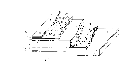
Re~erring now to Fig. 4, an alternative embodiment
40 o~ the present invention is illustrated. Multiple
switching device 40 includes a cover layer 41, a
piezoresistive layer 42, a base 46, and an activation region
47 which is a void. The shape o~ activation region 47 is
de~ined by a series o~ layered spacer elements 45a, 45b,
45c, 45d, and conductive layers 43 and 44a, 44b, 44c, and
44d.
More particularly, cover sheet 41 is a ~lexible
non-conductive sheet pre~erably ~abricated ~rom an
elastomeric synthetic polymer. The piezoresistive material
42 is pre~erably a piezoresistive cellular ~oam such as
described above, and is positioned above the top conductive
layer 43 with which the piezoresistive layer 42 is in
electrical contact. The conductive layers 43, 44a, 44b,
44c, and 44d can be, ~or example, metallic ~oils adhesively
bonded to the respective spacer elements directly below, or
may be conductive coatings deposited thereon. The spacer
elements 45a, 45b, 45c, and 45d are insulative layers o~
predetermined thicknesses, or heights. As shown in Fig. 4,
the spacer elements have similar heights. However, they can
also be ~abricated with di~erent heights. The heights
determine the amount of pressure or ~orce applied to the top
o~ the multiple switching device 40 necessary to activate
the next level o~ circuitry. Base 46 can be rigid or
-30-
CA 02219092 1997-10-24
W 096/34403 PCTrUS96/0~67
~lexible and can be a tough non-conductive material as
described above.
The activation region 47 is funnel shaped with
stepped sides. As seen from the top it is preferably
circular although angled shapes such as triangles, will also
work. As can be seen from Fig. 4, the diameter of the
opening 47a in the upper most spacer element 45a is greater
than the diameter of opening 47b in spacer element 45b, each
successively lower spacer element having an opening diameter
less than the one above. The top conductive layer 43 is
connected to a power source P and is designated as the
"emitter" electrode. The remaining conductive layers 44a,,
44b, 44c, and 44d are designated as the "receiver
electrodes" and may individually be connected to di~erent
respective circuits Zl~ Z2 ' Z3 ' Z4 '
Referring now to Fig. 5, when the multiple
switching device 40 is actuated by a ~orce F pressing down
on the cover sheet 41, the piezoresistive ~oam 42 is pressed
down into the activation region 47, and makes electrical
contact with one or more o~ the remaining conductive layers
44a, 44b, 44c, and 44d depending on the magnitude of ~orce
F. As each contact is successively made, a new circuit is
actuated. Thus, ~or example, circuit Z1 can be used to
accomplish one function, circuit Z2 can be dedicated to
another purpose or other machinery, and so on for Z3, and
Z4. Conductive layer 43 serves as the common emitter
-31-
CA 02219092 1997-10-24
W 096/34403 PCTrUS96/0~67~
electrode providing the power ~or receiver electrodes 44a,
44b, 44c, and 44d.
While ~our spacer elements are shown in multiple
switching device 40, it should be recognized that any number
of spacer elements may be used, and the heights o~ the
spacer elements may be varied in accordance with the
application for which the device 40 is used.
Re~erring to Fig. 6, an embodiment o~ the
invention is shown which can detect a shear ~orce, i.e., a
~orce which is parallel to the plane de~ined by the planar
top sur~ace of the switching device. A ~orce directed
vertically downward onto the cover sheet in a direction
normal to the plane de~ined by the top sur~ace o~ the
switching device has no shear component. However, i~ the
downward ~orce is at an angle ~rom the vertical orientation
it will have a vector component which is parallel to the
plane o~ the top sur~ace, this vector component constituting
a shear ~orce or stress.
As seen in Fig. 6, switching device 60 includes an
insulative cover sheet 61 with a conductive ~ilm or coating
62 on the underside thereo~. The conductive ~ilm 62 serves
as an emitter electrode. The cover sheet 61 and conductive
~ilm 62 are pre~erably elastomeric. Piezoresistive ~oam
layer 63 is beneath the conductive ~ilm 62 and is in
electrical contact therewith Spacer element 64 is an
insulative layer o~ cellular polymer and is resiliently
CA 02219092 1997-10-24
WO 96134403 PCTIUS96105675
de~ormable. Spacer element 64 has an aperture 68 de~ining a
void space into which piezoresistlve ~oam 63 can enter upon
the application of a downward force to the cover sheet 61.
Primary receiver electrode 65 is aligned with aperture 68
such that when the piezoresistive foam 63 is moved into
aperture 68, contact is made between the piezoresistive foam
63 and primary receiver electrode 65 thereby closing the
electric circuit and initiating the switching action as
current flows between electrodes 62 and 65.
In addition to the primary receiver electrode 65,
the shear detecting switch 60 includes at least one and
pre~erably four or more secondary receiver electrodes 66a
and 66b positioned around and laterally spaced apart ~rom
the primary receiver electrode 65, and covered by spacer
element 64. Secondary receiver electrodes 66a and 66b can
be connected to di~erent electrical circuits.
Base 67 provides support ~or the device, the
primary receiver electrode 65 and the secondary receiver
electrodes 66a and 66b being mounted thereto. Base 67 can
be ~abricated from materials as mentioned above.
Referring additionally now to Figs. 7 and 8, it
can be seen that when a ~orce F is directed vertically
downward on the cover sheet without any lateral vector
component (i.e. without any shear stress) as shown in Fig.
7, the piezoresistive ~oam layer 63 ~ills aperture 68 and
makes contact with the primary receiver electrode 65, but
CA 02219092 1997-10-24
W O 96/34403 - PCTrUS96/05675
not the secondary receiver electrodes 66a or 66b. In Fig.
8, force F is shown having a shear component, i.e., force F
is at an angle to the vertical orientation. As shown in
Fig. 8, secondary receiver electrode 66a is on the side of
the primary receiver electrode 65 in which the shear force
is directed. Spacer element 64 is thereby moved to uncover
secondary receiver electrode 66a, with which the
piezoresistive foam makes electrical contact in addition to
primary receiver electrode 65. Secondary receiver electrode
66b on side of the primarily receiver electrode 65 opposite
to the direction of applied shear, remains covered and is
not activated. Thus, the direction in which shear ~orce is
applied can be detected. Additionally, the magnitude o~ the
vector components o~ force F can also be measured since the
resistance o~ the piezoresistive foam will vary in
accordance with the applied compressive force, as discussed
above with respect to the aforementioned mat switching
devices. When the shear force is removed, the spacer
element resiliently returns to its initial configuration.
Re~erring now to Figs. 9 and 10, another shear
detecting switching device 70 is shown. Switching device 70
includes an insulative base 79 with a patterned array of
primary receiver electrodes 77 positioned in alignment with
apertures 78 of a rigid insulative spacer element 76. A
primary piezoresistive foam layer 75 is positioned above the
spacer element 76 such that in the initial uncompressed
-34-
CA 02219092 1997-10-24
W 096/34403 PCTtUS96tO567~
configuration of the device 70, a gap exists between primary
piezoresistive foam layer 75 and the primary receiver
electrodes 77. Above the primary piezoresistive foam layer
75 is an elastomeric insulator sheet 73 having top and
bottom conductive coatings 74b and 74c, respectively. The
conductive coatings, or films, 74b and 74c serve as emitter
electrodes and may be electrically connected to each other
or to parts of different electrical circuits. A secondary
layer 72 of piezoresistive foam is stacked above top
conductive layer 74b and is in electrical contact therewith.
The secondary piezoresistive foam layer 72 has a plurality
of conical peaks 72a which project upward. Alternatively,
72a can be a conductive elastomer.
Insulative cover sheet 71 is positioned above the
secondary piezoresistive foam layer 72 and has a plurality
of apertures 71a through which conical peaks 72a are
disposed such that the piezoresistive foam peaks 72a project
above the top surface of the cover sheet 71. At least one,
and preferably several, secondary electrodes 74a are
disposed around each aperture 71a of the cover sheet 71 on
the top surface thereof.
Referring now to Fig. 10, a downward force F with
a shear component is applied to switching device 70. The
primary piezoresistive layer 75 is moved through apertures
78 into contact with primary receiver electrodes 77. Also,
the conical peaks 72a bend over in the direction of the
CA 02219092 1997-10-24
W 096/34403 PCT/US96/0~67
shear ~orce to make electrical contact with secondary
receiver electrodes 74a thereby completing the electrical
circuit path between top emitter electrode 74b and secondary
receiver electrodes 74a. The direction and magnitude o~
both the shear can be measured by determining which o~ the
secondary receiver electrodes 74a are activated and the
amount o~ current ~lowing ~rom the top emitter electrode 74b
thereto. Likewise, the magnitude o~ the downward vector o~
the force can be determined from the current ~lowing from
bottom emitter electrode 74c to primary receiver electrodes
77. Moreover, the lateral position o~ the force F on the
top surface of the device 70 can be indicated by determining
which o~ the primary receiver electrodes 79 are activated.
Thus, a detailed measurement o~ position, magnitude and
direction of an applied ~orce can be made. The resolution
o~ the measurement depends upon the number, size, and
placement o~ receiver electrodes.
Corresponding mat switch 35 has tabs 36 configured
and dimensioned to engage slots 32, and slot areas 37 ~or
receiving tabs 31 of safety mat 30.
The tabs and corresponding slots provide mats 30
and 35 with the ability to interlock. Once engaged mat
switches 30 and 35 are resistant to separation by a lateral
~orce. It can readily be appreciated that tabs can be
incorporated on more than one edge of the mat switch and
that many mats can be interlocked to ~orm a single
CA 02219092 1997-10-24
W 096/34403 PCTrUS96/05675
contiguous structure. The mats may be connected
electrically, as well as physically, in series or parallel
circuits.
The mat switch construction of the present
connection permits the active surface area of the mat to
extend even into the tabs 31, 36. Thus, the tabbed area
does not represent a dead zone.
Referring now to Fig 17, a circuit 50 is shown in
which any o~ the mat switches of the present invention may
be employed to operate a relay.
Circuit 50 is powered by a direct current source,
i.e., battery 51, which provides a d.c. voltage VO ranging
from about 12 to 48 volts, preferably 24 to 36 volts. The
safety mat A can be any of the embodiments of the invention
described above.
Potentiometer Rl can range from 1,000 ohms to
about 10,000 ohms and provides a calibration resistance.
Resistor R2 has a fixed resistance of from about 1,OOo
ohms to about 10,000 ohms. Transistors Ql and Qz provide
amplification of the signal from the safety mat A in order
to operate relay K. Relay K is used to close or open the
electrical circuit on which the machinery M to be controlled
operates. Capacitor Cl ranges from between about 0.01
microfarads and 0.1 micro~arads and is provided to suppress
noise. K can be replaced with a metering device to measure
force at A. This would require adjusting the ratio of Rl
CA 02219092 1997-10-24
W 096/34403 PCTIUS96/0~67~
and A (compression vs ~orce) to bias transistors Q1 and Q2
into their linear amplifying range. This circuit represents
an example of how the mat may be activated. Many other
circuits including the use of triacs can be employed.
The various electrodes of the mats switches 40,
60, and 70 may be incorporated into separate electrical
circuits of the type shown in Fig. 17. Activation of the
relay corresponding to a particular circuit would then
indicate that longitudinal pressure or shear force of a
certain magnitude or in a certain position on the mat has
occurred. The multiple outputs o~ the relays may be the
input of a preprogrammed guidance control, or other control
or response means.
The present invention can be used in many
applications other than safety mats for machinery. For
example, the invention may be used ~or intrusion detection,
cargo shi~t detection, crash dummies, athletic targets (e.g.
baseball, karate, boxing, etc.), sensor devices on human
limbs to provide computer intelligence for prosthesis
control, feedback devices for virtual reality displays,
mattress covers to monitor heart beat (especially for use in
hospitals or ~or signalling stoppage of the heart from
sudden infant death syndrome), toys, assisting devices for
the blind, computer input devices, ship mooring aids,
keyboards, analog button switches,"smart" gaskets, weighing
scales, and the like.
-38-
CA 02219092 1997-10-24
W 096134403 PCTrUS96/05675
It will be understood that various modi~ications
may be made to the embodiments disclosed herein. Therefore,
the above description should not be construed as limiting,
but merely as exemplifications of preferred embodiments.
Those skilled in art will envision other modifications
within the scope and spirit of the claims appended hereto.