Note: Descriptions are shown in the official language in which they were submitted.
CA 02219389 1997-10-27
ty
METHOD AND APPARATUS FOR OPTICAL SIGNAL PROCESSING BY
PHOTO-INDUCED LOSS AND/OR GAIN GRATINGS
The present invention relates to optical signal
processing. More part1C111ar1y, the present invention
relates to the use of multiple-beam optical interference
to induce a loss or gain grating in a saturable medium,
and the application of this induced grating to provide
optical signal processing functions to a lightwave
communication signal.
3A K RO TND O THR TNVRNT'LON
In all forms of lightwave communications systems,
noise from a variety of causes can interfere with the
users' communications. Examples of corrupting noise
include noise originating as part of the transmitted
signal, noise created in the process of digital encoding
and signal formatting, noise introduced by crosstalk in
~pi~pl arc ~r refl a~ti~n~ ~r ~p tWai vvtWpoileiltS~ itoiSe
caused by the distortion of the signal or creation of
unwanted harmonic products due to nonlinearities at the
transmitter or receiver, quantum or modal noise within
the optical source, and so forth.
The presence of noise in lightwave communications
systems is annoying or distracting to users, can
adversely affect speech quality, can reduce the
CA 02219389 1997-10-27
2
' performance of speech coding and speech recognition
apparatus, and in some instances completely render the
optical information signal unintelligible to the system
and thus the user. As a consequence, there exists a
need to filter such noise: from an optical information
signal.
Lightwave communications systems involving optical
amplifiers have a particular problem with amplified
spontaneous emission (ASE) noise. ASE noise arises in
the amplification process>. The resonant medium that
provides amplification by the process of stimulated
emission also generates spontaneous emission. The light
arising from spontaneous emission is independent of the
input to the amplifier, and represents a fundamental
source of amplifier noise. Whereas the amplified signal
has a specific frequency, direction, and polarization,
the ASE noise is broadband, multidirectional, and
unpolarized. As a consequence it is possible to filter
out some of this noise by following the amplifier with a
narrow bandpass optical f=filter.
Fixed optical filters such as multilayer dielectric
coatings can be used to filter out ASE noise.
Properties of such fixed optical filters are discussed,
for example, in a book edited by Walter G. Driscoll and
William Vaughn, titled Handboo_k_of o i ~, Chapter 8,
Mcgraw-Hill, New York, 1978.
There are many prob~'_ems, however, associated with
the use of fixed optical filters. For example, fixed
optical filters require precise wavelength matching of
the filter and the lightwave signal. This requirement
increases the cost of the' filter and the entire system.
Furthermore, light sources are susceptible to aging,
leading to a mismatch of the lightwave signal to the
fixed filter over time, and necessitating repair or
replacement. Fixed filters are also sensitive to
environmental changes. Consequently, the environmental
conditions surrounding the filter must be carefully
CA 02219389 1997-10-27
s
. 3
controlled and monitored. Environmental changes such as
temperature fluctuations can distort the filter
wavelength thus requiring repair or replacement. I:n
addition, if the lightwave communications system is
upgraded and uses a different or additional wavelength
for the transmission signal, the filter must be rep:Laced
to match the new wavelength. For those systems using
multi-wavelength signals, a filter is required for Each
wavelength, greatly increasing the initial and
replacement costs associated with each filter.
Another type of filter capable of filtering out. ASE
noise is a refractive-index filter. Examples of
refractive-index filters are discussed in " Transient
Bragg reflection gratings in erbium-doped fiber
amplifiers," by S. J. Frisken, Ont~c~~ r,PrtAr~, Vol. 17,
No. 24, December 15, 1992, and "Nonlinear wave mixing
and induced gratings in erbium-doped fiber amplifiers,"
by Baruch Fischer, o ~ ~ r, t Pr , Vol . 18 , No . 24 ,,
December 15, 1993.
Tunable refractive-index filters such as those
discussed 1n Fr~~ and F~induce a refractive-
index grating in a doped medium to reflect an optical
information signal to an output port while unwanted
noise is passed through the filter to be absorbed
elsewhere. Refractive-index filters split a control
wave using an optical coupler. These filters then
direct a beam through each end of a doped medium, such
as erbium doped (Er-doped) fiber. Propagating the beams
in opposite directions creates a standing wave, which in
turn induces a refractive-index grating capable of
reflecting certain wavelengths of light. By careful~_y
controlling the refractive-index grating, the
wavelengths representing noise can be separated or
"filtered" from the signal wave.
These filters, however, are problematic. The
refractive-index grating merely re-routes the unwanted
noise without absorbing it, so care must be taken to
CA 02219389 1997-10-27
4
° avoid leakage of the noise back into the communical=ion
system. In addition, these filters require the use of
both a pump light source to produce the gain in the Er-
doped fiber, and a tuning-control light source to create
the standing wave. This increases the number of
required components for filters of this type and greatly
increases their cost. Further, the wavelength of t:he
tuning-control source must be precisely matched to that
of the signal, requiring a wavelength-locking feedk~ack
loop control, adding even greater complexity. Fin~~lly,
adding a new signal wavelength to increase capacit~~
would require addition of another tuning control source
in every filter, making such upgrades prohibitivel~~
costly.
Moreover, refractive-index filters split the wave
from the tuning-control light source and direct each
beam through both ends of the doped medium to induce the
refractive-index grating. This necessitates additional
optical components such--as couplers, loops and
polarization controllers. These extra components n.ot
only increase the cost of the filter, but also create
instability of the stand_Lng wave because of the error
introduced to the beams as they pass through these
additional components. Since loss of coherence between
the two beams will destroy the signal output, this
instability severely limits the robustness of the
system.
In addition to noise., power control is a critical
issue in lightwave communications systems. Systems
using multiple wavelength channels can suffer severe
penalties if the channel power levels vary too widely.
Slight wavelength dependE:nce of the optical amplifier
gain can lead to such imf>alances after an amplifier
chain., Therefore, automatic adjustment of channel
levels, known as channel equalization, must be performed
periodically.
One method of channel equalization is to separ<~te
CA 02219389 1997-10-27
the wavelengths, measure t:he power of each one, and
adjust the gain or loss e~cperienced by each channel
before recombining them. Equipment to perform this
channel-by-channel adjustment, however, is expensive and
can degrade the signal-to--noise ratio of the channels.
A twincore erbium doped fiber amplifier (TC-EDF.A)
with a channel equalization of 1 decibel (dB) is
discussed in a conference report titled " Channel po~Ner
equalizing WDM link incorporating twincore erbium doped
fibre amplifiers " by Oliver Graydon et al_, Summaries
of the papers presented at. the topical meeting optical
A~n'i ; f; Pry nd Th ; r Ap~i ; one, Monterey, California,
July 11-13, 1996. When multiple channels are launched
into one core of a pumped Er-doped twincore fiber, the
channel powers couple from core to core along the length
of the fiber. This beatlength, however, is wavelength
dependent and thus the ch<~.nnels become periodically
spatially separated. Thi:a decoupling of the channels
gives the Er-doped fiber amplifier inhomogeneous
saturation characteristics and allows the channels to
saturate the gain to some degree independently. As a
result weaker channels will receive more gain than
stronger channels. This intrinsic equalizing effect
keeps the channels propagating with constant powers
along the TC-EDFA cascade.
A problem with the .~r_aydon equalizer is that it
requires the use of dual-core fiber. Dual-core fiber
requires precisely contro:Lled coupling, making the
Gra~rdon equalizer difficu_Lt to manufacture. Further, it
is difficult to eliminate the undesired polarization and
wavelength dependence requirements.
Accordingly, it becomes readily apparent there
exists a need for a method and apparatus for
implementing a self-tunin<~ filter and a self-adjusting
channel equalizer that is robust and solves the above-
discussed problems.
1
CA 02219389 1997-10-27
- S TMMARY p THF T1'~TFT'TTrnr~
6
The present invention relates to a method and
apparatus for creating an interference induced grating
in a saturable medium, and the application of this
induced grating to provide optical signal processing
functions to a lightwave: communications signal. T~No
embodiments of the present invention provide self-~~uning
noise filtering and self-adjusting channel equaliz<~tion
of lightwave communications signals which are valu<~ble
in constructing robust, flexible, and less expensi~re
communications systems.
The automatic noise filtering and channel
equalization of lightwave communications signals is
accomplished by inducing loss or gain gratings,
respectively, in a saturable absorption medium. Tree
apparatus discussed in detail below incorporates the
saturable medium into a single-mode guided wave
structure which has a reflector at one end, and an
input/output port at the other end. Light entering the
input/output port interferes with light reflected off
the reflector to create a standing wave pattern of
intensity maxima and minima. This intensity standing
wave induces a saturation grating in the saturable
medium to provide the de:~ired effects.
With respect to the noise filtering embodiment of
the invention, a loss gr<~ting is created having areas of
low and high absorption <~.long the length of the wave
guide medium. These areas of low and high absorption
substantially coincide with the intensity maxima anal
minima, respectively, of the signal wave. Therefore,
the signal energy is concentrated in low absorption
areas, and the signal wave loses little energy as iv
passes along the doped medium. Noise waves, however,
operate at different wavelengths from the signal wa~Te.
Thus, it is extremely likely that some noise wave peaks
will occur at regions of high absorption along the
1
CA 02219389 1997-10-27
7
length of the medium, thereby attenuating the noise.
The channel equalization embodiment can be
constructed using the same apparatus described for the
noise filter, with the addition of a source of pump
light and a means for introducing the pump light into
the saturable medium. The wavelength of the pump light
is outside the signal band, and is chosen to provide
gain in the medium. As before, a standing wave is
generated by the signal light, inducing a gain grating
with reduced gain at the intensity maxima. The degree
of gain reduction, or saturation, depends on the
intensity level, leading to a desirable automatic gain
control (AGC) effect.
The present invention provides significant
advantages over optical :signal processing devices
currently used for optical filtering and channel
equalization. First, the. present invention provides
self-tuning filters and self-adjusting channel
equalizers, where previous filters and channel
equalizers needed external tuning control. Second,
because signals enter and exit the doped medium by 'the
same port, the present invention requires fewer optical
components. This decrea~>es system costs as well as the
introduction of noise or error in the signal. Thir<3,
the present invention is not as sensitive to
environmental conditions as previous filters and channel
. equalizers. Fourth, the present invention allows system
upgrades without the need. to replace the optical fi7_ters
and channel equalizers (and associated optical
components). Fifth, the compact reflector-based
structure for generating the standing wave reduces
instability and improves robustness. Sixth, the preaent
invention is inherently polarization-independent.
Seventh, the present invention can use single-core fiber
or planar waveguide which are easier to manufacture than
twin-core fiber. Finally, the filter embodiment of the
present invention does not require the addition of pump
CA 02219389 2000-10-20
8
light into the doped medium, and therefore requires fewer
optical components. These and other advantages of the
present invention solve many problems associated with
previous optical signal processing devices.
In accordance with one aspect of the present
invention there is provided an apparatus for optical
signal processing, comprising: a single-mode guided wave
structure including a saturable medium, said structure
having a first and second end; a reflector at said first
end of said structure; and an input/output port at said
second end of said structure such that light entering said
input/output port interferes with light reflected off said
reflector to create an induced interference grating.
In accordance with another aspect of the present
invention there is provided a method for filtering noise
from an optical signal made up of at least one discrete
wavelength of light, comprising the steps of: introducing
an incoming optical signal into one end of a single-mode
guided wave structure having a saturable absorber; and
reflecting said incoming optical signal wave back onto
itself to create a standing wave with local intensity
maxima, wherein said standing wave induces a loss grating
with areas of low absorption coincident with said
intensity maxima.
With these and other objects, advantages and features
of the invention that will become hereinafter apparent,
the nature of the invention may be more clearly understood
by reference to the following detailed description of the
invention, the appended claims and to the several drawings
attached herein.
BRIEF DESCRIPTION OF THE DRAWINGS
FIG. 1 is a block diagram of a system in which an
embodiment of the present invention may be deployed.
CA 02219389 2000-10-20
8a
FIG. 2.A is an absorption versus wavelength plotting
for a saturable absorber used in accordance with an
embodiment of the present invention.
FIG. 2.B is an absorption versus wavelength plotting
for spectral hole-burning of a saturable absorber used in
accordance with an embodiment of the present invention.
FIG. 2.C is an absorption versus wavelength plotting
of a spectral hole typical of common saturable absorbers.
FIG. 3 is a block diagram in accordance with an
embodiment of the present invention.
FIG. 4 is a light intensity versus position plotting
of an optical information signal and noise wave as an
example of the type of signal processed in accordance with
an embodiment of the present invention.
FIG. 5 is an absorption versus position along the
waveguide plotting showing an example of the type of loss
grating created in accordance with an embodiment of the
present invention.
FIG. 6 is a block diagram in accordance with an
embodiment of the present invention.
CA 02219389 1997-10-27
9
FIG. 7 is a block diagram in accordance with an
embodiment of the present invention.
FIG. 8 is a light intensity versus position
plotting when a multiwavelength optical signal
comprising two unequal channels is present in accordance
with an embodiment of the present invention.
FIG. 9 is a gain versus position plotting showing
the creation of a gain grating according to an
embodiment of the present invention.
The invention will :be described in connection with
a lightwave communications system. The invention is
essentially an optical signal processing device and
method for creating a gain or loss grating in a single-
mode guided wave structure having a saturable medium.
Two possible embodiments of this device include an
optical filter and channel equalizer. The invention
enhances the quality of a received optical information
signal and controls the ~gower levels of multiple
communications channels.
Referring now in detail to the drawings wherein
like parts are designated by like reference numerals
throughout, there is illustrated in FIG. 1 a block
diagram of a system in which an embodiment of the
present invention may be deployed.
FIG. 1 illustrates an exemplary lightwave
communications system, constituting signal transmitted
entering optical communications transmitter 12.
Transmitter 12 has optic<~l source driver 13 that
converts signal 10 to a drive current that intensity
modulates the source. Optical source driver 13
generates the energy that= is coupled into transmission
medium 19, which is typically optical fiber. The energy
propagates down transmis:~ion medium 19 and is attenuated
to a degree. To compensate for this attenuation, the
CA 02219389 1997-10-27
energy is put into optical amplifier 14 which incre=ases
the amplitude of an optical field while maintainin<~ its
phase. A byproduct of optical amplification of the
energy is the introduction of ASE noise.
To reduce this ASE noise the energy is passed
through optical device 15. Optical device 15 may also
automatically adjust the gain for each wavelength of a
multi-wavelength channel. Although optical device 15 is
shown immediately after optical amplifier 14, optical
device 15 can be placed in receiver 17, or anywhere: in
the system where filtering or channel equalization is
desired.
After passing through optical device 15, the e=nergy
is placed back on transmission medium 19. The enex-gy
exits transmission medium 19 at the other end and is
coupled into photodetect~or 16. The light energy that is
absorbed in photodetector 16 is converted to a
photocurrent. This photocurrent is then amplified in
receiver 17 and converted to the proper signal format
for signal received 18 at the output.
One embodiment of the present invention comprises a
self-tuning optical filt<~r based on spatial hole-burning
in a saturable optical medium. One example of a
saturable optical medium is Er-doped fiber. Optical
filters are important in amplified systems, including
soliton-based systems, to control the ASE noise which
arises in the amplificat_i.on process. Since the filter
wavelength must closely match the signal wavelength,
both signal source and filter must be rigidly controlled
and stabilized when fixed filters are used. Much more
flexible operation could be achieved if the filter were
self-tuning, ~, able t_o follow the signal wavelength.
Such a self-tuning filter could be realized by
passing the signal light through a saturable absorber,
CA 02219389 1997-10-27
11
if the absorption of different wavelengths were
independent. The suppression of absorption at a
particular wavelength is called spectral hole-burn_ng.
FIG. 2.A is an absorption versus wavelength
plotting for a saturable absorber used in accordance
with an embodiment of the present invention. FIG. 2.A
depicts a saturable absorber with no signal or weal':
signal. As can be seen by the graph, absorption i:> high
under these circumstances.
FIG. 2.B is an absorption versus wavelength
plotting for spectral hole-burning of a saturable
absorber used in accordance with an embodiment of t:he
present invention. When a strong signal is passed
through a saturable absorber, it creates an area of: low-
absorption near the signal wavelength, as shown in FIG.
2.B.
FIG. 2.C is an absorption versus wavelength
plotting of a spectral hole typical of common saturable
absorbers. As shown in :fIG. 2.C, the spectral hole: in
common saturable absorbers is too broad in wavelength to
be of practical use.
Accordingly, the present invention uses spatial
hole burning, which suppresses absorption at certain
locations in the absorber, rather than spectral hole-
burning. The wavelength filtering effect is achieved by
routing or concentrating different wavelengths of light
to different locations in the absorber.
One embodiment of the present invention uses a
single-mode guided-wave structure, an example of which
is a single-core, Er-doped fiber, with an end reflector
to create a standing wave=_ of intensity maxima in the
fiber. The standing waves is created by passing an
optical signal through a counter-propagating replica of
the signal within the single-mode guided-wave structure.
The counter-propagating replica of said signal is
created using the end reflector to reflect the incoming
optical signal back towards itself.
' CA 02219389 1997-10-27
12
The Er-doped fiber is unpumped (or possibly
underpumped) so that it produces loss rather than gain.
The loss in this fiber, however, can be suppressed by
saturating it with a strong signal. In the two-pa:~s
reflection geometry, the strong signal magnitude
suppresses absorption Qrily at fixed locations. The:
locations are separated by distance of (n) times (w)
divided by two, where (n) is the refractive index and
(w) is the signal wavelength.
Since the signal wave is concentrated at
substantially the areas of low absorption, the signal
suffers only slight absorption. Noise at another
wavelength will be concentrated at a different set of
locations, some of which will be areas of high
absorption. Thus, the broadband noise will be
attenuated much more strongly than the signal, achieving
the desired self-tuning filtering effect.
The present invention can also use saturable
absorbers other than Er-doped fiber. In particular, the
present invention can also use optical waveguides
fabricated on planar substrates, such as glass, lithium
niobate, or semiconductor substrates. Moreover, tr.e
optical waves need not necessarily be guided. For
example, back-reflection of plane waves will produce a
similar pattern of wavelength dependent intensity
maxima.
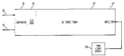
FIG. 3 is a block diagram in accordance with an
embodiment of the present= invention. Input signal wave
28 is directed into input/output (I/O) port 20 by
separator 26. Practical examples of separator 26
include a circulator or :3 dB directional coupler. I/O
port 20 transfers input :signal wave 28 into a saturable
absorber. This embodiment of the present invention uses
Er-doped fiber 22. Input= signal wave 28 propagates
along Er-doped fiber 22 until reaching reflector 24.
Practical examples of reflector 24 include a metallic
mirror or dichroic coating. Reflector 24 reflects input
CA 02219389 1997-10-27
13
signal wave 28 creating output signal wave 30. Oui~put
signal wave 30 propagates away from reflector 24 and
runs directly through input signal wave 28. Output=
signal wave 30 exits the Er-doped fiber through I/O port
20 by separator 26.
When two or more optical waves are present
simultaneously in the same region of space, an
interference pattern is produced, and the total
wavefunction becomes the sum of the individual
wavefunctions. This sum of individual wavefunctions
forms a waveform referred to as a standing wave. '.'he
standing wave caused by input signal wave 28 and output
signal wave 30 saturates the absorption of Er-doped
fiber 22, creating a periodic array of high-absorption
and low-absorption regions along the length of Er-doped
fiber 22, which is referred to herein as an interference
induced grating. The low-absorption regions
substantially coincide with intensity maxima 32 (shown
in FIG. 4) of input signal wave 28, so there is
relatively little attenuation of output signal wave: 30
as it exits I/O port 20 by separator 26.
FIG. 4 is a light intensity versus position
plotting of an optical information signal and noise: wave
as an example of the type of signal processed in
accordance with an embodiment of the present invention.
The position of the optical information signal and
noise wave is measured in terms of wavelengths (~0) from
the reflector which is represented by the right axis,
with the axis points labeled as X0/4, 30/4 and 50/4.
FIG. 5 is an absorpi=ion versus position along the
waveguide plotting showing an example of the type cf
loss grating created in <~ccordance with an embodiment of
the present invention.
Together, FIG. 4 and FIG. 5 provide a more complete
picture of the optical s_Lgnal processing of an
embodiment of the present. invention. As displayed in
FIGS. 4 and 5, intensity maxima 32 substantially
CA 02219389 1997-10-27
14
coincides with low-absorption area 44 of the loss
grating. Similarly, intensity minima 34 precisely
coincides with high-absorption area 42 of the loss
grating. As input signal wave 28 passes along the
length of Er-doped fiber 22, intensity maxima 32 of
input signal wave 28 pas:~es through low-absorption area
44 while intensity minima 34 of input signal wave 28
passes through high-absorption area 42 of the loss
grating. Therefore, the energy of output signal wave 30
is relatively undiminished as it passes along the length
of fiber 22 to I/O port :?0.
Noise wave 40, however, comprises a different
wavelength than input signal wave 28. Therefore, the
intensity maxima 38 of noise wave 40 will invariably
pass through high-absorption area 42, thereby
attenuating the energy of noise wave 40. The amount of
noise reduction is discussed in the appendix attached
hereto, which comprises a quantitative theory of the
present noise filter, with numerical results for some
cases of interest.
AITTOMATT p,ND TN FND N'1' AD TT TN T HANK .T, RQ 1AT,T9,ATTON
RMBO TM .NT
FIG. 6 is a block diagram in accordance with
another embodiment of the: present invention for
automatically and independently adjusting channel
equalization. Such channel equalization can be achieved
in a fiber-reflector pair similar to that shown in fIG.
3, with the addition of ~>umping light from light source
29 into Er-doped fiber 22 to produce gain in Er-doped
fiber 22. The pump light is introduced into Er-doped
fiber 22 through end reflector 24, which can be made of
dichroic coating. End rE:flector 24 made of dichroi~~
coating passes the pump wavelength band but reflect; the
signal wavelength band. Alternatively, the pump li<~ht
can be introduced into Er-doped fiber through I/O port
20.
CA 02219389 1997-10-27
As with the previou:a embodiment discussed in
reference to FIG. 3, a si~anding wave is generated,
inducing a gain grating with gain saturation at the.
intensity maxima of inpui~ signal wave 28. The degree of
gain saturation depends on the field intensity, leading
to a desirable AGC effect:. Because each wavelength.
channel has its own set of locations for intensity
maxima, there is an independent AGC effect for each.
channel, leading to the desired equalization.
FIG. 7 is a block diagram in accordance with
another embodiment of thE: present invention. The
embodiment shown in FIG. 7 is similar to that shown in
FIG. 6, but inserts wavelength division multiplexes
(WDM) 27 between separator 26 and input/output port 20
to introduce pump light into the saturable absorber.
Alternatively, WDM 27 can be placed before separator 26.
FIG. 8 is a light intensity versus position
plotting when a multiwavelength optical signal
comprising two unequal channels is present in accordance
with a channel equalization embodiment of the present
invention. The plotting shows a stronger channel 46 of
wavelength ~0 and a weaker channel 56 of wavelength ~1.
The position of stronger channel 46 and weaker channel
56 is measured in terms of wavelengths (~0) from the
reflector which is represented by the right axis, with
the axis points labeled as X0/4, 30/4 and 50/4.
FIG. 9 is a gain versus position plotting showing
the creation of a gain grating according to a channel
equalization embodiment of the present invention.
Together, FIGS. 8 and 9 illustrate the mechanism of
automatic, multichannel gain equalization in an
embodiment of the present invention. The intensity
maxima 32 of the standing wave associated with the
stronger channel 46 are high enough to cause saturation
of the gain medium, resulting in the creation of gain
grating 54. The gain minima 48 substantially coincide
with the intensity maxima 32, assuring that the stronger
CA 02219389 1997-10-27
16
channel 46 will experience reduced gain, compared to the
unsaturated gain 50. The intensity maxima 52 of the
standing wave associated with the weaker channel 56 are
not strong enough to cause significant gain saturation,
and they do not generally coincide with gain minima 48.
Therefore, over many periods of the gain grating, the
weaker channel 56 will experience higher gain than the
stronger channel 46, and partial gain equalization is
accomplished. In a complete communication system, this
partial equalization may~ be repeated over many sta~~es to
achieve the desired degree of gain equalization.
Although several embodiments are specifically
illustrated and described herein, it will be appre<~iated
that modifications and variations of the present
invention are covered by the above teachings and within
the purview of the appended claims without departing
from the spirit and intended scope of the invention.
APPENDIX CA 02219 is9 1997-10-27
This Appendix describes the action of the self-tuning filter based on the
principle of induced loss
gratings in a saturable absorber. In brief. an optical signal is sent into a
length L of fiber containmci a
saturable absorber in the core, reflected back on itself ~o create a standng
wave, then output from the
same port at which it entered. If the standing wave is strong enough to
saturate the absorption, a oss
grating will be induced which will attenuate noise signals at other
wavelengths. The method presumes
that the spectral density at the signal wavelength is much stronger than the
spectral density at the noise
wavelengths. For simplicity, consider the case of a strong, single-frequency
pump wave and a weak.
single-frequency probe wave.
PART I -- INDUCED LOSS GRATING and PUMP ABSORPTION
The intensity of the pump wave and the toss profile in the fiber interact, and
so they must be compu~'ed
self-consistently. The UO port is assumed to be Located at x=L and the
reflector is assumed to be
located at x=0. Consider first the refteded wave. fts amplitude is:
AR(x)=A0. F(x).e~iw.~t- R~ + i~$~o
v
The constant Ap is the amplitude at x=0, the constant ø is the phase shift
associated with the refledon,
and the function F(x) describes the reduction in intensity or power when
propagating from location 01'0
location x. It should be noted for future use that this F(x) depends on the
spatial frequency and pha~~e
of the standing wave relative to the loss grating; it is not the same as the
loss experienced by a single
traveling wave. Assuming that the reflector is i 00% reflective, the incident
wave is then:
AI(x)gAO~F(x) z~ex~i~cu
v
Then the intensity at location x is made up of the inadent and reflected waves
I(x)=~IAI(z) + AR(x)I~2n
I(x) ~~~'I(x)~~Z+ ~~AR(x)~~2+ A~Z~ex~i~~2werV - ø~~ + Ao ~ex~y2wv
I(x)=A~ -~F(z) + F(x) + 2~cos~2~~-V - ~~,~o
Note that the intensity function is a cosine wave of CCN~tSTANT mapn~rde and
period xvl~
superimposed on a DC badcQround which increases ;gray from the rellectot. SMae
F(x) rt~t d6aeas~
morwtonicalty from its value of 1 at x~, we see that the modulation depth of
the ir~er~ity wave is ifJa96
at x~ and decreases from there.
In a saturabie absorber characterized by saturation intensity t~, the ~ten~y
sten~ng wave wilt ~err~erate
an absorption sranc~ng wave with the same sped frequency anci~heel~ ~po~dl--.
: .. :,.
a0
a(x)= o
(I + I(x)1
Is
At any point, the power absorption per unit length will be:
~(x)~I(x)~a(x)
Assuming that I(x) changes slowly, over many spatial periods, we can average
this loss over one period
to eliminate the periodic dependences.
v
x + m-
~av(x)$ ~ ~ a(x')~I(x') dx'
v~ n x
' CA 02219389 1997-10-27
18
_ ~-~ -u0 Fl t) ~ 1 dx~
AO-.~ I t I=( x~ + '_'.cos~Z.ca.x, _ ~~)
I + F( x ~
I
0
2w
a0 IO+ Il~cos(~)
Dav( x)~-.Is. d~,
2-rr Is+ IO+ II-cos(~)
0
where we have defined
2.tc. v' ~ IO AOz F x + F(x) II=?.AOz
( )
Continue to reduce integral
2~n
~ av( x )' -' I ~ I d
2a s ~ Is+IO+Il~cos(~),
0
Is II _
R IO+ Is r IO+ l:s
n
~av(x)s aO.Is. 2.a - 2~. I ~d~
2~n I + Y-cos( ~)
0
Obtain result from Table of Integrals, Spies, and Products, LS. Gradshteyn and
LM. Ryzhac, Academa;
Press, New York, 1965, sec. 2.553 It3.
a
I + 7~cos( ) d~ Z ~(t + y ~~(2~~ ~ 1 + ~ ,
r
0
I d?;= 'r (for 7 < i ; checked by numerical example)
I + y cos( ~ )
Then we have:
I
eav(x)~aOIs.~I
" CA 02219389 1997-10-27
I9
Substituting m for 13 and ;:. we find:
_ ~ I ~= i
~a~.~ sl=u0'Is~ I
I0t Is - II
~av( x)=aO.Is. I _ Is_
~IO(x) + ~Is ~ IIO~~IO(x) + CIs- II~
dav(:,)=aO~Is~ I - Is
2
A02 I + F(x) + Is - 4-A04
C ~(F(x) )
Aav(xW~O.Is. I _ I A0z
z K=-
~K~~ I + F(x)~ + I~ - 4-KZ Is
F( x )
The absorbed power will be drawn from the incident and reflected waves
according to their relative
intensities:
~I(x) I +II ~6av(x) ~R(x)-I RI Wav(x)
I R I R
O av( x ) F( x )z
~I(x)= z av( z
dR(.K) A x)~ I + F(x)
I + F( x )
But we also know, by the definition of F(x), that the loss from the reflected
wave between 0 and x is:
A~~(I- F(x))
so we have the integral equation which detemines F(x).
-x
A0z'(I-F(x))= ~R(x')dx'
0
This can be differentiated to yield the non-linear differential equation:
d F( x)=__ I Z.~R(x)a
dx AO
" CA 02219389 1997-10-27
' Try expanding in powers of K for a weak saturation result
j
._1Rr .W=u.~~ I~ I - I Fr tl- o
/ , ' ~ r 1 + Fr rl'~
(IUI I + F( x)J + 1~ - 4~K'
[~ 'F( t )
A (x)=a ~I_ F1x)~K I+F(x)~+Z~-F(x)' )~KZ+0(K3) o
R 0 '.~ ( I - F(x)Z)J
As K goes to 0, this becomes
~R(x)$a0.A02.F(x)a
Then the differential equation becomes
d F(x)=-aO~F(x)o
dx
which is clearly the correct result when there is no saturation of the
absorption. In the limit of large K
(strong saturation of absorption), the equation is:
d F(x)=-a0.ls~ F(x)2 0
dx A0z (1+F(x)Z)
An iterative solution can be achieved for arbitrary K. Taking K=5 as a
specific example
a 0 := 1 in m-t AO := 1 actually, a dummy variable
K:=5
eR(F) := a0. A0 I - 1 F'2
K ' ( l2 .(1+FZ)
~K~~F+F,+IJ -4~IC2
Npoints := 22 Nloops := 10 x'sd~ := 2
j := 0.. Npoints xj := x_step~ j + 0 TOL := 10 5
loop := 0.. Nloops
~- a 0''51 starting guess for F(x)
Ftv>j , o := exp 10 use lin interp of table for speed
FMS , (ooP + ( '= 2- I - 1 Z' ~ A R( tinterh( x, FMS (°°('~ , x'
) ) dx' + Flvi~ . (ooP
AO 0
,r ds\
dB( r ) := t 0~ log( r ) lin( dB ) := 10 ~ ~ l~
CA 02219389 1997-10-27
FLt, " FVt, . w",.;.. E ~~ . v!,~,~:~
! 1
dB~F~~.O~
dBCF?~~ ..i~
...... -10
dB~F~~ . 5
dB(FM . 6)
-15
20 ' -
0 10 20 30 40 5
x.
FMzo
FM
' CA 02219389 1997-10-27
LL
- PART II. ABSORPTION OF WEAK PROBE WAVE
The self-consistent calculaUon above gives the intensity of the pump beam and
the degree of local
absorption along the fiber. Thus the absorption of a weak probe beam can be
calculated. As noted
above, the power absorption per unit length at any point will be:
~ PR( '~ f - I PR( x >' at x )
As for the pump beam, the probe beam intensity has the form:
Ipr( x)=Apr~yFpr~ x) + Fpr( x) + 2~cos~.2~wpry - ~~~ n
For convenience, assume that the velocity and the reflector phase are the same
fcr the two waves. The
local absorption is periodic with the spatial period of the pump standing
wave, so rt can be expressexl as
a Fourier series, leading to:
Apr(x)=Ipr(x)'~Cm-cos~2-m~W-X~ + l~m~sin~2~m~c~-X
v/ v
m
making the usual assumptions about slow variation of all quantities relative
to the optical frequency, ii a
clear that the integral over macroscopic x will be non-zero only if
o~ prs mW
Since the useful wavelength band is much less than an octave, this will not
occur, and only the DC terms
will contribute significant absorption of the probe wave. Now
a0
a(x)~
1+K~~F+F+2-cos'2-c~~V-~~~
r
a( x)=
t + n-cos( ~,)
where
r= «o.F n= 2.K.F
F+K-(t+FZ) F+K-(t+F2)
Then the DC part of a(x) is:
2- n
C 0= r . 1 d~
2~n 1 + A-cos( i;)
0
C 0= r
1 - AZ
CO~aO. F
(F+K~(1+Fz))Z-4~KZ~F2
' CA 02219389 1997-10-27
23
- - Thus for the limit of small K
and for the i~m~t of large K
F
c0=a0'
Wl l - ~)
returning to the general form and restoring the slow x dependence, we find the
probe absorption per unit
length:
~pr(x)=Apr~y I + Fpr(x)~~a0._ F(x)
F r( x ) 2
p (F(x) + K~( 1 + F(x)2)) - 4~KZ.F(x)2
Considering now only the reflected wave
~pr_R(x)=~pr(x). Fpr(x)2 ~
I + F pr( x )
F Pr( x )2
Apr_R x)Wpr'
1 + F pr( x )
2 F( x )
~pr_R(x)=Apr .Fpr(x).a0.
(F(x)tK~((+F(x)2))Z-4~KZFx2
' ( )
Then normalize to the probe intensity to get an effective absorption
coeffiaent:
apr_eff(x)=a0' F(x)
2
(F(x)+K~(1+F(x)2)) -4~K2~F(x)2
For comparison, the equivalent quantity for the pump wave is:
a0 F F
ae~ K . ~. i _
1+ (K.(1+FZ)+F)2-4~F2.K2
Fnally, integrate over a to find the loss of the whole; filter in deabels:
-x
dBloss( x ) =10~ log exp - a pr eff{ x' ) d x''
0
-x
dBloss( x )=10~ log( exp( I ) ) ~ - a pr eff{ x ' ) dx'
0 ,
-x
dBloss( x ) _-10~ log( exp( 1 ) ) ~ a 0~ F( x' ) dx'
2
( F( x' ) + K~ ( i + F( x' )2 ) ) - 4~ Kz~ F( x' )2
0
CA 02219389 1997-10-27
Substitute in the tabular form of F(x) that was calculated above:
< w", ~~., >
h~t :: - :tt~t.r» v. F~1
dBtossJ :_ - 10~ log( erpl ( ) )~ ~ a0~ F~( Y~ ) d;K~
~F'( x' ) + K~( 1 + F'( x' )' ) )~ - ~i~K'~F'( x' )~
0
dBloss~ : _ -10- log( exp( 1 ) ) ~ ~ a 0 dx' a dB( exp( -1 ) ) _ x.3.43
0 a0 = 1
< Nlcbps>
ins_loss := 2~dB( FM )
<Ntoops> )
rejection := 2~( dB( FVi ) - dBloss
dBloss) x) ins_lossJ rejection
1
3
m := 0.. 4 LL := 6
12
18
y := 1 TOL := 10 g
Lm := root ( linterp( x , ins_loss , y ) + LLm , y)
a 0- Lm linterp~x , rejectioa , Lm)
1.467 1.727
4.397 4.604
8.975 7.096
2.10110 8.832
4.21610 9.246
Repeating the above calculation for various values of K, plots of noise
rejection and required fitter length
can be made as a function of normalized input power, with insertion loss as a
parameter.
CA 02219389 1997-10-27
LJ
Noise Reject ion of Self-Tuning Filter
12
8
c
_o
6
m
4
2
0
-10 -5 0 5 10 15 20
dB (Pin/Psat)
Normalized ~engt; h of Self-Tuning Filter
100
--f- hs. Loss = 1.0 dB
hs. Loss = 3.0 dB
-i- hs. Loss = 6.0 dB
--~E- hs. Loss = 12.0 dB
10 ---f-- hs. Loss = 18.0 dB- _ -------i-------
t
...
c
J 1
0.1 ~ ~ ~ ~ ~ . ~ ~ ~ ~ ~ ~ ~ ~ ~ ~ ~ ~ ~ ~ ~ ~~
-10 -5 0 5 10 15 20
dB (Pin/Psat)