Note: Descriptions are shown in the official language in which they were submitted.
CA 02220507 1997-11-07
WO 96/36145 PCT/US96/07741
-1-
DATA TRANSMISSION SYSTEM WITH A LOW PEAK-TO-AVERAGE POWER
RATIO BASED ON DISTORTING FREQUENTLY OCCURRING SIGNALS
BACRGROUND OF THE INVENTION:
This invention relates to communication systems;
and more particularly, it relates to point-to-multipoint
CDMA communication systems.
As used herein, the term "point-to-multipoint"
refers to a communication system in which a single
transmitting station that is located at one particular
point sends separate data sequences to multiple receiving
stations which are located at various other points. That
is, a first data sequence D1 is sent to a first receiving
station, a second data sequence D2 is sent to a second
receiving station, etc.; and, all these data sequences are
sent at the same time.
One way to operate such a system is to have the
transmitting station send each data sequence as an
amplitude modulated or frequency modulated or phase
modulated signal in its own wireless channel which differs
in frequency for each receiving station. However, if the
total number of receiving stations in the communication
system is large, then acorresponding large number of
separate frequency bands is required. Alternatively, the
transmitting station can send each of the data sequences
over a separate cable to the respective receiving stations.
However, when the receiving stations are remotely located
from the transmitting station, too much connecting cable is
required.
By comparison, with a point-to-multipoint CDMA
communication system, the transmitting station sends all of
the data sequences in either a single wireless channel or
a single cable. By the term "CDMA" is herein meant "Code
Division Multiple Access". In a CDMA system, the
transmitting station encodes each data sequence that it
CA 02220507 1997-11-07
WO 96/36145 PCT/US96/07741
-2-
sends with a respective spreading code which is unique to
the receiving station which is to receive the data
sequence. That encoded data, for all the receiving
stations, is sent simultaneously on a single wireless 5 channel/cable in one
frequency band to all of the receiving
stations. Then, in each receiving station, the data in any one particular
sequence is recovered by multiplying the
composite CDMA signal by the same spreading code which was
used in the transmitting station to encode the data
sequence.
One prior art CDMA communication system is
described in U.S. Patent 4,908,836 by Rushforth, et al,
entitled "Method and Apparatus for Decoding Multiple Bit
Sequences That Are Transmitted Simultaneously in a Single
Channel". Also, another CDMA communication system is
described in U.S. Patent 5,031,173 by Short, et al,
entitled "Decoder for Added Asynchronous Bit Sequences".
Both of these patents are assigned to the assignee of the
present invention.
In the prior art, the transmitting station of the
CDMA communication system combined all of the encoded data
sequences that were sent simultaneously with analog
circuitry; and this circuitry included a separate IF stage
for each concurrent data sequence that was transmitted.
Consequently, such a transmitter requires a large amount of
circuitry when the number of concurrently transmitted data
sequences is large.
Also, in the prior art, the composite signal from
the transmitting station has a peak-to-average power ratio
which increases as the number of concurrently transmitted
data sequences increases. This is a problem when the
transmissions occur on a channel which has a peak power
constraint, since it means that the average power in the
transmitted signal decreases as the number of concurrent
data sequences increases. And, as the average power
decreases, the maximum distance over which the signal can
be received decreases.
CA 02220507 1997-11-07
WO 96/36145 PCT/US96/07741
-3-
Accordingly, a primary object of the present
invention is to provide an improved point-to-multipoint
communication system in which the above-drawbacks are
overcome.
BRIEF SUMMARY OF THE INVENTION:
In accordance with the present invention, an
electronic data transmission system having a low peak-to-
average power ratio is comprised of a transmitter circuit
which receives a digital input signal which consists of
multiple sequences of "1" and "0" chips that are
synchronized in parallel, and which in response generates
a distorted output signal. More specifically, the
distorted output signal is generated with a large magnitude
when the input signal has a high probability of occurrence,
and it is generated with a small magnitude when the input
signal has a low probability of occurrence. That distorted
output signal is then sent over a communication channel to
a receiver circuit which regenerates the input signal by
amplifying the distorted output signal with a gain that is
the inverse of the gain by which the distorted signal is
generated.
In one embodiment, the distorted output signal
has a maximum magnitude when the input signal has a minimum
magnitude. Here, the input signal magnitude is the
absolute value of the number of "1" chips minus the number
of "0" chips that concurrently occur. This distorted
output signal monotonically decreases to a non-zero
magnitude as the magnitude of the input signal varies from
a minimum to a maximum; and the decrease in the magnitude
of the distorted output signal can occur at a constant rate
or it can occur at a variable rate.
In another embodiment, the distorted output
signal increases in magnitude and then decreases in
magnitude as the magnitude of the input signal varies from
a minimum to a maximum.
CA 02220507 1997-11-07
WO 96/36145 PCT/US96/07741
-4-
To generate the distorted output signal, one
embodiment of the transmitter circuit includes a logic
circuit which forms a signed multi-bit digital signal which
indicates the number of 111" chips minus the number of "0"
chips that concurrently occur in the synchronized chip
sequences, and a memory circuit. This memory circuit is addressed by the
magnitude of the signed multi-bit digital,
signal; and in response the memory generates the magnitude
of the distorted output signal.
In another embodiment, the distorted output
signal from the transmitter circuit is generated by a logic
circuit which forms an unsigned multi-bit digital signal
which indicates the number of "1" chips that concurrently
occur in the synchronized chip sequences, and a memory
circuit. This memory circuit is addressed by the unsigned
multi-bit digital signal; and in response the memory
generates the distorted output signal.
BRIEF DESCRIPTION OF THE DRAWINGS:
Fig. 1 shows an electronic transmitter which
constitutes one preferred embodiment of the present
invention;
Fig. 2A shows one set of signals which occur in
the electronic transmitter of Fig. 1;
Fig. 2B shows another set of signals which also
occur in the electronic transmitter of Fig. 1;
Fig. 3 shows one internal structure for a digital
combiner circuit which is included within the electronic
transmitter of Fig. 1;
Fig. 4 shows another internal structure for the
digital combiner circuit which is in the electronic
transmitter of Fig. 1;
Fig. 5 is a set of equations which provide the
basis of another internal structure for the digital
combiner circuit in the electronic transmitter of Fig. 1;
CA 02220507 1997-11-07
WO 96/36145 PCT/US96/07741
-5-
Fig. 6 shows the internal structure of a digital
combiner circuit which is based on the equations of Fig. 5;
Fig. 7 shows still another internal structure for
the digital combiner circuit which is in the Fig. 1
electronic transmitter;
Fig. 8 shows a second electronic transmitter
which constitutes a second preferred embodiment of the
present invention and which has an improved peak-to-average
power ratio over the transmitter of Fig.l;
Fig. 9 shows one internal structure for a digital
combiner circuit which is included within the electronic
transmitter of Fig. 8;
Fig. 10 is a set of equations which compare the
peak-to-average power ratio for the electronic transmitter
of Fig. 8 with the peak-to-average power ratio for the
electronic transmitter of Fig. 1;
Fig. 11A shows one example of the relation
between the sicmals MAG and DMAG which occur in the
electronic transmitter of Fig. 8;
Fig. 11B shows another example of the relation
between the signals MAG and DMAG which occur in the
electronic transmitter of Fig. 8;
Fig. 11C shows still another example of the
relation between the signals MAG and DMAG which occur in
the electronic transmitter of Fig. 8;
Fig. 12 shows a third electronic transmitter
which constitutes a third preferred embodiment of the
present invention and which has an improved peak-to-average
power ratio over the transmitters of Figs. 1 and 8;
Fig. 13 shows one internal structure for a
digital combiner circuit which is included in the
electronic transmitter of Fig. 12;
Fig. 14 is a set of equations which give the
peak-to-average power ratio for the electronic transmitter
of Fig. 12;
CA 02220507 1997-11-07
WO 96/36145 PCT/US96/07741
-6-
Fig. 15A shows one example of the relation
between the signals MAG and DMAG' which occur in the
electronic transmitter of Fig. 12;
Fig. 15B shows another example of the relation
between the signals MAG and DMAG' which occur in the
electronic transmitter of Fig. 12;
Fig. 15C shows still another example of the
relation between the signals MAG and DMAG' which occur in
the electronic transmitter of Fig. 12; and
Fig. 16 shows an example of how the MAG signal is
regenerated in a receiver from the DMAG' signal.
DETAILED DESCRIPTION:
Referring now to Fig. 1, an electronic
transmitter which constitutes one preferred embodiment of
the present invention will be described in detail. This
electronic transmitter includes an encoder circuit 10, a
digital combiner circuit 11, a modulator circuit 12, and an
antenna 13. All of these components 10 through 13 are
interconnected to each other as shown in Fig. 1.
In operation, the encoder circuit 10 receives a
plurality of digital input signals Dl through DN. Each of
those digital input signals consists of a sequence of "1"
and "0" bits; and the bits in all of those sequences are
synchronized together.
Within the encoding circuit 10, the digital input
signals D 1 through DN are encoded as respective sequences
of 111" and "0" chips. These chip sequences are indicated
in Fig. 1 as the signals Si through SN. All of those chip
sequences are also synchronized together.
To produce the chip sequence S1, the digital input
signal D1 is encoded with a code Cl. This is achieved
within the encoder circuit 10 by an EXCLUSIVE-OR gate 10a.
Each of the other chip sequences is produced in a similar
fashion. For example, the chip sequence SN is produced by
encoding the digital input signal DN with a code CN; and
CA 02220507 1997-11-07
WO 96/36145 PCT/US96/07741
-7-
this is achieved within the encoder circuit 10 by an
EXCLUSIVE-OR gate 10n.
Fig. 2A shows one particular example of the
digital input signal D1, the code C1, and the chip sequence
Si which is produced by the EXCLUSIVE-OR gate 10a. In this
example, each bit in the digital input signal D1 is encoded
with a code of six chips. Those six chips are shown as
1, 0, 0, 1, 1, 1; and those six chips repeat for each bit
in the input signal D1. To generate signal S1, each bit of
the signal D1 is EXCLUSIVE-OR'd with all six chips of the
code Ci.
From the encoder circuit 10, the synchronized
chip sequences Si through SN are sent to the digital
combiner circuit 11. Then, in the digital combiner circuit
il, a signed multi-bit digital signal is generated which
indicates the number of "1" chips minus the number of "0"
chips that concurrently occur in the synchronized chip
sequences S1 through SN. Signal SMAG on output lla provides
the magnitude of that multi-bit digital signal, and signal
SIGN on output llb provides the sign.
Fig. 2B illustrates one specific example of the
SMAG and SIGN signals which the digital combiner circuit 11
generates from the synchronized chip sequences Si through
SN. In this example of Fig. 2B, the digital combiner 11
receives a total of five chip sequences Si through S5.
When the chips in the sequences Sl through S5
respectively are 0, 0, 0, 0, 0, then the number of "1"
chips minus the number of "0" chips equal,s -5. This is
indicated in Fig. 2B by the entry at column 20, row 22.
Similarly, when the chips in the sequences S1 through S5
respectively are 1, 0, 0, 0, 0, then the number of "1"
chips minus the number of "0" chips equals -3; and this is
indicated in Fig. 2B by the entry at column 20, row 23.
Each of the other rows in Fig. 2B shows a
different combination of chips that concurrently occur.
And, column 20 of Fig. 2B shows the corresponding sign and
CA 02220507 1997-11-07
WO 96/36145 PCT/US96/07741
-8-
magnitude of the number of "1" chips minus the number of
"0" chips.
For each entry in column 20 of Fig. 2B, another
corresponding entry is shown in column 21. This column 21
entry is obtained by multiplying the corresponding entry in
column 20 by a predetermined scaling factor. In Fig. 2B,
a scaling factor of 32 = 5 is used as an example. Signal
SMAG on output lla of the digital combiner circuit 11 is a
multi-bit digital signal which gives the magnitude of the
entry in column 21; and signal SIGN on output llb gives the
sign of the entry in column 21.
Both of the signals SMAG and SIGN are sent from
the digital combiner circuit 11 to the modulator circuit
12; and in response, the modulator circuit 12 generates a
sinusoidal analog output signal OS which is transmitted by
the antenna 13. This output signal OS has a peak amplitude
which is determined by the magnitude of the SMAG signal,
and it has a phase which is determined by the SIGN signal.
In order to generate the output signal OS, the
modulator circuit 12 includes a digital to analog converter
12a, an RF oscillator 12b, a phase shifter 12c, and an RF
amplifier 12d which are interconnected as shown in Fig. 1.
In operation, the SIGN signal is sent to the phase shifter
12c along with the OSC signal from the RF oscillator 12d;
and in response, the phase shifter generates signal OSCP.
Signal OSCP is the same as signal OSC except that its phase
is shifted by 180 when the SIGN signal indicates a
negative sign. Also in the modulator circuit 12, the SMAG
signal is sent through the digital to analog converter 12a
to thereby generate an analog signal SA. Then, to generate
the output signal OS, signal OSCP is sent through the RF
amplifier 12d while the gain of that amplifier is made
proportional to the magnitude of the SA signal.
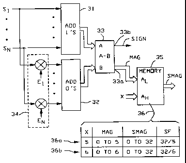
Turning now to Fig. 3, the internal structure of
one preferred embodiment of the digital combiner 11 will be
described. This Fig. 3 embodiment includes a pair of
digital adder circuits 31 and 32, a digital subtractor
CA 02220507 1997-11-07
WO 96/36145 PCT/US96/07741
-9-
circuit 33, a control circuit 34, and a memory circuit 35.
All of these circuits 31 through 35 are interconnected to
each other as shown in Fig. 3.
in operation, the digital adder circuit 31 sums
all of the "1" chips which concurrently occur in the chip
sequences Si through SN. At the same time, the digital
adder circuit 32 sums all of the "0" chips which get passed
through the control circuit 34 and concurrently occur in
the chip sequences. Then the digital subtractor circuit 33
subtracts the sum which is formed by the adder circuit 32
from the sum which is formed by the adder circuit 31. This
produces a MAG signal which occurs on output 33a, and it
also produces the SIGN signal on output 33b. Signal MAG is
a binary representation of the number of "1" chips minus
the number of "0" chips which concurrently occur in the
chip sequences which encode actual data.
For example, the total number of digital input
signals D1 through DN may be thirty-two; but not all thirty-
two input signals need to be present all of the time.
During one time period, only five input signals D1 through
D5 may be present; during another time interval, six input
signals Di through D6 may be present; etc. However, since
the signals D1 through DN only have a"1" and "0" state, it
follows that each of the chip sequences Sl through S. will
always be in a"i" state or a"0" state, even though some
of the digital input signals D1 through DN are not actual
data signals. Accordingly, in order to generate the
correct MAG signal when all digital input signals are not
present, the control circuit 34 is provided.
Within the control circuit 34, each of the chip
sequences Sl through SN is EXCLUSIVE-OR'd with a
corresponding enable signal E1 through EN. When an enable
signal Ei is a"1", all chips in the corresponding chip
sequence Si are inverted before they are sent to the adder
circuit 32. By comparison, if the enable signal Ei is a
"0", then all chips in the corresponding chip sequence Si
are sent to the adder circuit 32 without being inverted.
CA 02220507 1997-11-07
WO 96/36145 PCT/US96/07741
-10-
Each of the chip sequences Si through SN which are
sent to the adder circuit 32 without being inverted will
have their "1" chips added by both of the adder circuits 31
and 32. Consequently, those sums will cancel each other
when they are subtracted by the subtractor circuit 33. As
a result, signal MAG gives just the magnitude of the number
of "1" chips minus the number of "0" chips in the signals
S1 through SN which encode actual data.
Signal MAG is sent to a set of address inputs AL
on the memory 35. At the same time, an externally
generated digital control signal X is sent to another set
of address inputs AH on the memory 35. This control signal
X indicates the total number of chip sequences which encode
actual data and thus need to be combined. For example, X
equals 5 when five chip sequences Sl through S5 encode
actual data; X equals 6 when six chip sequences Si through
S6 encode actual data; etc.
Memory 35 stores multiple linearly scaled
products SMAG of each value of the signal MAG. And, those
linearly scaled products are selectively addressed and read
from the memory 35 by the signals which are sent to the
memory address inputs AL and Ax. This enables the output
signal SMAG, from the memory 35, to be a differently scaled
multiple of the signal MAG depending upon the total number
of chip sequences that are being combined.
For example, when five chip sequences Sl through
S5 are being combined, the signal MAG will vary from 0 to
5. Consequently, in order to make the corresponding output
signal SMAG vary from 0 to 32, the signal MAG times the
scale factor of 32 - 5 is stored'in and read from the
memory. This is indicated in Fig. 3 by the entries in row
36a of a table 36. Similarly, when six chip sequences Sl
through S6 are being combined, the signal MAG will vary from
0 to 6. Thus, in order for the output signal SMAG to
continue to vary from 0 to 32, the signal MAG times the
scale factor of 32 - 6 is stored in and read from the
CA 02220507 1997-11-07
WO 96/36145 PCT/US96/07741
-11-
memory. This is indicated by the entries in row 36b of
table 36.
By keeping the output signal SMAG in a fixed
range (such as 0 to 32) while the maximum magnitude of the
input signal MAG varies, various peak power constraints can
be met. For example, in Fig. 1, the amplifier 12d will
have a peak power limit which must not be exceeded in order
for the amplifier to operate properly. Similarly, the
signals from the antenna 13 will have a peak power limit
which is imposed by a governmental agency such as the FCC.
Now, referring to Fig. 4, the internal structure
of another preferred embodiment of the digital combiner 11
will be described. This Fig. 4 embodiment includes a
digital adder circuit 41, a pair- of digital subtractor
circuits 42 and 43, a control circuit 44, and a memory
circuit 45. All of these components 41 through 45 are
interconnected as shown in Fig. 4.
In operation, the enable circuit 44 selectively
passes the chip sequences S1 through SN to the adder circuit
41. This is achieved by a set of AND gates 44a through 44n
which are included within the control circuit 44. Each of
the AND gates 44a through 44n receives a respective one of
the chip sequences Si and it also receives a corresponding
enable signal Ei, where "i" ranges from 121" to "N". When
the enable signal Ei is a"1", the corresponding chip
sequence Si is passed to the adder 41; whereas when the
enable signal Ei is a"0", the corresponding chip sequence
Si is inhibited from passing to the adder circuit 41.
Adder circuit 41 sums all of the "1" chips that
concurrently occur in the synchronized chip sequences Si
through SN and which are passed through the control circuit
44. That sum is then sent on an output 41a to both of the
subtractor circuits 42 and 43. In the subtractor circuit
42, the sum from the adder circuit 41 is subtracted from
the total number of chip sequences X which encode actual
data. This subtraction operation generates a signal on the
subtractor's output 42a.
CA 02220507 1997-11-07
WO 96/36145 PCT/US96/07741
-12-
Ci.rcuit 43 operates by subtracting the signal on
output 42a from the signal on output 41a. Those two
signals respectively indicate the number of "0" chips and
the number of "1" chips that concurrently occur in the chip
sequences Sl through SN which encode actual data.
Consequently, the signals SIGN and MAG from the subtractor
circuit 43 respectively give the sign and the magnitude of
the number of "1" chips minus the number of "0" chips which
concurrently occur in the signals Si through SN and encode
actual data.
Signal MAG from the subtractor circuit 43 is sent
to a set of address inputs AL on the memory 45; and at the
same time, the externally generated digital control signal
X i.s sent to another set of address inputs AH on the memory
45. This memory 45 is identical to the same as the
previously described memory,35 of Fig. 3. That is, memory
45 stores multiple linearly scaled products of each value
of the signal MAG; and those linearly scaled products are
selectively addressed and read from the memory 45 by the
signals on address inputs AL and AH. Thus, the output
signal SMAG from the memory 45 is a linearly scaled
multiple of the signal MAG with the particular scale
depending upon the total number of chip sequences X that
encode actual data.
Next, with reference to Figs. 5 and 6, still
another preferred embodiment of the digital combiner
circuit 11 will be described. This embodiment has an
internal structure which is shown in Fi.g. 6, and the basis
for the Fig. 6 structure is provided by a set of equations
which are shown in Fig. 5.
Equation eql of Fig. 5 states that the signal MAG
is a multi-bit binary representation of the number of "1"
chips minus the number of "0" chips which concurrently
occur in the chip sequences Si through SN and encode actual
data. Equation eq2 states that the number of "0" chips in
equation eql can be expressed as the total number of chip
sequences X which encode actual data minus the number of
CA 02220507 1997-11-07
WO 96/36145 PCT/US96/07741
-13-
"1" chips in equation eql. Substituting equation eq2 into
equation eql yields equation eq3; and then rearranging the
various terms of equation eq3 yields equation eq4.
Equation eq4 states that the signal MAG equals
twice the number of "1" chips that concurrently occur in
the chip sequences Si through SN which encode actual data
minus the total number of chip sequences X which encode
actual data. This equation eq4 is the basis for the
digital combiner circuit of Fig. 6.
Included in the Fig. 6 embodiment is an adder
circuit 51, a subtractor circuit 52, a control circuit 53,
and a memory circuit 54. All of these components 51
through 54 are interconnected as shown in Fig. 6.
In operation, the encoder circuit 53 passes all
of the chip sequences which encode actual data to the adder
51; and, all other chip sequences which do not encode
actual data are inhibited from reaching the adder 51. This
is achieved by providing the control circuit 53 with the
same internal structure as the previously described control
circuit 44 of Fig. 4.
All of the "1" chips that concurrently occur in
the chip sequences Si through SN and which pass through the
control circuit 53 are added by the adder circuit 51; and
the resulting sum occurs on the adder's output 51a. That
sum from the adder 51 is multiplied by two by appending a
"0" to the least significant bit; and this is indicated by
reference numeral 55 in Fig. 6.
Subtractor circuit 52 subtracts the total number
of chip sequences X which encode actual data from twice the
sum that is formed by the adder circuit 51. Thus,
subtractor circuit 52 carries out the subtraction operation
which is indicated in equation eq4 of Fig. 5.
Consequently, the signals SIGN and MAG from the subtractor
circuit 52 respectively indicate the sign and magnitude of
the number of "1" chips minus the number of "0" chips which
concurrently occur in the chip sequences S1 through S. and
which encode actual data.
CA 02220507 1997-11-07
WO 96/36145 PCT/US96107741
-14-
Signal MAG from the subtractor circuit 52 is sent
to a set of address inputs AL on the memory 54; and at the
same time, the control signal X is sent to another set of
address inputs AH on the memory 54. Here again, the memory
54 is the same as the previously described memories 35 and
45 in that it stores multiple linearly scaled products of
each value of the signal MAG. Those linearly scaled
products are selectively addressed and read from the memory
54 by the signals on the AL and AH address inputs.
Consequently, the output signal SMAG from the memory 54 is
a linearly scaled multiple of the signal MAG with the
particular scale depending upon the total number of chip
sequences X that encode actual data.
Next, referring to Fig. 7, the internal structure
of yet another preferred embodiment of the digital combiner
circuit will be described. This Fig. 7 embodiment includes
an adder circuit 61, a control circuit 62, and a memory
circuit 63. All of these components are interconnected to
each other as shown in Fig. 7.
Control circuit 62 operates in the same manner
and has the same internal structure as the previously
described control circuit 44 of Fig. 4. Thus, the adder 61
only sums the "1" chips which occur in the chip sequences
Si through SN which encode actual data. That sum is
indicated by a signal MAG' which occurs on an output 61a
from the adder 61.
Signal MAG' is sent to a set of address inputs AL
on the memory 63; and at the same time, the externally
generated digital control signal X is sent to another set
of address inputs AH on the memory 63. For each combination
of the signal's MAG' and X, the number of "1" chips minus
the number of "0" chips which concurrently occur in the
chip sequences Sl through S. and encode actual data is given
by equation eq4 of Fig. 5. Thus, at each storage location
which is addressed by the signals X and MAG', the memory 63
stores the corresponding SIGN and SMAG signals. Those
stored signals SIGN and SMAG are selectively addressed and
CA 02220507 1997-11-07
WO 96/36145 PCT/US96/07741
-15-
read from the memory 63 by the signals MAG' and X which are
sent to the memory address inputs AL and AH.
For example, consider the case where only five of
the chip sequences Sl through S5 encode actual data. In
that case, X will be equal to 5 and signal MAG' will have
values of 0, 1, 2, 3, 4 and 5. This is indicated in Fig.
7 by the left-hand column of table 64.
Also in the table 64, the center column shows the
SIGN and MAG signals which correspond to each combination
of the X and MAG' signals. For example, when signal MAG'
equals 4, the chip sequences Si through S5 must contain five
"1" chips and one "0" chip. Consequently, the number of
111" chips minus the number of "0" chips equals +3.
Likewise, when the signal MAG' equals 0, the chip sequences
S1 through S5 must contain no "l" chips and five "0" chips.
Consequently, the number of "1" chips minus the number of
"0" chips equals -5.
Lastly in table 64, the right-hand column shows
the SIGN and SMAG signals which are stored in and read from
the memory 63. In the right-hand column of table 64, the
signal SMAG is obtained by scaling the signal MAG by a
factor of 32 = 5. This particular scale factor is just one
example, since any desired scale factor can be used.
Similarly, when X is equal to 6, the signal MAG'
will have values of 0, 1, 2, 3, 4, 5 and 6. For each
combination of the signal X = 6 and the signal MAG', the
corresponding number of "1" chips minus the number of "0"
chips can be determined by equation 4. That number is then
multiplied by a linear scale factor and the result is
stored in the memory 63 at the storage location which is
addressed by the signals X = 6 and MAG'.
Turning now to Figs. 8, 9, 10 and 11A through
11C, a second electronic transmitter will be described
which is related to the electronic transmitter of Figs. 1-7
but which has a greatly improved characteristic.
Specifically, with the electronic transmitter of Fig. 8,
the signals which are transmitted have a much smaller peak-
CA 02220507 1997-11-07
WO 96/36145 PCT/US96/07741
-16-
to-average power ratio than the signals which are
transmitted by the electronic transmitter of Fig. 1.
Being able to transmit signals with a small peak-
to-average power ratio is desirable because it enables the
transmitted signal to be received at a further distance
without increasing the peak power. As was previously
pointed out, the peak power of the transmitted signal will
be limited by various power constraints, such as those
which are imposed by a governmental agency like the FCC.
And, by transmitting a signal with a low peak-to-average
power ratio, the average power of the transmitted signal is
made large without exceeding the peak power constraint.
in Fig. 8, the electronic transmitter which
transmits signals with a low peak-to-average to power ratio
is shown as including an encoding circuit 70, a digital
combiner circuit 71, a modulator circuit 72, and an
antenna 73. All of these components 70 through 73 are
interconnected to each other as illustrated.
Components 70, 72, and 73 respectively are
identical to the previously described components 10, 12,
and 13 in the Fig. 1 electronic transmitter. By
comparison, the digital combiner circuit 71 in the Fig.
8 electronic transmitter is different; and due to this
difference, the reduced peak-to-average power ratio in the
transmitted signal is obtained.
One preferred embodiment of the digital channel
combiner circuit 71 is shown in Fig. 9. That embodiment
includes components 31, 32, 33, 34 and 80. Components 31
through 34 form the SIGN and MAG signals just like the
components 31 through 34 of the Fig. 3 digital combiner
circuit; and those SIGN and MAG signals respectively
indicate the sign and magnitude of the number of 111" chips
minus the number of "0" chips which concurrently occur in
the chip sequences Sl through SN and encode actual data.
By comparison, component 80 is a memory which
stores multiple non-linearly distorted representations
SDMAG of each value of the signal MAG. Those distorted
CA 02220507 1997-11-07
WO 96/36145 PCT/US96/07741
-17-
representations SDMAG are selectively addressed and read
from the memory 80 by the signals MAG and X which are sent
to the memory address inputs AL and AH.
in Fig. 9, a table 81 is provided which shows an
example of the SDMAG signals that are stored in and read
from the memory in response to the address signals X and
MAG. Those SDMAG signals which are shown in row 82 are
read from the memory 80 when X is equal to five (i.e. -
when a total of five chip sequences S1 through S5 encode
actual data). By comparison, those SDMAG signals which are
shown in row 83 are read from the memory 80 when X is equal
to six (i.e. - when six chip sequences Si through S6 encode
actual data).
in the case where X is equal to 5, the signal MAG
will have values of 1, 3, and 5. To obtain the
corresponding SDMAG signals, the MAG signals of 1, 3 and 5
are non-linearly distorted to 3, 4, and 5. This is
indicated in table 81 by the column labeled DMAG. Then, to
obtain the SDMAG signals which are stored in the memory 80,
the distorted magnitudes DMAG are each multiplied by a
scale factor (such as 32 - 6).
Similarly, when X is equal to 6, the MAG signal
will have values of 0, 2, 4, and 6. To obtain the
corresponding output signals SDMAG, the MAG signals of 0,
2, 4, and 6 are non-linearly distorted to 3, 4, 5 and 6.
This is indicated in table 81 by the column labeled DMAG.
Then, to obtain the SDMAG signals which are stored in the
memory 80, each of the distorted magnitudes DMAG is
multiplied by 32 = 6.
A comparison between the peak-to-average power
ratio of the signals which are transmitted by the Fig. 8
circuit and the signals which are transmitted by the Fig.
1 circuit is shown in Fig. 8. In this comparison, the
number of chip sequences which encode actual data signals
is set to five as one example. Also, to simplify the
calculations, a scale factor of one is assumed. Thus, MAG
equals SMAG and DMAG equals SDMAG.
CA 02220507 1997-11-07
WO 96/36145 PCT/US96/07741
-18-
To begin the comparison, equation eqlO of Fig. 10
gives an expression for the average power in the
transmitted signal from the Fig. 1 circuit. At any one
particular time instant, transmitted si.gnal power will be
proportional to the square of the magnitude of the signal
MAG from the digital combiner circuit 11. For the case
where X is equal to five, signal MAG has magnitudes of 1,
3 and 5. Magnitude 1 occurs for twenty different
combinations of the chip sequences Si through S5; magnitude
3 occurs for ten different combinations; and magnitude 5
occurs for two different combinations. Thus, the average
power in the transmitted signal from the Fig. 1 circuit
may be expressed as shown by term 91 in equation eq10.
Then, to obtain the peak-to-average power ratio, the peak
power is simply divided by the average power from term 91;
and this is performed by equation eqll.
Similarly, equation eq20 of Fig. 10 gives an
expression for average power in the signal which is
transmitted from the transmitter circuit of Fig. 8. Here,
transmitted signal power at any one particular time instant
is proportional to the square of the signal DMAG. For the
case where X is equal to five, signal DMAG has magnitudes
of 3, 4, and 5. Magnitude 3 occurs for twenty different
combinations of the chip sequences Sl through S5; magnitude
4 occurs for ten different combinations and magnitude 5
occurs for two different combinations. Consequently, the
average power in the transmitted signal from the Fig. 8
circuit can be expressed as shown by term 92 in equation
eq20. Then, to obtain the peak-to-average power ratio, the
peak power is divided by the average power as given by the
term 92; and this is performed by equation eq2l.
A comparison of equation eq21 with equation eqll
shows that the peak-to-average power ratio for the Fig. 8
circuit is more than two times smaller than the peak-to-
average power ratio for the Fig. 1 circuit. This is an
important feature since it means that the maximum distance
over which signals from the Fig. 8 circuit can be received
CA 02220507 1997-11-07
WO 96/36145 PCT/US96/07741
-19-
is significantly larger than the maximum distance over
which signals from the Fig. 1 circuit can be received.
All of the calculations which occur in the
equations of Fig. 10 can be repeated for different values
of X. And, such calculations show that as X increases, the
improvement in the peak-to-average power ratio which is
obtained by the Fig. 8 transmitter also increases.
Turning now to Fig. 11A, it illustrates in a
graphical form the relation between the signal MAG and its
distorted representation DMAG for the case where X is equal
to five. There, on a curve 100, three points 100a, 110b
and 100c respectively show that the MAG signal of
magnitudes 1, 3, and 5 are non-linearly distorted to the
DMAG signal of magnitudes 3, 4, and 5. By comparison, if
the signal MAG was simply amplified in a linear fashion to
obtain the DMAG signal, then MAG and DMAG would be
graphically related by a straight line which passes through
the graph's origin 101. Such a line is indicated in Fig.
11A by referenced numeral 102.
It is to be understood, of course, that Fig. 11A
shows just one specific example of the manner in which the
signal MAG may be non-linearly distorted in order to
decrease the peak-to-average power ratio of the transmitted
output signal. Two other examples are shown in Figs. 11B
and 11C.
In Fig. 11B, the relation between the signal MAG
and its non-linearly distorted representation DMAG, is
given by a curve 110 for the case where X is equal to six.
With this distortion, only a portion of the input signal
MAG is distorted in a non-linear fashion; and, that portion
is indicated by reference numeral 110a.
In Fig. 11B, the average power of the DMAG signal
will be larger than the average power of the MAG signal
because the non-linear distortion 110a makes at least some
magnitudes of the DMAG signal larger than the corresponding
magnitudes of the MAG signal. At the same time, the DMAG
CA 02220507 1997-11-07
WO 96/36145 PCT/US96/07741
-20-
signal and the MAG signal have the same peak power because
their peak amplitudes are the same.
In Fig. 11C, the relation between the signal MAG
and its distorted representation DMAG is shown by a curve
120. With this distortion, the distorted output signal
DMAG decreases in magnitude at a variable rate as the
magnitude of the MAG signal varies from a maximum to a
minimum.
In Fig. 11C, the average power of the DMAG signal
will be larger than the average power of the MAG signal
because the variable rate non-linear distortion makes
certain magnitudes of the DMAG signal larger than the
corresponding magnitude of the MAG signal. But here again,
the DMAG signal and the MAG signal have the same peak power
because their peak amplitudes are the same.
One characteristic of the distortion which occurs
in all of the Figs. 11A, 11B, and 11C is that the distorted
output signal DMAG has a maximum magnitude when the signal
MAG is at a maximum magnitude. That maximum DMAG magnitude
divided by the maximum MAG magnitdue defines one particular
gain G. And, a second characteristic of the distortion
which occurs in Figs. 11A-11C is that the distorted signal
DMAG is larger than the signal MAG times the gain G when
the input signal is in a predetermined range below the
maximum magnitude. As longas the MAG and DMAG signals are
related by a non-linear distortion which has these two
characteristics, the DMAG signal wil]. have an improved
peak-to-average power ratio.
Turning next to Figs. 12, 13, 14, and 15A through
15C, a third electronic transmitter will be described which
is related to the electronic transmitters of Figs. 1-lic
but which operates on a different principal. With the
electronic transmitter of Fig. 12, distorted output signals
SDMAG' are again generated which have a small peak-to-
average power ratio in comparison to the MAG signal. But,
the SDMAG' signal is generated with a magnitude which
CA 02220507 1997-11-07
WO 96/36145 PCT/US96/07741
-21-
is proportional to the probability of occurrence of the
corresponding MAG signal.
Thus, the SDMAG' signal has a large magnitude
when the corresponding MAG signal has a high probability of
occurrence even though that corresponding MAG signal may
have a small magnitude. Conversely, the SDMAG' has a small
magnitude when the corresponding MAG signal has a low
probability of occurrence even though that corresponding
MAG signal may have a large magnitude.
in Fig. 12, the electronic transmitter which
operates on the above-principal is shown as including an
encoding circuit 130, a digital combiner circuit 131, a
modulator circuit 132, and an antenna 133. All of these
components 130 through 132 are interconnected to each other
as illustrated.
Each of the components 130, 132, and 133
respectively is identical to the previously described
components 10, 12, and 13 of the Fig. 1 electronic
transmitter. By comparison, the digital channel
combiner 131 in the Fig. 12 electronic transmitter is
different in that it generates the signal SDMAG'.
One preferred embodiment of the digital channel
combiner circuit 131 is shown in Fig. 13. That embodiment
includes components 31, 32, 33, 34 and 140. Components 31
through 34 form the SIGN and MAG signals just like the
components 31 through 34 of the Fig. 3 digital combiner
circuit; and those SIGN and MAG signals respectively
indicate the sign and magnitude of the number of "1" chips
minus the number of "0" chips that concurrently occur in
the chip sequences S1 through SN which encode actual data.
By comparison, component 140 is a memory which
stores multiple non-linearly distorted representations
SDMAG' of each value of the signal MAG. Those distorted
representations SDMAG are selectively addressed and read
from the memory 140 by the signals MAG and X which are sent
to the memory address inputs AL and A.H.
CA 02220507 1997-11-07
WO 96/36145 PCT/US96/07741
-22-
in Fig. 13, a table 141 is provided which shows
an example of the SDMAG' signals which are stored in and
read from the memory 141 in response to the address signals
X and MAG. Those SDMAG' signals which are shown in row 142
are read from the memory 140 when a total of five chip
sequences Sl through S5 encode actual data; and those SDMAG'
signals which are shown in row 143 are read from the memory
140 when six chip sequences Si through S6 encode actual
data.
in the case where X is equal to five, the signal
MAG will have magnitudes of 1, 3, and 5. Magnitude 1
occurs for twenty different combinations of the chip
sequences S1 through S5; magnitude 3 occurs for ten
different combinations; and magnitude 5 occurs for only two
different combinations. Thus, the probability of
occurrence for MAG=1 is 20/32; the probability of
occurrence for MAG=3 is 10/32; and the probability of
occurrence for MAG=5 is 2/32. This is indicated in table
141 by the column labeled PROB.
To obtain the SDMAG' signals, their magnitudes
are made large when the probability of occurrence of the
corresponding MAG signals is large; and vice-versa. This
is indicated in table 141 by the column labeled DMAG'.
Then, to obtain the SDMAG' signals which are stored in the
memory 140, the distorted magnitudes DMAG' are each
multiplied by a scale factor (such as 32 = 5).
Similarly, when X is equal to six, the MAG signal
will have values of 0, 2, 4, and 6. Magnitude 0 occurs for
twenty different combinations of the chip sequences Si
through S6; magnitude 2 occurs for thirty different
combinations; magnitude 4 occurs for twelve different
combinations; and magnitude 6 occurs for two different
combinations.
Accordingly, to obtain the corresponding output
signals SDMAG, the MAG signals of 0, 2, 4, and 6 are non-
linearly distorted to 6, 5, 4 and 3. This is indicated in
table 141 by the column labeled DMAG'. Then, to obtain the
CA 02220507 1997-11-07
WO 96/36145 PCTIUS96/07741
-23-
SDMAG' signals which are stored in the memory 140, each of
the distorted magnitudes DMAG' is multiplied by 32 = 8.
A calculation of the peak-to-average power ratio
of the signals which are transmitted by the Fig. 12 circuit
is shown in Fig. 14. In this calculation, the number of
chip sequences which encode actual data signals is set to
five, and the scale factor is set equal to one. Thus,
DMAG' equals SDMAG'.
To begin the calculation, equation eq30 of Fig.
14 gives an expression for the average power in the signal
DMAG'. At any one particular time instant, transmitted
signal power will be proportional to the square of the
magnitude of the signal DMAG'. For the case where X is
equal to five, signal DMAG' has magnitudes of 5, 4 and 3.
Magnitude 5 occurs for twenty different combinations of the
chip sequences S 1 through S5; magnitude 3 occurs for ten
different combinations; and magnitude 5 occurs for two
different combinations. Thus, the average power in the
transmitted signal from the Fig. 14 circuit is expressed by
the term 151 in equation 14. Then, the peak-to-average
power ratio is obtained by dividing the peak power with the
average power from term 151; and this is performed by
equation eq3l.
A comparison of equation eq3l with equation eqil
of Fig. 9 shows that the peak-to-average power ratio for
the Fig. 12 circuit is more than four times smaller than
the peak-to-average power ratio for the Fig. 1 circuit.
Consequently, the maximum distance over which signals from
the Fig. 12 circuit can be received is more than four times
the maximum distance over which signals from the Fig. 1
circuit can be received.
All of the calculations which occur in of Fig. 14
can be repeated for different values of X. And, such
calculations show that as X increases, the improvement in
the peak-to-average power ratio which is obtained by the
Fig. 12 transmitter also increases.
CA 02220507 1997-11-07
WO 96/36145 PCT/US96/07741
-24-
Turning now to Fig. 15A, it illustrates in a
graphical form the relation between the signal MAG and its
distorted representation DMAG' for the case where X is
equal to five. There, a curve 160 has three points 160a,
160b and 160c which respectively show that magnitudes 1, 3,
and 5 of the MAG signal are non-linearly distorted to
magnitudes 5, 4, and 3 of the DMAG' signal. By comparison,
if the signal MAG was simply amplified in a linear fashion
to obtain the DMAG' signal, then MAG and DMAG' would be
graphically related by the straight line 102 which passes
through the graph's origin 101.
Two additional examples of how the signal MAG may
be non-linearly distorted in order to decrease the peak-to-
average power ratio of the transmitted output signal are
shown in Figs. 15B and 15C. In Fig. 15B, the relation
between the signal MAG and its non-linearly distorted
representation DMAG' is given by a curve 170. With this
distortion, signal DMAG' decreases in magnitude at a
variable rate as the signal MAG varies from a minimum to a
maximum. By comparison, in Fig. 15A, the distorted signal
DMAG' decreases in magnitude at a constant rate as the
signal MAG varies from a minimum to a maximum.
Note that the distortion which occurs in Fig. 15A
and Fig.15B is in one respect just the opposite of the
distortion which occurs in Fig. 11A, Fig. 11B, and
Fig. 11C. In Fig. 15A and Fig. 15B, the distorted signal
DMAG' monotonically decreases in magnitude as signal MAG
varies from a minimum to a maximum; whereas in Fig. 11A,
Fig. 11B, and Fig. 11C, the distorted signal DMAG
monotonically decreases in magnitude as signal MAG varies
from a maximum to a minimum.
In Fig. 15B, the average power of the DMAG'
signal will be larger than the average power of the MAG
signal because the non-linear distortion 170 makes the
magnitudes of the DMAG' signal large when the corresponding
magnitudes of the MAG signal occur frequently. At the same
CA 02220507 1997-11-07
WO 96/36145 PCT/US96/07741
-25-
time, the DMAG' signal and the MAG signal have the same
peak power because their peak amplitudes are the same.
in Fig. 15C, the relation between the signal MAG
and its distorted representation DMAG' is shown by a set of
four dots 180. With this distortion, the distorted output
signal DMAG' increases in magnitude and then decreases in
magnitude as the MAG signal varies from a minimum to a
maximum. Signal DMAG' respectively has magnitudes of 5, 6,
4, and 3 when the MAG signal has magnitudes of 0, 2, 4 and
6. This corresponds to the distortion which is shown in
the Fig. 13 table at row 143.
in Fig. 15C, the average power of the DMAG'
signal will be larger than the average power of the MAG
signal because the non-linear distortion 180 makes the
magnitudes of the DMAG' signal large when the corresponding
magnitude of the MAG signal occur frequently. And here
again, the DMAG' signal and the MAG signal have the same
peak power because their peak amplitudes are the same.
A characteristic of the distortion which occurs
in all of the Figs. 15A, 15B, and 15C is that the distorted
output signal DMAG' has its largest magnitude when the
signal MAG has a magnitude which occurs most frequently.
That peak magnitude of the DMAG' signal can occur when the
MAG signal is at a minimum, such as in Figs. 15A and 15B;
or it can occur when the MAG signal is between a maximum
and a minimum, such as in Fig. 15C.
To recover the data bits which are encoded in the
distorted signals from the transmitters of Figs. 8 and 12,
those distorted signals are sent through a receiver circuit
that has a gain which is the inverse of the gain with which
the distorted signals are generated. By this operation,
the undistorted MAG signal is regenerated. Then, from the
undistorted MAG signal, the digital input signals D1 through
, DN are recovered in a conventional fashion, as is taught,
for example, in U.S. patent 5,031,173 entitled "Decoder For
Added Asynchronous Bit Sequences" by R. short, C.
CA 02220507 1997-11-07
WO 96/36145 PCT/US96/07741
-26-
Rushforth, and Z. Xie and which is assigned to the assignee
of the present invention.
An example which illustrates how the undistorted
MAG signal is regenerated from the distorted DMAG' signal
is shown in Fig. 16. There, the column which is labeled
MAG shows signal magnitudes of 1, 3, and 5; and the column
which is labeled DMAG' lists corresponding signal
magnitudes of 5, 4, and 3. This is identical to the
distortion which is shown in Fig. 15A.
Also, in Fig. 16, the colvmn which is labeled G
shows the gain by which the signal MAG must be multiplied
by in order to obtain the distorted signal DMAG'. Further,
the column which is labeled IG shows the inverse gain by
which the distorted signal DMAG'-must be multiplied in
order to regenerate the original MAG signal. That inverse
gain which is shown in the IG column is the gain which is
applied by the receiver circuit in order to regenerate the
MAG signal.
Various preferred embodiments of the invention
have now been described in detail. in addition, however,
many changes and modifications can be made to the details
of these preferred embodiments without departing from the
nature and spirit of the invention.
For example, all of the components 31-34 in the
digital combiner circuit of Fig. 9 can be replaced with
components 41-44 of Fig. 4, or components 51-53 of Fig. 6
or components 61-62 of Fig. 7. Similarly, all of the
components 31-35 in the digital combiner circuit of Fig. 13
can be replaced with components 41-44 of Fig. 4, or
components 51-53 of Fig. 6, or components 61-62 of Fig. 7.
Also, as another modification, the distortion
which was described in conjunction with Figs. 11A-11C and
Figs. 15A-15B may also be applied to an analog input
signal. For example, in Fig. 11A, the signal MAG can be an
analog input signal which has a magnitude that varies
continuously from 0 to 5; and the signal DMAG can be an
analog output signal which has a magnitude that various
CA 02220507 1997-11-07
WO 96/36145 PCT/US96/07741
-27-
continuously from 3 to 5. To generate the analog signal
DMAG, the analog signal MAG is simply multiplied by a gain
which is given by the curve 100.
Similarly, in Fig. 15A, the signal MAG can be an
analog input signal which varies continuously from 0 to 5;
and the signal DMAG' can be an analog output signal which
varies continuously from 3 to 5.5. Such an analog DMAG'
signal is generated by multiplying an analog MAG signal
with a gain which is given by the curve 160.
Accordingly, it is to be understood that the
present invention is not limited to just the details of the
illustrated preferred embodiments but is defined by the
appended claims.