Note: Descriptions are shown in the official language in which they were submitted.
~ CA 02220605 1997-11-27
~ 13-789 94-SM6-360
ION SOURCE BLOCK ~ILAMENT
WlT~ LABYRINT~ CONDUCTIVE PAT~I
Field of the Invention
The present invention relates to a fil~mr.nt for ioni7ing source m~tçri~l~ in anarc c~mhPr of an ion impl~nt~ti~m app~lus and, more particularly, to a fil~mr.ntc~mrri~ing a tlm~trn block having two spiral slits forming a labyrinth conductive
path.
Background of the Invention
One known technique for introducing dopants into a semiconductor wafer
involves directing a beam of ions along a path of travel and selectively po~itioning
0 silicon wafers to i.. l~ .~cl the ion beam. This technique has been widely used in ion
imp1~nt~ti~-n ap~~ ses to dope wafers with controlled cnnrçntr~tic)n~ of an ionized
dopant m~tçri~l
One example of a cnmmçrcial ion impl~nt~tion app~lus is the Eaton model
NV 20 Tmrl~nter. The Eaton impl~nt~tion a~pal~lus comrri~es an ion beam source
~r.mbly inr,hl-ling an arc cll~m~t de.fining an interior region into which controlled
cnn~-~ntr~ti--ns of gas~us source m~trr~ inr~hltling ionizable gas (e.g., oxygen) and
v~rori7ed dopant m~tçri~ls (e.g., arsenic) are injected. A cover plate or e~tractir~n
mrmhçr overlies an open side of the arc ch~mb~r. The ext~action member include.san elliptical opening or arc slit through which ionized molecules escape the arc2 0 chamber interior region.
A cathode c~-mrri.cing a fil~mrnt is disposed in the arc ch~mher. The fil~mçnt
is energized elevating its temperature to emit electrons into the arc chamber interior
region. The electrons collide with the source m~tçri~l gas molecules, yielding energy
) CA 02220605 1997-11-27
to iol~ize the molecules. Ioni_ed moleclllP~ ecc~ring the arc ch mber interior region
through the arc slit are accPler~tP~l along a path of travel thereby forrning an ion beam
which intPrsectc target wafers at an i...~ alion station and implants the wafers with
ionized dopant molecules. An ion source assembly ufili7ing a cath~e fil~mPnt is
~ sPd in U.S. Patent No. 4,714,834 to Shubaly, which is ~cci~P~l to the ~ssignPeof the pre~nt invention.
In prior art ion implqntPts~ the cath~e fil~mPnt typically comrrices a single
loop of tllngstpn wire. An electric polenl,al is applied across the fil~m~nt to heat it
to a thP.rmionic Pmi~sion te...l~n~, wllel~;in free electrons are emitted by thelo fil~mPnt The ;c-ni7~fic)n of ga~eolls source m~teri~lc in the arc chamber interior
region gpnp~t~tes a plasma of highly ionized gas having nearly equal numbers of ions
and electrons. The density of the ions and electrons is such that the so-called Debye
shiP,kling length is much smaller than the ~limpncions of the fil~mPnt The Debye~hiel-ling length is a ch~t~ctptictic ~i~stance in a gaseous source m~tPri~l plasrna
beyond which the electric field of a chalg~ particle is chieldecl by particles having
chalges of the o~osile sign. Only that portion of the filampnt~ perpendicular to a
m~nPtic field impressed on the arc ch~m~Pr, actually undergoes thprmionic çmicsion
~ e it is i~ -.~l in the g~cP~ouc source m~tPrial plasma, ion ~ull~ g occurs
over the entire outer surface of the energized filamP.nt The sputtering action erodes
the entire outer surface of the fil~ment and nltim~tely causes it to fail.
- CA 02220605 1997-11-27
Sw~ of the Invention
A fil~mPnt block or plate for th~rmioni~ ly emitt ng electrons is disposed in
an interior region of an arc ch~mh~t. The arc ch~mher, in turn, is disposed in an
evacuated interior region of an ion source housing. The plate is made of tlmg~enIonizable gaseous source m~teri~le are iniecte(l into the interior region of an arc
ch~mher of the source. The fi1~m~ont plate is energized to a thlo.rmionic emieeion
te~ dLwe that causes electrons to strike the ionizable gaseous source m~t.o.ri~1 and
generate a plasma of source ions. A plerell~d fi1~m~nt plate inClu~ee two spacedapart spiral slits cut through a width of the plate. The slits are cubst~nti~11y parallel
to each other over a portion of their l~ecLive lengths and each slit t~rmin~tçs near
a center region of the plate. The slits form a labyrinth spiraled conductive path for
th.ormionic heating of the plate.
The slits are ch~r~ct~ri7ed by a gap, which is the perpendicular ~ et~nce
between side wall surfaces dçfining the slit. Each slit has a substantially ul~ llll gap
width over the length of the slit. Further, the two slits have gaps which are
snbst~nti~11y equal. For each slit, the gap width is preferably not greater than ten
times the Debye ehie1-1ing length of the charged source m~te.ri~1 plasma. Such a slit
gap width quickly ~llç~ es the energy of the energized plasma enterinP the slit so
erosion of the fi1~ment plate interior wall sl1rf~ces defining the slits by the plasma is
... ;I~;.. i7~
The fi1~m~nt plate includes two spaced apart openings near opposite ends of
the plate. Conductive posts for energi_ing the fi1~ment block extend through apel~wes
in a side wall of the source bounding an arc chamber. An ineu1~tor disposed within
each a~llure isolates the conductive posts from the arc chamber side wall. A
CA 02220605 1997-11-27
.~t.~ difference is applied across the conductive posts c~n~ing a current to flow
through the fil~mP.nt plate along the labyrinth spiraled con~luctive path defined by the
slits. The top surface of the fil~m~.nt plate is po~iti~-nP~l within the arc chamber such
that the top surface is perpendicular to a m~gnp~tic field i~ G~ed on the arc chamber
by an el~Llo~ gnP.t located outside the ion source.
When the fil~m~.nt plate is energized and heated to the thP.rmionic e.mi~ion
t~ ?elalule, free electrons are emitted into an interior region of the arc chamber. A
top surface of the fil~mP.nt plate provides a large, efficient surface for thP.rmionic
e.mi~ic.n superior to the prior art looped wire fil~me.nt
One object of the present invention is to provide a source m~tP.ri~l inni7.ing
fil~mP.nt for use in an ion impl~nt~qfion a~us wherein the fil~ment has an
increased useful life.
Another object of this invention is to provide a fil~mP.nt wherein ~ e.;
erosion is limited to an area that is less than an entire surface area of the fil~mP.nt.
Yet another object of this invention is to provide a fil~ment wherein the
thermiollic emi~ion area is large providing for efficiçnt ioni7~tion of source m~teri~l.
These and other objects, advantages and fealul~ s of the invention will become
better lm~lp~rstood from a detailed descrirti~n of a pl~;relled embodiment of the
invention which is described in conjunction with the ~cc~rnp~nying drawings.
Brief Deseli~tion of the Drawings
Figure 1 is a srhPm~tic pel~ti~/e view of a portion of an ion beam source
~se.mbly of an ion implanter;
Figure 2 is a section~l view of an ion beam source assembly;
~ ~ CA 02220605 1997-11-27
Figure 3 is a top plan view an arc ch~mker inr.lurling a fil~m~.nt plate of the
present invention;
Figure 4 is a view partly in elevation and partly in section of the arc chamber
of Figure 3 as seen from a plane indicated by the line 4-4 in Figure 3;
Figure S is a perspective view of the fil~mrnt plate of Figure 3;
Figure 6 is a top plan view of the fil~ment plate of Figure 3;
Figure 7 is a side elevation view of the plate fil~mPnt of Figure 3 as seen froma plane intlirAted by line 7-7 in Figure 6;
Figure 8 is an elevation view of the plate fil~mr.nt of Figure 3 as seen from a
plane indir~ted by line 8-8 in Figure 6;
Figure 9 is a perspective view of a second embodiment of a fil~ment plate of
the present invention;
Figure 10 is a top plan view of the fil~mpnt plate of Figure 9;
Figure 11 is a side elevation view of the fil~mPnt plate of Figure 9 as seen
from a plane in-lir~ted by the line 11-11 in Figure 10; and
Figure 12 is a front elevation view of the fil~mrnt plate of Figure 9 as seen
from a plane in-1ir~te 1 by the line 12-12 in Figure 10.
~ CA 0222060~ 1997-11-27
Detailed Description
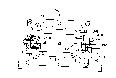
Turning to the drawings, an ion beam source assembly of an ion implanter is
shown generally at 10 in Figures 1 and 2. The ion beam source a~se.mbly 10 inrludes
a cube-shaped ion source housing 12. The ion source housing 12 is made of
~l"~"il~"~" and has an interior cavity 14 which is evacuated by pumps (not shown)
when the ion beam source ~embly is in operation. An arc chamber 62 is supported
within the ion source housing 12. The arc chamber 62 has a base 64 and side walls
66 ~.Yt~.n~ling from the base. The side walls 66 and base 64 define an interior region
68. Source m~te.ri~l~, which, when energized, generate an ion plasma, are routed into
o the arc chamber interior region 68. An open side of the arc chamber 62 is overlaid
by an extraction member 60. Ion genetate~l in the arc ch~m~.r 62 exit through the a
slit 70 in the ~Ytr~ction mP.mber 60 and are shaped into an ion beam by ion beam~haring extraction electrodes 38. The ion beam exits the ion source housing 12
through an opening 18 in a housing wall 28.
Dis~osed within the arc chamber interior region 68 are a fil~m~.nt plate 80 of
the present invention and an electron repeller plate 82. The fil~ment plate 80 is heated
to a th~.rmionic Pmi~sic-n t~.~n~ e by an electric current flowing through the plate
from a conductive post 106 to a c~n~ ctive post 108 to emit free electrons. The
fil~mP.nt block 80 is placed at a negative potential relative to the arc chamber 62, this
2 o accelel~les the emitted electrons which collide with ioni7~ble gaseous source m~teri~l~
injected into the arc ch~mbet interior region 68. The electron - source m~t.o.ti~l
colli~ions result in ionization of the source materials. The repeller plate 82 is
negatively charged to repel electrons gener~ted by the filament plate 80 to minimi7e
the loss of electrons. The gaseous source m~teti~l~ to be ionized are injected into the
~ CA 02220605 1997-11-27 ')
arc ch~mher interior region 68 through a gas inlet a~lLule 84 through which a source
m~t~ri~l tube 85 (Figure 2) .oYt~nA~;
Turning to Figures ~-7, the fil~m.q.nt plate 80 is comrtiseA- of tlmg~ten and, as
best seen in Figure 6, is configured in the shape of an i~oscel~s triangle with rounded
cotnPrs. Two spiral cuts or slits 96, 98 are cut through the width W of the fil~m~nt
plate 80. Preferably, the slits 96, 98 are made in the fil~m~nt plate 80 using a wire
EDM (electron discharge m~rhining) method, well known to those sldlled in the art.
The slits 96, 98 extend from the side walls 92, 94 respectively and spiral inwardly at
increasingly tighter radii toward a c-mml n center region C of the fil~mçnt plate 80.
0 As can best be seen in Figure 6, the slits 96, 98 overlap and are parallel over most of
their respective lçn~hs A gap width or normal ~list~nt e between opposing interior
wall snrf~s of the fil~m.ont plate 80 clçfining each slit 96, 98 is u~ along thelength of the slit. Moleovel, the gap width is subst~nti~lly the same for each slit.
Snit~ble ~lim.on~ion~ for a length L1 of the short side walls 90, 92 and a length L2 of
the long side wall 94, a width W of the fil~mP.nt plate 80 and a gap width are as
follows:
DimP.nsion
L1 (Length of short side walls 90, 92) 1.2 cm.
L2 (Length of long side wall 94) 2.0 cm.
W (Width of fil~m~nt plate 80) 0.3 cm.
Gap width r~ nce of each slit 96, 98 0.3 mm.
The fil~m~.nt plate 80 inclu(le~ two throughbores spaced inwardly from
corners 100, 102. The pair of spaced apart con(luctive posts 106, 108 are press fit into
respective openings. As can best he seen in Figures 3 and 4, the fil~mP.nt plate 80 is
~ CA 02220605 1997-11-27
p~itir~n~d in the arc chamber inteAor region 68 spaced from the side wall 66 andcriP.nted such that a top surface 110 of the fil~m~nt plate is subst~nti~lly parallel to
the side wall which also support the repeller plate 82. The c~n-luctin~ posts 106, 108
extend through a pair of aligned holes in the arc chamber side wall 66. Insulators 109
are sandwiched between the cc nflllctive posts 106, 108 and the side wall openings to
in~ te the arc rh~mhe- 62 from the cnn~ucting posts. A protective plate 107 is
posititn~1 on the c~-n~ ctive posts 106, 108 between the in~ul~tors 109 and the
fil~mP.nt plate 80. The protective plate 107 ple~n~ met~llic deposition on the
in~ll~t--rs 109.
Two power feeds 88 (one of which can be seen in Figure 2) are connected to
the con~luctive posts 106, 108. When the power feeds 88 are energized, a currentflows through the plate 80 along a spiraled labyAnth path I (Figure 6). Where the slits
96, 98 overlap, the current path I has a subst~nti~lly c~ t width from an outer
portion of the fil~m.q.nt plate 80 to the c~mm~n center region C, that is, a sp~cine
~l-.~n adjacent slits as measured along a radius
.Yt~.n~ling oulwaldly from the common center region C is subst~nti~lly c. n~t~ntThe current flow I through the fil~m~.nt plate 80 is suitably adjusted to raise
the tf- ~pr~a~ of the plate to the thP.rmionic ~.mi~ion te~ ~,'al--,~ cau~ing the plate
to emit free electrons. A top surface 110 (Figure 6) of the fil~ment plate 80 provides
a large, efficient surface for thermionic ~.mi~sion
Preferably, the gap width of the slits 96, 98 is not substanti~lly greater than ten
times a Debye shi~ ing length of a charged plasma generated from typical source
m~teri~l.c injected into the arc ch~mber interior region 68. Debye shielding lengths
for plasma having arsenic, phosphorous or antimony source materials range between
~ CA 02220605 1997-11-27
0.1 to 0.5 millimetP,rs (mm.). Thus, the pre~ell~,d gap width of 0.30 mm. is not greater
than ten times the Debye shielding length of even a plasma with a 0.1 mm. Debye
shielding length. Such a slit gap width is so narrow that an energi_ed plasma cannot
be sust~in~A in the gap, that is, the energy of the energi_ed plasma çntçring the slits
96, 98 is quicldy ~ttPn-l~ted so that plasma erosion of the interior wall snrf~ces of the
fil~mP,nt plate 80 dP,fining each slit 96, 98 is minimi7ed
Erosion by splltt-pring is subst~nti~lly limited to the top surface 110 of the
fi1~ment plate 80. Sp~ltte,ring does not occur on a bottom surface 112 of the fil~mPnt
plate 80 because a volume of the arc ~ mher interior region 58 defined between the
fil~m.~nt plate bottom surface 112 and the region of the arc ch~mhpr side wall 66
through which the conductive posts 106, 108 extend is too small to sustain a pl~m~,
Figures 9-11 illustrate an ~lt,Pm~tP, embodiment of the fil~mPnt plate of the
present invention. The fil~mPnt plate 120 is generally rectangular in profile and has
rounded corners. The fil~mpnt plate 120 inchl(les two spiral slits 122, 124 through a
width W' of the plate. The slits 122, 124 extend from respective side walls 126, 128
and spiral toward a center region C of the fil~mP,nt plate 120. As can best be seen in
Figure 10, the slits 122, 124 overlap and are parallel over most of their respective
len~hs. A gap width or normal t~ nce b~ ,ell opposing interior wall sllrf~ces ofthe fil~mP,nt plate 120 (lefining each slit 122, 124 is u~ ulm along the length of the
slit. Mor~o~er, the gap width is subs~nti~lly the same for each slit. Suitable
~limP,n~ion~ for a length Ll' of the short side walls 126, 128 and a length L2' of the
long side walls 132, 134, the width W' of the fil~ment plate 120 and the gap width are
as follows:
) CA 02220605 1997-11-27
Dimension
Ll' 1.5 cm.
L2' 2.0 cm.
W' 0.3 cm.
Gap width tli~t~nce of each slit 122, 124 0.3 mm.
The fil~m.o.nt plate 120 in~ludes two throughbores spaced inwardly from side
walls 126, 128. A pair of spaced apart conductive posts 140, 142 are press fit into
~pec~ opçnings. The power feeds 88 are co~ ecled to the conductive posts 140,
142. When the power feeds 88 are energized, a current flows through the plate 120
along a spiraled labyrinth path r (Figure 10).
A m~gnit~lde of the current r through the fil~ment plate 120 is suitably
adjusted to raise a temperature of the plate through which the current r flows to the
thlo.rmic~nic .o.mi~i-n te~ e causing the plate to emit free electrons. A top
surface 144 of the fil~m~nt plate 120 provides a large, efficie.nt surface for th~ormi~nic
emissic~n
The gap width of the slits 122, 124 is not subst~nti~lly larger t-h~n ten times
the Debye .~hiPl~ling length of a charged plasma gçnçrRted from typical source
m~teri~l~ injected into the arc ch~mher interior region 68. This minimi7es po.nçtr~tiQn
of the energi_ed plasma into the gaps of the slits 122, 124 and, thus, minimi7l~s
2 o erosion of the interior wall surf~ces de-fining the slits. As noted with respect the first
embo~ ..çl~l, erosion by sputte.ring is subst~nti~lly limited to the top surface 144 of
the fil~mçnt plate 120. SputtP.ring does not occur on a bottom surface 144 of the
fil~mçnt plate 120 b~use a volume of the arc ch~mber interior region 58 defined
~h.e~n the fil~m~nt plate bottom surface 144 and the region of the arc chamber side
. '~ CA 0222060~ 1997-11-27 '!
11
wall 66 through which the contluctive posts 140, 142 extend is too small to sustain a
plasma.
The present invention has been described with a degree of particularity, but it
is the intent that the invention include all m~lifiç~tic)n~ from the ~ii~,lQse~ plGfe,led
design failing within the spirit or scope of the appended claims.