Note: Descriptions are shown in the official language in which they were submitted.
CA 02220740 2001-03-19
SYMBOL DECODING APPARATUS WITH PLURAL DATA SLICERS AND
AN ADAPTIVE NTSC CO-CHANNEL INTERFERENCE FILTER
FIELD OF THE INVENTION
The present invention relates to digital television systems, such as the
digital
high-definition television (HDTV) system used for terrestrial broadcasting in
the
United States of America in accordance with the Advanced Television
Sub-Committee (ATSC) standard, and more particularly, to digital television
receivers
with adaptive filter circuitry for suppressing co-channel interference from
analog
television signals, such as those conforming to the National Television
Systems Committee (NTSC) standard.
BACKGROUND OF THE INVENTION
A Digital Television Standard published 16 September 1995 by the Advanced
Television Subcommittee (ATSC) specifies vestigial sideband (VSB) signals for
transmitting digital television (DTV) signals in 6-MHz-bandwidth television
channels
such as those currently used in over-the-air broadcasting of National
Television
Subcommittee (NTSC) analog television signals within the United States. The
VSB
DTV signal is designed so its spectrum is likely to interleave with the
spectrum of a
co-channel interfering NTSC analog TV signal. This is done by positioning the
pilot
carrier and the principal amplitude-modulation sideband frequencies of the DTV
signal at odd multiples of one-quarter the horizontal scan line rate of the
NTSC analog
TV signal that fall between the even multiples of one-quarter the horizontal
scan line
rate of the NTSC analog TV signal, at which even multiples most of the energy
of the
luminance and chrominance components of a co-channel interfering NTSC analog
TV
signal will fall. The video carrier of an NTSC analog TV signal is offset 1.25
MHz
from the lower limit frequency of the television channel. The carrier of the
DTV
CA 02220740 1998-06-25
signal is offset from such video carrier by 59.75 times
the horizontal scan line rate of the NTSC analog TV
signal, to place the carrier of the DTV signal about
309,877.6 KHz from the lower limit frequency of the
television channel. Accordingly, the carrier of the DTV
signal is about 2,690122.4 Hz from the middle frequency of
the television channel.
The enact symbol rate in the Digital Television
Standard is (684/286) times the 4.5 MHz sound carrier
offset from video carrier in an NTSC analog TV signal.
The number of symbols per horizontal scan line in an NTSC
analog TV signal is 684, and 286 is the factor by which
horizontal scan line rate in an NTSC analog TV signal is
multiplied to obtain the 4.5 MHz sound carrier offset from
video carrier in an NTSC analog TV signal. The symbol
rate is 10.762238 megasymbols per second, which can be
contained in a VSB signal extending 5.381119 MHz from DTV
signal carrier. That is, the VSB signal can be limited to
a band extending 5.690997 MHz from the lower limit
frequency of the television channel.
The ATSC standard for digital HDTV signal
terrestrial broadcasting in the United States of America
is capable of transmitting either of two high-definition
television (HDTV) formats with 16:9 aspect ratio. One
HDTV display format uses 1920 samples per scan line and
1080 active horizontal scan lines per 30 Hz frame with 2:1
field interlace. The other HDTV display format uses 1280
luminance samples per scan line and 720 progressively
scanned scan lines of television image per 60 Hz frame.
The ATSC standard also accommodates the transmission of
DTV display formats other than HDTV display formats, such
as the parallel transmission of four television signals
having normal definition in comparision to an NTSC analog
television signal.
2
' ' CA 02220740 1998-06-25
DTV transmitted by vestigial-sideband (VSB)
amplitude modulation (AM) during terrestrial
broadcasting in the United States of America comprises
a succession of consecutive-in-time data fields each
containing 313 consecutive-in-time data segments. The
data fields may be considered to. be consecutively
numbered modulo-2, with each odd-numbered data field
and the succeeding even-numbered data field forming a
data frame. The frame rate is 20.66 frames per
second. Each data segment. is of 77.3 microseconds
duration. So, with the symbol rate being 10.76 MHz
2a
CA 02220740 1997-11-10
there are 832 symbols per data segment. Each segment of data begins with a
line
synchronization code group of four symbols having successive values of +S, -S,
-S
and +S. The value +S is one level below the maximum positive data excursion,
and
the value -S is one level above the maximum negative data excursion. The
initial line
of each data field includes a field synchronization code group that codes a
training
signal for channel-equalization and multipath suppression procedures. The
training
signal is a 511-sample pseudo-noise sequence (or "PN-sequence") followed by
three
63-sample PN sequences. The middle ones of the 63-sample PN sequences in the
field
synchronization codes are transmitted in accordance with a first logic
convention in
the first line of each odd-numbered data field and in accordance with a second
logic
convention in the first line of each even-numbered data field, the first and
second
logic conventions being one's complementary respective to each other.
The data within data lines are trellis coded using twelve interleaved trellis
codes, each a 2/3 rate trellis code with one uncoded bit. The interleaved
trellis codes
are subjected to Reed-Solomon forward error-correction coding, which provides
for
correction of burst errors arising from noise sources such as a nearby
unshielded
automobile ignition system. The Reed-Solomon coding results are transmitted as
8-level (3 bits/symbol) one-dimensional-constellation symbol coding for over-
the-air
transmission, which transmissions are made without symbol preceding separate
from
the trellis coding procedure. The Reed-Solomon coding results are transmitted
as
16-level (4 bits/symbol) one-dimensional-constellation symbol coding for
cablecast,
which transmissions are made without preceding. The VSB signals have their
natural
carrier wave, which would vary in amplitude depending on the percentage of
modulation, suppressed.
The natural carrier wave is replaced by a pilot carrier wave of fixed
amplitude,
which amplitude corresponds to a prescribed percentage of modulation. This
pilot
carrier wave of fixed amplitude is generated by introducing a direct component
shift
. into the modulating voltage applied to the balanced modulator generating the
amplitude-modulation sidebands that are supplied to the filter supplying the
VSB
signal as its response. If the eight levels of 4-bit symbol coding have
normalized
values of -7, -5, -3, -1, +1, +3, +5 and +7 in the carrier modulating signal,
the pilot
CA 02220740 1997-11-10
carrier has a normalized vale of 1.25. The normalized value of +S is +5, and
the
normalized value of -S is -5.
In the earlier development of the DVT art it was contemplated that the DTV
broadcaster might be called upon to decide whether or not to use a symbol
precoder at
the transmitter, which symbol precoder would follow the symbol generation
circuitry
and provide for precoded filtering of symbols. This decision by the
broadcaster would
have depended upon whether interference from a co-channel NTSC. broadcasting
station were expected or not. The symbol precoder would complement the symbol
postcoding incidentally introduced in each DTV receiver by a comb filter used
before
the data-dicer in the symbol decoder circuitry to reject artifacts of NTSC co-
channel
interfering signal. Symbol precoding would not have been used for data line
synchronization code groups or during data lines in which data field
synchronization
data were transmitted.
Co-channel interference is reduced at greater distances from the NTSC
broadcasting stations) and is more likely to occur when certain ionospheric
conditions obtain, the summertime months during years of high solar activity
being
notorious for likelihood of co-channel interference. Such interference will
not occur if
there are no co-channel NTSC broadcasting stations, of course. If there were
likelihood of NTSC interference within his area of broadcast coverage, it was
presumed that the HDTV broadcaster would use the symbol precoder to facilitate
the
HDTV signal being more easily separated from NTSC interference; and,
accordingly,
a comb filter would be employed as symbol postcoder in the DTV receiver to
complete matched filtering. If there were no possibility of NTSC interference
or there
were insubstantial likelihood thereof, in order that flat spectrum noise would
be less
likely to cause erroneous decisions as to symbol values in the trellis
decoder, it was
presumed that the DTV broadcaster would discontinue using the symbol precoder;
and, accordingly, the symbol postcoder would then be disabled in each DTV
receiver.
Without the broadcaster being aware of the condition, actual co-channel NTSC
interference can be substantial for portions of the reception area for a
broadcast, owing
to freakish skip conditions, owing to cablecast leakage, owing to inadequate
intermediate-frequency image suppression in NTSC receivers, owing to magnetic
tape
4
CA 02220740 1997-11-10
used for digital television recording having remnant previous analog
television
recording, or owing to some other unusual condition..
The current ATSC DTV standard does not authorize the transmitter to use
symbol precoding. The suppression of co-channel interfering analog TV signal
is
presumed to be carried out in the trellis decoding process, after the data-
slicing
procedures associated with symbol decoding. This procedure avoids the problem
of
determining whether or not precoding is done at the transmitter. However, co-
channel
interfering analog TV signal undesirably introduces errors into the data-
slicing
processes, which places more burden on the error-correction decoding
procedures,
trellis decoding and Reed-Solomon decoding. These errors will reduce the
broadcast
coverage area, which may lose revenue for the commercial DTV broadcaster. So,
providing for the suppression of co-channel interfering analog TV signal
before
data-slicing is still desirable, despite symbol precoding at the DTV
transmitter not
being authorized by the current ATSC DTV standard.
The term "linear combination" refers generically to addition and to
subtraction, whether performed in accordance with a conventional arithmetic or
a
modular arithmetic. The term "modular combination" refers to linear
combination
carried performed in accordance with a modular arithmetic. That type of coding
that
re-codes a digital symbol stream through differential delay and linear
combination of
the differentially delayed terms, exemplified by the symbol postcoding used in
prior-art HDTV receivers, is defined as "symbol re-coding of first type" in
this
specification. That type of coding that re-codes a digital symbol stream
through its
modular combination with delayed result of the modular combination,
exemplified by
the symbol precoding used in prior-art HDTV transmitters, is defined as
"symbol
2~ re-coding of second type" in this specification.
The problem of co-channel interference from analog television signals can be
viewed from the standpoint of being a sometime jamming problem at the
receiver, to
be solved by adaptive filter circuitry in the receiver. So long as the dynamic
range of
the system channel is not exceeded, so that the co-channel interference can
capture the
system channel by destroying signal transmission capability for DTV
modulation, the
CA 02220740 1997-11-10
performance of the system can be viewed-as a superposition of signals problem.
The
filter circuitry in the receiver is adapted for selecting the digital signal
from the
co-channel interference caused by the analog television signals, relying on
the
pronounced correlation and anti-correlation properties of the analog
television signals
to reduce their energy sufficiently as to capture the system channel from
them.
Insofar as the co-channel interference from analog television signals is
concerned, it enters the system channel after the DTV transmitter and before
the DTV
receiver. The use or non-use of symbol precoding at the DTV transmitter has no
effect on the co-channel interference from analog television signals. At the
DTV
receiver, so long as the co-channel interference is not so large as to
overload the
receiver front-end and capture the system channel, it is advantageous to
precede the
data-slicing circuitry with a comb filter for reducing the energy of higher-
energy
spectral components of the co-channel interference, thus to reduce the errors
occurring
during data-slicing. The DTV broadcaster should adjust his carrier frequency,
which
is nominally 31 OKHz above the lower limit frequency of the television channel
assignment, so that his carrier frequency is optimally offset in frequency
from the
video carrier of a co-channel NTSC analog TV signal that is likely to
interfere. This
optimal offset in carrier frequency is exactly 59.7 times the horizontal scan
line
frequency fH of the NTSC analog TV signal. The artifacts of the co-channel
interference in the demodulated DTV signal will then include beats at 59.75
times the
horizontal scan line frequency fH of the NTSC analog TV signal, generated by
heterodyne between the digital HDTV carrier and the video carrier of the co-
channel
interfering analog TV signal, and beats at 287.25 times fH, generated by
heterodyne
t~etween the digital HDTV carrier and the chrominance subcarrier of the co-
channel
interfering analog TV signal, which beats are quite close in frequency to the
fifth
harmonic of the beats at 59.75 times fH. The artifacts will further include
beats at
approximately 345.75 times fH, generated by heterodyne between the digital
HDTV
carrier and the audio carrier of the co-channel interfering analog TV signal,
which
beats are quite close in frequency to the sixth harmonic of the beats at 59.75
times fH.
The nearly harmonic relationship of these beats allows them all to be
suppressed by a
single properly designed comb filter incorporating only a few symbol epochs of
6
CA 02220740 1997-11-10
differential delay. The use of an NTSC-rejection comb filter before data-
slicing in the
DTV receiver incidentally performs symbol re-coding of first type, to modify
the
symbols obtained by data-slicing.
The data-slicing operation that follows this symbol re-coding of first type in
the DTV receiver is a quantizing process that is not destructive of the
symbols
resulting from the symbol re-coding of first type, insofar as the transmission
of data is
concerned, since the data quantization levels are designed to match.the symbol
levels.
The quantization discriminates against the co-channel interfering analog TV
signal
remnants that remain after the filtering associated with symbol re-coding of
first type
and that are appreciably smaller than steps between symbol code levels,
however.
This is a species of the capture phenomenon in which phenomenon a stronger
signal
gains at the expense of a weaker one in a quantizing process.
Insofar as the transmission of data is concerned, the digital data symbol
stream
flows through the full length of the system channel. When symbol re-coding of
second type is done as symbol precoding at the DTV transmitter, the additive
combination of the differentially delayed data symbol streams is done on a
modular
basis that does not boost transmitter power or increase average intersymbol
distance to
help further in overcoming jamming analog TV signal. Instead, the principal
mechanism for overcoming jamming analog TV signal is its attenuation vis-a-vis
DTV signal, as provided by the comb filtering at the DTV receiver, causing the
remnant analog TV signal in the comb filter response to be suppressed by the
quantizing effects in the data-slicer that immediately follows the comb
filter.
The order of performing symbol re-coding procedures of first and second types
has no appreciable affect on signal transmission through the system channel
under
such circumstances, since neither coding scheme destroys signal transmission
capability for the symbol stream. The order of performing symbol re-coding
procedures of first and second types has no appreciable affect on the
capability of the
digital receiver to suppress co-channel interfering analog TV signal, as long
as symbol
re-coding of the second type is not interposed between symbol re-coding of the
first
7
CA 02220740 1997-11-10
type and the subsequent data-slicing. These insights provide the general
foundation
on which the invention is based.
Preferably, the symbol re-coding procedures of first and second types
performed by the comb filter for suppressing NTSC co-channel interference and
by
the comb filter with complementary partial response are carried on
continuously
without regard to whether the data is synchronizing code or information, the
inventor
observes. This is because the comb filtering techniques to suppress NTSC
artifacts
are primarily dependent on the cyclical correlation and anti-correlation
properties of
the NTSC co-channel interference, which is a continual signal. Because the
NTSC
co-channel interference is a continual signal of continuous analog nature, the
comb
filtering techniques to suppress NTSC artifacts should be continuous in their
application, even though the results of those techniques may be used only
selectively.
Although steps have been taken in the trellis coding to boost DTV signal
energy in
portions of the spectrum relatively free of NTSC signal energy, if data
sampling is
properly synchronized with symbol rate, the data will be merely re-coded by
comb
filtering, rather than being destroyed in any significant way. The correlation
and anti-
correlation of the data symbols is essentially immaterial to the procedure for
suppressing the effects of NTSC artifacts on data slicing. The comb filtering
that
provides independence among the interleaved trellis codes during the trellis
decoding
procedure after symbol decoding can be separately considered from the comb
filtering
done during symbol decoding to prevent NTSC artifacts introducing error into
data
slicing.
SUMMARY OF THE INVENTION
The invention is embodied in a digital television signal receiver having
digital
2~ television signal detection apparatus for supplying a stream of 2N-level
symbols each
having a symbol epoch of a specified length in time, which stream of 2N-level
symbols is susceptible to being accompanied by artifacts of co-channel
interfering
analog television signal; a trellis decoder for trellis decoding interleaved
trellis coded
data; and symbol decoding apparatus for symbol decoding the stream of 2N-level
symbols to supply the interleaved trellis coded data to the trellis decoder
for trellis
8
CA 02220740 1997-11-10
decoding. This symbol decoding apparatus is of the following type. A first
data slicer
decodes the stream of 2N-level symbols for generating interim symbol decoding
results. A first delay device, for exhibiting a delay of a prescribed first
number of said
symbol epochs, is connected to respond to the stream of 2N-level symbols with
a first
delayed stream of 2N-level symbols, thereby to generate a first pair of
differentially
delayed streams of the 2N-level symbols. A first linear combiner linearly
combines
the first pair of differentially delayed streams of the 2N-level symbols
susceptible to
being accompanied by artifacts of co-channel interfering analog television
signal,
received as first and second respective input signals of the first linear
combiner, to
generate a first stream of (4N-1)-level symbols as an output signal of the
first linear
combiner. The first stream of (4N-1)-level symbols provides a first comb
filter
response, in which the artifacts of co-channel interfering analog television
signal are
suppressed. A second linear combiner linearly combines respective first and
second
input signals it receives for supplying a respective output signal therefrom.
One of the
first and second linear combiners is an adder; the other, a subtractor. The
first,comb
filter response is applied to the second linear combiner as its first input
signal. A
second data slicer decodes the first stream of (4N-1)-level symbols supplied
as
respective output signal from the first linear combiner, for generating first
supplemental symbol decoding results applied to the second linear combiner as
its
respective first input signal. Plural-input multiplexer circuitry reproduces
as an output
signal therefrom one of its plural input signals as selected in response to a
multiplexer
control signal, receiving the interim symbol decoding results as one of its
said input
signals, and receiving the output signal from the second linear combiner as
another of
its input signals. A second delay device is connected for delaying the output
signal of
the plural-input multiplexer circuitry by the prescribed first number of
symbol epochs
to generate the second input signal of the second linear combiner. The output
signal
from the plural-input multiplexer circuitry is used at least part of the time
as a final
symbol decoding result containing the interleaved trellis coded data.
In the context of the invention, the symbol re-coding procedure of first type
carried out by the first comb filter before data-slicing by the second data-
slicer is
viewed as a precoding procedure. A second comb filter comprising the second
linear
CA 02220740 1997-11-10
combiner, the plural-input multiplexer circuitry and the second delay device
carries
out a symbol re-coding procedure of second type after the data-slicing,
implementing
a postcoding procedure to compensate for the symbol re-coding procedure of
first type
and to generate corrected symbol decoding results.
Certain of the digital television signal receivers as embody the invention
suppress co-channel interference using further filtering. A third delay device
for
exhibiting a delay of a prescribed second number of said symbol epochs is
connected
to respond to the stream of 2N-level symbols with a second delayed stream of
2N-
level symbols, thereby to generate a second pair of differentially delayed
streams of
the 2N-level symbols. A third linear combiner linearly combines the second
pair of
differentially delayed streams of the 2N-level symbols susceptible to being
accompanied by artifacts of co-channel interfering analog television signal,
received
as first and second respective input signals of the third linear combiner, to
generate a
second stream of (4N-1)-level symbols as an output signal of the third linear
combiner. The second stream of (4N-1)-level symbols provides a second comb
filter
response in which the artifacts of co-channel interfering analog television
signal are
suppressed. A fourth linear combiner linearly combines respective first and
second
input signals received thereby for supplying a respective output signal
therefrom
applied to the plural-input multiplexer circuitry as a further input signal
thereto. One
of the third and fourth linear combiners is an adder; the other, a subtractor.
A third
data slicer decodes the second stream of (4N-1)-level symbols supplied as
respective
output signal from the third linear combiner, for generating second
supplemental
symbol decoding results applied to the fourth linear combiner as the
respective first
input signal thereof. A fourth delay device is connected for delaying the
output signal
of the plural-input multiplexer circuitry by the prescribed second number of
symbol
epochs to generate the second input signal of the fourth linear combiner.
Co-channel interference detector circuitry is included in certain embodiments
of the invention for determining the amounts of co-channel interference energy
in the
interim symbol decoding results, the first supplemental symbol decoding
results and
the second supplemental symbol decoding results and generating the multiplexer
control signal in reliance on those amounts of co-channel interference energy.
CA 02220740 2001-03-19
Responsive to the multiplexer control signal, the plural-input multiplexer
circuitry
selects the interim symbol decoding results as the final symbol decoding
results only
if the co-channel interference detector circuitry does not generate a current
indication
that the stream of 2N-level symbols supplied from the digital television
signal
detection apparatus is accompanied by artifacts of co-channel interfering
analog
television signal that can be suppressed in one of the first and third comb
filter
responses and that are of significant energy level, strong enough to interfere
with said
first.data slicer decoding said stream of 2N-level symbols without
uncorrectable error.
Otherwise, responsive to the multiplexer control signal, the plural-input
multiplexer
does not select the one of the first supplemental and second supplemental
symbol
decoding results having the larger amount of co-channel interference energy.
BRIEF DESCRIPTION OF THE DRAWING
FIGURE 1 is a block schematic diagram of a digital television signal receiver
using an NTSC-rejection comb filter before symbol decoding and a postcoding
comb
filter after symbol decoding, in accordance with the invention, and using a co-
channel
interference detector that compares the energies of the baseband.
FIGURE 2 is a block schematic diagram of an NTSC co-channel interference
detector for use in the FIGURE 1 digital television signal receiver.
FIGURE 3 is a block schematic diagram of a portion of digital television
signal receiver using an NTSC-rejection comb filter before symbol decoding and
a
postcoding comb filter after symbol decoding, in accordance with the
invention,
FIGURE 4 is a block schematic diagram of a portion of a digital television
signal receiver using an NTSC-rejection comb filter before symbol decoding and
a
postcoding comb filter after symbol decoding, in accordance with the
invention,
CA 02220740 1997-11-10
FIGURE 5 is a block schematic diagram showing details of a portion of the
FIGURE 1, FIGURE 3 or FIGURE 4 digital television signal receiver concerning
the
selection of final symbol decoding results, selected from prescribed symbol
decoding
results during data synchronization intervals and selected at other times from
data-slicer response to the received baseband symbol codes or from postcoded
data-dicer response to comb filter response to the received baseband symbol
codes,
depending on whether or not the received baseband symbol codes are
substantially
free of NTSC co-channel interference.
FIGURE 6 is a block schematic diagram of circuitry alternative to that of
FIGURE 5.
FIGURE 7 is a block schematic diagram of other circuitry alternative to that
of
FIGURE 5.
FIGURE 8 is a block schematic diagram showing details of a portion of the
FIGURE 1, FIGURE 3 or FIGURE 4 digital television signal receiver for
generating
prescribed symbol decoding results during data synchronization intervals.
FIGURE 9 is a block schematic diagram showing details of a portion of the
FIGURE l, FIGURE 3 or FIGURE 4 digital television signal receiver when the
NTSC-rejection comb filter employs a 12-symbol delay.
FIGURE 10 is a block schematic diagram showing details of a portion of the
FIGURE l, FIGURE 3 or FIGURE 4 digital television signal receiver when the
NTSC-rejection comb filter employs a 6-symbol delay.
FIGURE 11 is a block schematic diagram showing details of a portion of the
FIGURE 1, FIGURE 3 or FIGURE 4 digital television signal receiver when the
NTSC-rejection comb filter employs a 2-video-line delay.
FIGURE 12 is a block schematic diagram showing details of a portion of the
FIGURE l, FIGURE 3 or FIGURE 4 digital television signal receiver when the
NTSC-rejection comb filter employs a 262-video-line delay.
12
CA 02220740 1997-11-10
FIGURE 13 is a block schematic diagram showing details of a portion of the
FIGURE 1, FIGURE 3 or FIGURE 4 digital television signal receiver when the
NTSC-rejection comb filter employs a 2-video-frame delay.
FIGURE 14 is a block schematic diagram showing a digital television signal
receiver using a plurality of NTSC-rejection comb filters for performing
parallel
symbol decoding.
FIGURE 15 is an assembly diagram showing how FIGURES 15A and !SB can
be fitted together to form a single figure referred to as FIGURE 15 in the
detailed
description that follows, which FIGURE 15 shows details of symbol code
selection
circuitry that can be used in a digital television signal receiver of the type
shown in
FIGURE 14.
FIGURE 15A is a block schematic diagram showing details of circuitry in the
FIGURE 14 digital television signal receiver for generating prescribed symbol
decoding results during data synchronization intervals.
FIGURE 15B is a block schematic diagram showing details of circuitry in the
FIGURE 14 digital television signal receiver for selecting among symbol
decoding
results during time periods between data synchronization intervals.
DETAILED DESCRIPTION
At various points in the circuits shown in the FIGURES of the drawing,
shimming delays have to be inserted in order that the sequence of operation is
correct,
as will be understood by those skilled in electronic design. Unless there is
something
out of the ordinary about a particular shimming delay requirement, it will not
be
explicitly referred to in the specification that follows.
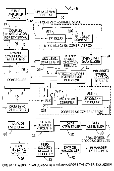
FIGURE 1 shows a digital television signal receiver used for recovering
error-corrected data, which data are suitable for recording by a digital video
cassette
recorder or for MPEG-2 decoding and display in a television set. The FIGURE 1
DTV signal receiver is shown as receiving television broadcast signals from a
receiving antenna 8, but can receive the signals from a cable network instead.
The
13
CA 02220740 1997-11-10
television broadcast signals are supplied as input signal to "front end"
electronics 10.
The "front end" electronics 10 generally include a radio-frequency amplifier
and first
detector for converting radio-frequency television signals to intermediate-
frequency
television signals, supplied as input signal to an intermediate-frequency (I-
F)
amplifier chain 12 for vestigial-sideband DTV signals. The DTV receiver is
preferably of plural-conversion type with the IF amplifier chain 12 including
an
intermediate-frequency amplifier for amplifying DTV signals as converted to an
ultra-high-frequency band by the first detector, a second detector for
converting the
amplified DTV signals to a very-high-frequency band, and a further
intermediate-frequency amplifier for amplifying DTV signals as converted to
the VHF
band. If demodulation to baseband is performed in the digital regime, the IF
amplifier
chain 12 will further include a third detector for converting the amplified
DTV signals
to a final intermediate-frequency band closer to baseband.
Preferably, a surface-acoustic-wave (SAW) filter is used in the IF amplifier
for
the UHF band, to shape channel selection response and reject adjacent
channels. This
SAW filter cuts off rapidly just beyond 5.38 MHz remove from the suppressed
carrier
frequency of the VSB DTV signal and the pilot carrier, which is of like
frequency and
of fixed amplitude. . This SAW filter accordingly rejects much of the
frequency-modulated sound carrier of any co-channel interfering analog TV
signal.
Removing the FM sound carrier of any co-channel interfering analog TV signal
in the
IF amplifier chain 12 prevents artifacts of that carrier being generated when
the final
I-F signal is detected to recover baseband symbols and forestalls such
artifacts
interfering with data-slicing of those baseband symbols during symbol
decoding. The
prevention of such artifacts interfering with data-slicing of those baseband
symbols
during symbol decoding is better than can be accomplished by relying on comb-
filtering before data-slicing.
The final I-F output signals from the IF amplifier chain 12 are supplied to a
complex demodulator 14, which demodulates the vestigial-sideband amplitude-
modulation DTV signal in the final intermediate-frequency band to recover a
real
baseband signal and an imaginary baseband signal. Demodulation may be done in
the
digital regime after analog-to-digital conversion of a final intermediate-
frequency
14
CA 02220740 1997-11-10
band in the few megacycle range as described for example by C. B. Patel et
alii in
U.S. patent No. 5,479,449 issued 26 December 1995 and entitled "DIGITAL VSB
DETECTOR WITH PHASE TRACKER, AS FOR INCLUSION IN AN HDTV
RECEIVER". Alternatively, demodulation may be done in the analog regime, in
which case the results are usually subjected to analog-to-digital conversion
to
facilitate further processing. The complex demodulation is preferably done by
in-phase (I) synchronous demodulation and quadrature-phase (Q) synchronous
demodulation. The digital results of the foregoing demodulation procedures
conventionally have 8-bit accuracy or more and describe 2N-level symbols that
encode N bits of data. Currently, 2N is eight in the case where the FIGURE 1
DTV
signal receiver receives a through-the-air broadcast via the antenna 12 and is
sixteen
in the case where the FIGURE 1 DTV signal receiver receives cablecast. The
concern
of the invention is with the reception of terrestrial through-the-air
broadcasts, and
FIGURE 1 does not show the portions of the DTV receiver providing symbol
decoding and error-correction decoding for received cablecast transmissions. ,
Symbol synchronizer and equalizer circuitry 16 receives at least the digitized
real samples of the in-phase (I-channel) baseband signal from the complex
demodulator 14; in the FIGURE 1 DTV receiver the circuitry 16 is shown also
receiving the digitized imaginary samples of the quadrature-phase (Q-channel)
baseband signal. The circuitry 16 includes a digital filter with adjustable
weighting
coefficients that compensates for ghosts and tilt in the received signal. The
symbol
synchronizer and equalizer circuitry 16 provides symbol synchronization or
"de-rotation" as well as amplitude equalization and ghost removal. Symbol
synchronizer and equalizer circuitry in which symbol synchronization is
accomplished
before amplitude equalization is known from U. S. patent No. x,479,449. In
such
designs the demodulator 14 will supply oversampled demodulator response
containing
real and imaginary baseband signals to the symbol synchronizer and equalizer
circuitry 16. After symbol synchronization, the oversampled data are decimated
to
extract baseband I-channel signal at normal symbol rate, to reduce sample rate
through the digital filtering used for amplitude equalization and ghost
removal.
Symbol synchronizer and equalizer circuitry in which amplitude equalization
precedes
CA 02220740 1997-11-10
symbol synchronization, "de-rotation" or "phase tracking" is also known to
those
skilled in the art of digital signal receiver design.
Each sample of the circuitry 16 output signal is resolved to ten or more bits
and is, in effect, a digital description of an analog symbol exhibiting one of
(2N=8)
levels. The circuitry 16 output signal is carefully gain-controlled by any one
of
several known methods, so the ideal step levels for symbols are known. One
method
of gain control, preferred because the speed of response of such gain control
is
exceptionally rapid, regulates the direct component of the real baseband
signal
supplied from the complex demodulator 14 to a normalized level of +1.25. This
method of gain control is generally described in U. S. patent No. 5,479,449
and is
more specifically described by C. B. Patel et alii in U. S. patent No.
5,573,454 issued
3 June 1997, entitled "AUTOMATIC GAIN CONTROL OF RADIO RECEIVER
FOR RECEIVING DIGITAL HIGH-DEFINITION TELEVISION SIGNALS", and
incorporated herein by reference.
The output signal from the circuitry 16 is supplied as input signal to data
sync
detection circuitry 18, which recovers data field synchronization information
F and
data segment synchronization information S from the equalized baseband I-
channel
signal. Alternatively, the input signal to data sync detection circuitry 18
can be
obtained prior to equalization.
The equalized I-channel signal samples at normal symbol rate supplied as
output signal from the circuitry 16 are applied as the input signal to an
NTSC-rejection comb filter 20. The comb filter 20 includes a first delay
device 201
to generate a pair of differentially delayed streams of the 2N-level symbols
and a first
linear combiner 202 for linearly combining the differentially delayed symbol
streams
2~ to generate the comb filter 20 response, as a first linear combining result
and a
precoding filter response. As described in U. S. patent No. x,260,793, the
first delay
device 201 can provide a delay equal to the period of twelve 2N-level symbols,
and
the first linear combiner 202 can be a subtractor. Each sample of the comb
filter 20
output signal is resolved to ten or more bits and is, in effect, a digital
description of an
analog symbol exhibiting one of (4N-1)=l~ levels.
16
CA 02220740 1997-11-10
The symbol synchronizer and equalizer circuitry 16 is presumed be designed
to suppress the direct bias component of its input signal (as expressed in
digital
samples), which direct bias component has a normalized level of +1.25 and
appears in
the real baseband signal supplied from the complex demodulator 14 owing to
detection of the pilot carrier. Accordingly, each sample of the circuitry 16
output
signal applied as comb filter 20 input signal is, in effect, a digital
description of an
analog symbol exhibiting one of the following normalized levels: -7, -5, -3, -
l, +1, +;,
+5 and +7. These symbol levels are denominated as "odd" symbol levels and are
detected by an odd-level data-dicer 22 to generate interim symbol decoding
results of
000, 001, 010, 011, 100, 101, 110 and 111, respectively.
Each sample of the comb filter 20 output signal is, in effect, a digital
description of an analog symbol exhibiting one of the following normalized
levels:
-14, -12, -10, -8, -6, -4, -2, 0, +2, +4, +6, +8, +10, +12 and +14. These
symbol levels
are denominated as "even" symbol levels and are detected by an even-level data-
slicer
2=~ to generate precoded symbol decoding results of 001, 010, O1 l, 100, 101,
110, 111,
000, 001, 010, O1 l, 100, 101, 110, and 111, respectively. The data-dicers 22
and 24
can be of the so-called "hard decision" type, as presumed up to this point in
the
description, or can be of the so-called "soft decision" type used in
implementing a
Viterbi decoding scheme.
The symbol synchronizer and equalizer circuitry 16 is presumed in the
foregoing description to be designed to suppress the direct bias component of
its input
signal (as expressed in digital samples), which direct bias component has a
normalized level of +1.25 and appears in the real baseband signal supplied
from the
complex demodulator 14 owing to detection of the pilot carrier. Alternatively,
the
symbol synchronizer and equalizer circuitry 16 is designed to preserve the
direct bias
component of its input signal, which simplifies the design of the equalization
filter in
the circuitry 16 somewhat. In such case the data-slicing levels in the odd-
level
data-dicer 22 are offset to take into account the direct bias component
accompanying
the data steps in its input signal. Providing that the first linear combiner
202 is a
subtractor, whether the circuitry 16 is designed to suppress or to preserve
the direct
bias component of its input signal has no consequence in regard to the data-
slicing
17
CA 02220740 1997-11-10
levels in the even-level data-slicer 24. However, if the differential delay
provided by
the first delay device 201 is chosen so that the first linear combiner 202 is
an adder,
the data-slicing levels in the even-level data-slicer 24 should be offset to
take into
account the doubled direct bias component accompanying the data steps in its
input
signal.
A comb filter 26 is used after the data-slicers 22 and 24 to generate a
postcoding filter response to the precoding filter response of the comb filter
20. The
comb filter 26 includes a 3-input multiplexer 261, a second linear combiner
262, and a
second delay device 263 with delay equal to that of the first delay device 201
in the
comb filter 20. The second linear combiner 262 is a modulo-8 adder if the
first linear
combiner 202 is a subtractor and is a modulo-8 subtractor if the first linear
combiner
202 is an adder. The first linear combiner 202 and the second linear combiner
262
may be constructed as respective read-only memories (ROMs) to speed up linear
combination operations sufficiently to support the sample rates involved. The
output
signal from the multiplexer 261 furnishes the response from the postcoding
comb
filter 26 and is delayed by the second delay device 263. The second linear
combiner
262 combines precoded symbol decoding results from the even-level data-slicer
24
with the output signal from the second delay device 263, to generate second
linear
combining results as the output signal of the combiner 262.
The output signal of the multiplexer 261 reproduces one of the three input
signals applied to the multiplexer 261, as selected in response to first,
second and
third states of a multiplexer control signal supplied to the multiplexer 261
from a
controller 28. The first input port of the multiplexer 261 receives ideal
symbol
decoding results supplied from memory within the controller 28 during times
when
2~ data field synchronization information F and data segment synchronization
information S from the equalized baseband I-channel signal are recovered by
the data
sync detection circuitry 18. The controller 28 supplies the first state of the
multiplexer control signal to the multiplexer 261 during these times,
conditioning the
multiplexer 261 to furnish, as the final coding results which are its output
signal, the
ideal symbol decoding results supplied from memory within the controller 28.
The
odd-level data-slicer 22 supplies interim symbol decoding results as its
output signal
18
CA 02220740 1997-11-10
to the second input port of the multiplexes 261. The multiplexes 261 is
conditioned
by the second state of the multiplexes control signal to reproduce the interim
symbol
decoding results, as the final coding results which are its output signal. The
second
linear combines 262 supplies postcoded symbol decoding results as its output
signal to
the third input port of the multiplexes 261. The multiplexes 261 is
conditioned by the
third state of the multiplexes control signal to reproduce the postcoded
symbol
decoding results, as the final coding results which are its output signal.
The postcoding done subsequent to comb filtering and data-slicing has a basic
problem that must be solved in order for the postcoding to operate properly.
One
aspect of this problem is that once error occurs in the partially-filtered
symbol
decoding results, the error is fed back with delay, tending to propagate the
error
during the generation of postcoded symbol decoding results. Other aspects of
this
problem concern how to initialize the conditions in the delayed feedback
circuitry and
how to re-initialize the conditions in the delayed feedback circuitry once
error
propagation occurs. These problems arise when re-coding of the second type is
used
for postcoding because the feedback used in such re-coding is accumulative and
provides a sort of integration over time. When re-coding of the second type is
done
during precoding and re-coding of the first type is done during postcoding,
the re-
coding of the first type provides a sort of differentiation over time that
quickly
suppresses response to the initial conditions of the re-coding of second type.
One
does not have to concern oneself with the initial conditions of accumulation
or
integration. When re-coding of the first type is done during precoding and re-
coding
of the second type is done during postcoding, error caused by incorrect
initial
conditions of accumulation or integration in the re-coding of second type
propagate
themselves during postcoding. The resulting running error in the final
decoding
results is a systematic error, rather than a random error, so generally
speaking the
running error will not be able to self correct itself by chance.
Running errors in the postcoded symbol decoding results from the postcoding
comb filter 26 are curtailed by feeding back the ideal symbol decoding results
supplied from memory within the controller 28 during times data sync detection
circuitry 18 recovers data field synchronization information F and data
segment
19
CA 02220740 1997-11-10
synchronization information S. The generation of these ideal symbol decoding
results
will be described in greater detail further on in this specification. Between
times data
sync detection circuitry 18 recovers data field synchronization information F
and data
segment synchronization information S, by feeding back the best estimates in
the final
symbol decoding result to the second linear combiner 262 via the second delay
device
263, the running errors in the postcoded symbol decoding results from the
postcoding
comb filter 26 can be corrected at times. When the co-channel interfering NTSC
signal has high-luminance white or near-white content, the interim symbol
decoding
result will not be very susceptible to error and will be selected for
supplying the best
estimates in the final symbol decoding result. This corrects running errors.
The output signal from the multiplexer 261 in the postcoding comb filter 26
comprises the final symbol decoding results in 3-parallel-bit groups,
assembled by a
data assembler 30 for application to a data interleaver 32. The data
interleaver 32
commutates the assembled data into parallel data streams for application to
trellis
decoder circuitry 34. Trellis decoder circuitry 34 conventionally uses twelve
trellis
decoders. The trellis decoding results are supplied from the trellis decoder
circuitry
34 to data de-interleaver circuitry 36 for de-commutation. Byte parsing
circuitry 38
converts the data interleaver 36 output signal into bytes of Reed-Solomon
error-correction coding for application to Reed-Solomon decoder circuitry 40,
which
performs Reed-Solomon decoding to generate an error-corrected byte stream
supplied
to a data de-randomizer 42. The data de-randomizer 42 supplies reproduced data
to
the remainder of the receiver (not shown). The remainder of a complete DTV
receiver
will include a packet sorter, an audio decoder, an MPEG-2 decoder and so
forth. The
remainder of a DTV receiver incorporated in a digital tape recorder/reproducer
will
include circuitry for converting the data to a form for recording.
An NTSC co-channel interference detector 44 supplies the controller 28 with
an indication of whether NTSC co-channel interference is of sufficient
strength as to
cause uncorrectable error in the data-slicing performed by the data-slicer 22.
If
detector 44 indicates the NTSC co-channel interference is not of such
strength, the
controller 28 will supply the second state of multiplexer control signal to
the
multiplexer 261 at times other than those times when data field
synchronization
CA 02220740 1997-11-10
information F and data segment synchroriization information S are recovered by
the
data sync detection circuitry 18. This conditions the multiplexer 261 to
reproduce as
its output signal the interim symbol decoding results supplied from the odd-
level
data-dicer 22. If detector 44 indicates the NTSC co-channel interference is of
sufficient strength to cause uncorrectable error in the data-slicing performed
by the
data-slicer 22, the controller 28 will supply the third state of multiplexer
control signal
to the multiplexer 261 at times other than those times when data field
synchronization
information F and data segment synchronization information S are recovered by
the
data sync detection circuitry 18. This conditions the multiplexer 261 to
reproduce as
its output signal the postcoded symbol decoding results provided as second
linear
combining results from the second linear combiner 262.
FIGURE 2 shows a form the NTSC co-channel interference detector 44 can
take, which form is believed to be novel in the art. A subtractor 441
differentially
combines the interim symbol decoding results supplied from the odd-level data-
slicer
1 ~ 22 and the postcoded symbol decoding results provided as second linear
combining
results from the second linear combiner 262. If the amount of NTSC co-channel
interference is negligible, and if the random noise in the baseband I-channel
signal is
negligible, these interim and postcoded symbol decoding results should be
similar, so
the difference output signal from the subtractor 441 should be low. If the
amount of
NTSC co-channel interference is appreciable, however, the difference output
signal
from the subtractor 441 will not be generally low, but rather will often be
high.
A measure of the energy in the difference output signal from the subtractor
441 is developed by squaring the difference output signal with a squarer 442
and
determining the mean average of the squarer response over a prescribed short
time
interval with a mean averaging circuit 443. The squarer 442 can be implemented
using read-only memory (ROM). The mean averaging circuit 443 can be
implemented using a delay line memory for storing several successive digital
samples
and an adder for summing the digital samples currently stored in the delay
line
memory. The short-term mean average of the energy in the difference output
signal
from the subtractor 441, as determined by the mean averaging circuit 443, is
supplied
to a digital comparator connected to provide a threshold detector 444. The
threshold
21
CA 02220740 2001-03-19
in the threshold detector 444 is sufficiently high not to be exceeded the
short-term
mean-average of differences in the random noise accompanying the interim
symbol
decoding results and the postcoded symbol decoding results applied to the
subtractor
441. The threshold is exceeded if the NTSC co-channel interference is of
sufficient
strength as to cause uncorrectable error in the data-slicing performed by the
data-slicer
22. The threshold detector 444 supplies the controller 28 indication of
whether or not
the threshold is exceeded.
FIGURE 3 shows a digital television receiver differing from that of FIGURE I
in that the circuitry for determining whether or not NTSC co-channel
interference is of
sufficient strength as to cause uncorrectable error in the data-slicing
performed by the
data-dicer 22,0
The DTV signal, as converted to
IF by the "front end" electronics 10, is supplied to an IF amplifier chain 46
for NTSC
signals. The IF amplifier chain 46 for NTSC signals differs from the IF
amplifier
chain used in conventional NTSC signal receivers. Insofar as midband gain
characteristics are concerned, amplifier stages in the IF amplifier chain 46
for NTSC
signals correspond to the amplifier stages in the IF amplifier chain 12 for
DTV
signals, having substantially linear gain and having the same automatic gain
control as
the corresponding amplifier stages in the IF amplifier chain 12. The vestigial
sideband
of the NTSC signal is not suppressed in the IF amplifier chain 46. The portion
of the
full sideband of the NTSC signal that is single-sideband in character is
preferably
suppressed in the IF amplifier chain 46 to reduce the energy of co-channel DTV
signal. The reduces the dynamic range of IF amplifier chain =I6 response,
facilitating
additional amplification of video carrier for locking the phase of a local
video carrier
oscillator used in the complex demodulator 48. The filtering procedures to
establish
the bandwidth of the IF amplifier chain 46 can be carried out by SAW filtering
in a
UHF IF amplifier if plural-conversion receiver circuitry is used. The
amplified IF
response of the IF amplifier chain 46 is supplied to a complex demodulator 48
for
NTSC video signal, either directly or after some further amplification. The
complex
22
CA 02220740 2001-03-19
demodulator 48 supplies an in-phase I-channel response composed of samples of
NTSC signal and the real component of accompanying DTV artifacts. The complex
demodulator 48 also supplies a quadrature-phase Q-channel response composed of
samples of the imaginary component of accompanying DTV artifacts, which
samples
are applied to a Hilbert transformation filter ~0. The Hilbert transformation
filter ~0
response is supplied to a linear combiner ~2. The linear combiner ~2 combines
the
Hilbert transformation filter ~0 response with suitably delayed in-phase I-
channel
response, to recover samples of NTSC signal substantially free from
accompanying
DTV artifacts. The linear combiner ~2 is an adder or a subtractor depending on
relative video carrier phasing during the synchronous demodulation procedures
used
in the complex demodulator 48 to generate the I-channel and Q-channel
responses.
The NTSC signal substantially free from accompanying DTV artifacts
supplied from the linear combiner ~2 is applied to a lowpass filter ~4 with a
cut-off
frequency of 750 kHz or less. An estimate of luminance signal energy in the
co-channel interfering NTSC signal is generated by squaring the lowpass filter
~4
response with a squarer ~6 and determining the mean average of the squarer
response
over a prescribed short time interval with a mean averaging circuit ~8. This
estimate
is supplied to a threshold detector ~8. The threshold in the threshold
detector 60 is
exceeded if the NTSC co-channel interference is of sufficient strength as to
cause
uncorrectable error in the data-slicing performed by the data-slicer 22. The
threshold
detector 6u supplies the controller 28 indication of whether or not the
threshold is
exceeded.
FIGURE 4 shows a digital television receiver differing from the FIGURE 1
and FIGURE 3 receivers in that the circuitry for determining whether or not
NTSC
co-channel interference is of sufficient strength as to cause uncorrectable
error in the
data-slicing performed by the data-slicer 22
The DTV signal, as converted to IF by the "front
end" electronics 10, is supplied to an IF amplifier chain 62 of quasi-parallel
type for
NTSC sound signals. The amplifier stages in the IF amplifier chain 62 for NTSC
23
CA 02220740 1997-11-10
sound signals correspond to similar amplifier stages in the IF amplifier chain
12 for
DTV signals, having substantially linear gain and having the same automatic
gain
control as the corresponding amplifier stages in the IF amplifier chain 12.
The
frequency selectivity of the IF amplifier chain 62 is such as to emphasize
response
within ~250 kHz of NTSC audio carrier and within ~250 kHz or so of NTSC video
carrier. The filtering procedures to establish the frequency selectivity of
the IF
amplifier chain 62 can be carried out by SAW filtering in a UHF IF amplifier
if
plural-conversion receiver circuitry is used. The response of the IF amplifier
chain 62
is supplied to an intercarrier detector 64 which uses the modulated NTSC video
carrier as an exalted carrier for heterodyning the NTSC audio carrier to
generate
intercarrier sound intermediate-frequency signal with a 4.5 MHz carrier
frequency.
This intercarrier sound IF signal is amplified by an intercarrier-sound
intermediate-
frequency amplifier 66, which 4.~ MHz IF amplifier 66 supplies amplified
intercarrier
sound IF signal to an intercarrier amplitude detector 68. The response of the
amplitude detector 68 is averaged over a prescribed short time interval with a
mean
averaging circuit 70, and the resulting mean average is supplied to a
threshold detector
72. The threshold in the threshold detector 72 is exceeded if the NTSC co-
channel
interference is of sufficient strength as to cause uncorrectable error in the
data-slicing
performed by the data-dicer 22. The threshold detector 72 supplies the
controller 28
indication of whether or not the threshold is exceeded.
FIGURE 5 shows a preferred way in which the multiplexes 261 in the
postcoding comb filter 26 is implemented. The 3-input multiplexes 261 is shown
as
comprising two 2-input multiplexers 2611 and 2612. The controller 28 applies
the
output signal from the NTSC co-channel interference detector (e. g., 4=l) as
control
2~ signal to the 2-input multiplexes 2611.
If the NTSC co-channel interference is of sufficient strength to cause
uncorrectable error in the data-slicing performed by the data-slices 22, the
resulting
ONE output signal from the NTSC co-channel interference detector conditions
the
multiplexes 2611 to reproduce, for application to the second input port of the
multiplexes 2612, the postcoded symbol decoding results the second linear
combines
262 supplies to the first input port of the multiplexes 2611.
24
CA 02220740 1997-11-10
If the NTSC co-channel interference is of insufficient strength to cause
uncorrectable error in the data-slicing performed by the data-slices 22, the
resulting
ZERO output signal from the NTSC co-channel interference detector conditions
the
multiplexes 2611 to reproduce the interim symbol decoding results the data-
slices 22
supplies to the second input port of the multiplexes 2611. These reproduced
interim
symbol decoding results are applied to the second input port of the
multiplexes 2612.
FIGURES 5, 6 and 7 each show an OR gate 281 being included in the
controller 28. The OR gate 281 supplies a response that is a ONE, when the
field
segment sync detector 181 supplies a ONE thereto in response to the occurrence
of a
field sync segment being detected, and when the data segment sync detector 182
supplies a ONE thereto in response to the occurrence of a data sync code being
detected. At all other times the OR gate 281 supplies a response that is a
ZERO.
In FIGURE 5 the OR gate 281 response is applied as control signal to the
multiplexes 2612. The OR gate 281 response being ZERO conditions the
multiplexes
2612 to reproduce, as final symbol decoding result for application to the data
assembler 30, the output signal of the multiplexes 2611 supplied to the second
input
port of the multiplexes 2612 as better estimate of symbol decoding result. The
OR
gate 281 response being ONE conditions the multiplexes 2612 to reproduce, as
final
symbol decoding result for application to the data assembler, ideal decoding
results
drawn from memory in the controller 28, as will be described in detail further
on in
this specification with reference to FIGURE 8 of the drawing.
FIGURE 6 shows an alternative construction 260 of the post coding comb
filter 26. The 3-input multiplexes 261 comprising two 2-input multiplexers
2611 and
2612 is replaced by a 3-input multiplexes 2610 comprising three 2-input
multiplexers
26101, 26102 and 26103.
FIGURE 7 shows a modification 2600 of the post coding comb filter 26, in
which the 3-input multiplexes 261 comprising two 2-input multiplexers 2611 and
2612 is replaced by a 3-input multiplexes 26100 comprising two 2-input
multiplexers
261001 and 261002 receiving their respective control signals from the OR gate
281
and from the NTSC co-channel interference detector. The post coding comb
filter
CA 02220740 1997-11-10
2600 provides somewhat different operating result than the post coding comb
filters
26 and 260. The multiplexer 261001 replaces postcoded symbol decoding results
with ideal symbol decoding results when the OR gate 281 response is ONE. When
NTSC co-channel interference detector supplies a ONE indicative that NTSC
co-channel interference is of sufficient strength to cause uncorrectable error
in the
data-slicing performed by the data-dicer 22, a multiplexer 261002 selects the
resulting
modified postcoded symbol decoding results as final symbol decoding results
for
application to the data assembler 30. When NTSC co-channel interference
detector
supplies a ZERO indicative that NTSC co-channel interference is of
insufficient
strength to cause uncorrectable error in the data-slicing performed by the
data-dicer
22, the multiplexer 261002 selects the interim symbol decoding results from
the
data-slicer 22 as final symbol decoding results for application to the data
assembler
30, without any replacement of those interim symbol decoding results by ideal
symbol
decoding results.
FIGURE 8 shows the multiplexer 2612 of FIGURE 5 in greater detail,
together with the circuitry for generating the ideal symbol decoding results
applied to
the multiplexer 2612. The multiplexer 2612 comprises the output buffer
registers of
read-only memories (ROMs) 74, 76, 78 for selectively reading to a 3-bit-wide
output
bus 80 from the multiplexer 2612. The multiplexer 2612 further comprises a tm-
state
buffer 82 for selectively forwarding the 3-bit-wide output of the multiplexer
2611 to
the output bus 80.
The circuitry for generating the ideal symbol decoding results applied to the
multiplexer 2612 comprises the ROMs 74, 76, 78; a symbol clock generator 84;
an
address counter 86 for addressing the ROivIs 74, 76, 78; jam reset circuitry
88 for
resetting the counter 86; the address decoders 94, 96, 98 for generating read
enable
signals for the ROMs 74, 76, 78; and a NOR gate 92 for controlling the tri-
state buffer
82. The address counter 86 counts input pulses received at symbol decoding
rate from
the symbol clock generator 84, thereby to generate successive addresses
respectively
descriptive of the symbols in one data frame. Suitable portions of these
addresses are
applied to the ROMs 74, 76, 78 as their input addresses. The jam reset
circuitry 88
resets the counter 86 to appropriate counts responsive to data field
synchronization
26
CA 02220740 1997-11-10
information F and data segment synchronization information S recovered by the
data
sync detection circuitry 18 of FIGURE 1, 3 or 4.
It is preferable to configure the counter 86 so a group of more significant
bits
counts the number of data segments per data frame and so a group of less
significant
bits counts the number of symbols per data segment. This simplifies the design
of the
jam reset circuitry 88; reduces the bit-widths of input signal to the address
decoders
94, 96, 98; and facilitates the ROMs 74, 76, 78 being addressed by partial
addresses
from the counter 86, reducing the bit widths of ROM addressing.
The ROM 74 stores ideal symbol decoding results for an odd field sync
segment and is selectively enabled for reading by receiving a ONE from the
address
decoder 94. The ROM 74 is addressed by the group of less significant bits of
counter
86 output that counts the number of symbols per data segment group; and the
address
decoder 94 responds to the group of more significant bits that counts the
number of
data segments per data frame. The address decoder 94 generates a ONE when.and
only when the data segment portion of the address supplied by the address
counter 86
corresponds to the address of an odd field sync segment.
The ROM 76 stores ideal symbol decoding results for an even field sync
segment and is selectively enabled for reading by receiving a ONE from the
address
decoder 96. The ROM 76 is addressed by the group of less significant bits of
counter
86 output that counts the number of symbols per data segment group; and the
address
decoder 96 responds to the group of more significant bits that counts the
number of
data segments per data frame. The address decoder 96 generates a ONE when and
only when the data segment portion of the address supplied by the address
counter 86
corresponds to the address of an even field sync segment.
The ROM 78 stores ideal symbol decoding results for the start code group at
the beginning of each sync segment and is selectively enabled for reading by
receiving
a ONE from the address decoder 98. The ROM 78 responds to the two least
significant bits of counter 86 output; and the address decoder 98 responds to
the group
of less significant bits of counter 86 output that counts the number of
symbols per data
segment group. The address decoder 98 generates a ONE when and only when the
27
CA 02220740 1997-11-10
data symbol per data segment count portion of the address supplied by the
address
counter 86 corresponds to the partial address of a start code group.
The NOR gate 92 receives the responses of the address decoders 94, 96 and 98
at respective ones of its three input connections. When ideal symbol decoding
results
are available, one of the address decoders 94, 96 and 98 supplies a ONE as its
output
signal, conditioning the NOR gate 92 to supply a ZERO response to the tri-
state data
buffer 82. This conditions the tri-state data buffer 82 to exhibit a high
source
impedance to the data bus 80, so the signal forwarded from the multiplexer
2611 will
not be asserted on the 3-bit-wide data bus 80 from the multiplexer 2612.
During those
portions of data segments for which ideal symbol decoding results are not
predictable,
none of the address decoders 94, 96 and 98 supplies a ONE as its output
signal,
conditioning the NOR gate 92 to supply a ONE response to the tri-state data
buffer 82.
This conditions the tri-state data buffer 82 to exhibit a low source impedance
to the
data bus 80, so the signal forwarded from the multiplexer 2611 will be
asserted on the
3-bit-wide data bus 80 from the multiplexer 2612.
The FIGURE 8 circuitry for generating ideal symbol decoding results applied
to the multiplexer 2612 is readily adapted by one skilled in the art of
digital circuit
design for use in the configurations shown in FIGURES 6 and 7.
FIGURE 9 is a block schematic diagram showing details of a portion of the
FIGURE 1, FIGURE 3 or FIGURE 4 digital television signal receiver using a
species
120 of the NTSC-rejection comb filter 20 and a species 126 of the postcoding
comb
filter 26. A subtractor 1202 serves as the first linear combiner in the NTSC-
rejection
comb filter 120, and a modulo-8 adder 1262 serves as the second linear
combiner in
the postcoding comb filter 126. The NTSC-rejection comb filter 120 uses a
first delay
device 1201 exhibiting a delay of twelve symbol epochs, and the postcoding
comb
filter 126 uses a second delay device 1263 also exhibiting a delay of twelve
symbol
epochs. The 12-symbol delay exhibited by each of the delay devices 1201 and
1263 is
close to one cycle delay of the artifact of the analog TV video carrier at
59.75 times
the analog TV horizontal scan frequency fH. The 12-symbol delay is close to
five
cycles of the artifact of the analog TV chrominance subcarrier at 287.25 times
fH. The
28
CA 02220740 1997-11-10
12-symbol delay is close to six cycles of the artifact of the analog TV sound
carrier at
345.75 times fH. This is the reason that the differentially combined response
of the
subtractor 1202 to the audio carrier, to the video carrier and to frequencies
close to
chrominance subcarrier differentially delayed by the first delay device 1201
tends to
have reduced co-channel interference. However, in portions of a video signal
in
which edges cross a horizontal scan line, the amount of correlation in the
analog TV
video signal at such distances in the horizontal spatial direction is quite
low.
A species 1261 of the multiplexer 261 is controlled by a multiplexer control
signal that is in its second state most of the time when it is determined
there is
insufficient NTSC co-channel interference to cause uncorrectable error in the
output
signal from the data-slicer 22 and that is in its third state most of the time
when it is
determined there is sufficient NTSC co-channel interference to cause
uncorrectable
error in the output signal from the data-slicer 22. The multiplexer 1261 is
conditioned
by its control signal being in its third state to feed back the modulo-8 sum
results of
the adder 1262, as delayed twelve symbol epochs by the delay device 1263, to~
the
adder 1262 as a summand. This is a modular accumulation procedure in which a
single error propagates as a running error, with error recurring every twelve
symbol
epochs. Running errors in the postcoded symbol decoding results from the
postcoding
comb filter 126 are curtailed by the multiplexer 1261 being placed into its
first state
for four symbol epochs at the beginning of each data segment, as well as
during the
entirety of each data segment containing field sync. When this control signal
is in its
first state, the multiplexer 1261 reproduces as its output signal ideal symbol
decoding
results supplied from memory in the controller 28. The introduction of ideal
symbol
decoding results into the multiplexer 1261 output signal halts a running
error. Since
there are 4 + 69(12) symbols per data segment, the ideal symbol decoding
results slip
back four symbol epochs in phase each data segment, so no running error can
persist
for longer than three data segments.
FIGURE 10 is a block schematic diagram showing details of a portion of the
FIGURE 1, FIGURE 3 or FIGURE 4 digital television signal receiver using a
species
220 of the NTSC-rejection comb filter 20 and a species 226 of the postcoding
comb
filter 26. The NTSC-rejection comb filter 220 uses a first delay device 2201
29
CA 02220740 2001-03-19
exhibiting a delay of six symbol epochs, and the postcoding comb filter 226
uses a
second delay device 2263 also exhibiting a delay of six symbol epochs. The 6-
symbol
delay exhibited by each of the delay devices 2201 and 2263 is close to 0.5
cycle delay
of the artifact of the analog TV video carrier at 59.75 times the analog TV
horizontal
scan frequency fH, close to 2.5 cycles of the artifact of the analog TV
chrominance
subcarrier at 287.25 times fH, and close to 3 cycles of any artifact of the
analog TV
audio carrier at 345.75 times fH. An adder 2202 serves as the first linear
combines in
the NTSC-rejection comb filter 220, and a modulo-8 subtractor 2262 serves as
the
second linear combines in the postcoding comb filter 226. Since the delay
exhibited
by the delay devices 2201 and 2263 is shorter than the delay exhibited by the
delay
devices 1201 and 1263, although nulls near frequencies converted from analog
TV
carrier frequencies are narrower band, there is more likely to be good anti-
correlation
in the signals additively combined by the adder 2202 than there is likely to
be good
correlation in the signals differentially combined by the subtractor 1202. The
1 S suppression of the sound carrier is poorer in the N'TSC-rejection comb
filter 220
response than in the NTSC-rejection comb filter 120 response. However, if the
sound
carrier of a co-channel interfering analog TV signal has been suppressed by
SAW
filtering or a sound trap in the IF amplifier chain 12, the poor sound
rejection of the
comb filter 220 is not a problem. The responses to sync tips is reduced in
duration .
using the NTSC-rejection comb filter 220 of FIGURE 10 rather than the
NTSC-rejection comb filter 120 of FIGURE 9, so there is substantially reduced
tendency to overwhelm error-correction in the trellis decoding and Reed-
Solomon
coding.
A species 2261 of the multiplexes 261 is controlled by a multiplexes control
signal that is in its second state most of the time when it is determined
there is
insufficient NTSC co-channel interference to cause uncorrectable error in the
output
signal from the data-slices 22 and that is in its third state most of the time
when it is
determined there is sufficient NTSC co-channel interference to cause
uncorrectable
error in the output signal from the data-slices 22. The multiplexes 2261 is
conditioned
by its control signal being in its third state to feed back the modulo-8 sum
results of
the adder Z20Zas delayed six symbol epochs by the delay device 2263, to the
adder
CA 02220740 2001-03-19
2 2 0 2 as a summand. This is a modular accumulation procedure in which a
single error
propagates as a running error, with error recurring every six symbol epochs.
Running
errors in the postcoded symbol decoding results from the postcoding comb
filter 226
are curtailed by the multiplexes 2261 being placed into its first state for
four symbol
epochs at the beginning of each data segment, as well as during the entirety
of each
data segment containing field sync. When this control signal is in its first
state, the
multiplexes 2261 reproduces as its output signal ideal symbol decoding results
supplied from memory in the controller 28. The introduction of ideal symbol
decoding results into the multiplexes 2261 output signal halts a running
error. Since
there are 4 + 138(6) symbols per data segment, the ideal symbol decoding
results slip
back four symbol epochs in phase each data segment, so no running error can
persist
.,
for longer than two data segments. The likelihood of a protracted period of
running
error in the postcoding comb filter 226 is substantially less than in the
postcoding
comb filter 126, although the running error recurs more frequently and affects
twice as
many of the twelve interleaved trellis codes.
,,
' FIGURE 11 is a block schematic diagram showing details of a portion of the
FIGURE 1, FIGURE 3 or FIGURE 4 digital television signal receiver using a
species
320 of the NTSC-rejection comb filter 20 and a species 326 of the postcoding
comb
filter 26. The NTSC-rejection comb filter 320 uses a first delay device 3201
exhibiting a delay of 1368 symbol epochs, which delay is substantially equal
to the
epoch of two horizontal scan lines of an analog TV signal, and the postcoding
comb
filter 326 uses a second delay device 3263 also exhibiting such delay. The
first linear
combines in the NTSC-rejection comb filter 320 is a: subtractor 3202, and the
second
linear combines in the postcoding comb filter 326 is a modulo-8 adder 3262
A species 3261 of the multiplexes 261 is controlled by a multiplexes control
signal that is in its second state most of the time when it is determined
there is
insufficient NTSC co-channel interference to cause uncorrectable error in the
output
signal from the data-slices 22 and that is in its third state most of the time
when it is
determined there is sufficient NTSC co-channel interference to cause
uncorrectable
error in the output signal from the data-slices 22. The DTV receiver
preferably
contains circuitry for detecting change between alternate scan lines in the
NTSC
31
CA 02220740 1997-11-10
co-channel interference, so that the controller 28 can withhold supplying the
third
state of the multiplexer 3261 control signal under such conditions.
The multiplexer 3261 is conditioned by its control signal being in its third
state to feed back the modulo-8 sum results of the adder 3262, as delayed 1368
symbol epochs by the delay device 3263, to the adder 3262 as a summand. This
is a
modular accumulation procedure in which a single error propagates as a running
error,
with error recurring every 1368 symbol epochs. This symbol code span is longer
than
the span for a single block of the Reed-Solomon code, so a single running
error is
readily corrected during Reed-Solomon decoding. Running errors in the
postcoded
symbol decoding results from the postcoding comb filter 326 are curtailed by
the
multiplexer 3261 being placed into its first state during the entirety of each
data
segment containing field sync, as well as for four symbol epochs at the
beginning of
each data segment. When this control signal is in its first state, the
multiplexer 3261
reproduces as its output signal ideal symbol decoding results supplied from
memory
in the controller 28. The introduction of ideal symbol decoding results into
the
multiplexer 3261 output signal halts a running error. The 16.67 millisecond
duration
of an NTSC video field exhibits phase slippage against the 24.19 millisecond
duration
of a DTV data field, so the DTV data segments containing field sync eventually
scan
the entire NTSC frame raster. The 525 lines in the NTSC frame raster each
contain
684 symbol epochs, for a total of 359,100 symbol epochs. Since this is
somewhat less
than 432 times the 832 symbol epochs in a DTV data segment containing field
sync,
one can guess with reasonable confidence that running errors of duration
longer than
432 data fields will be expunged by the multiplexer 3261 reproducing ideal
symbol
decoding results during DTV data segments containing field sync. There is also
phase
slippage between data segments, for the start code groups of which ideal
symbol
decoding results are available, and NTSC video scan lines. One can estimate
39,100
symbol epochs, which is 89,775 times the four symbol epochs in a code start
group,
are scanned during 89,77 consecutive data segments. Since there are 313 data
segments per DTV data field, one can guess with reasonable confidence that
running
errors of duration longer than 287 data fields will be expunged by the
multiplexer
3261 reproducing ideal symbol decoding results during the code start groups.
The
32
CA 02220740 1998-06-25
two sources of suppression of running errors are reasonably independent of
each
other, so running errors of duration longer than two hundred or so data fields
are quite
unlikely. Furthermore, if NTSC co-channel interference dips low at a time when
the
running error recurs, to condition the multiplexer 3261 for reproducing the
response
of the data-slicer 22 as its output signal, the error may be corrected earlier
than would
otherwise be the case.
The FIGURE 11 NTSC-rejection comb filter 320 is quite good in suppressing
demodulation artifacts generated in response to analog TV horizontal
synchronizing
pulses, as well as suppressing many of the demodulation artifacts generated in
response to analog TV vertical synchronizing pulses and equalizing pulses.
These
artifacts are the co-channel interference with highest energy. Except where
there is
scan-line-to-scan-line change in the video content of the analog TV signal
over the
period of two scan lines, the NTSC-rejection comb filter 320 provides
reasonably
good suppression of that video content regardless of its color. The
suppression of the
FM audio carrier of the analog TV signal is reasonably good, in case it has
not been
suppressed by~a tracking rejection filter in the symbol synchronization and
equalization circuitry 16. Artifacts of most analog TV color bursts are
suppressed in
the NTSC-rejection comb filter 320 response, too. Furthermore, the filtering
provided
by the NTSC-rejection comb filter 320 is "orthogonal" to the NTSC-interference
rejection built into the trellis decoding procedures.
FIGURE 12 is a block schematic diagram showing details of a portion of the
FIGURE l, FIGURE 3 or FIGURE 4 digital television signal receiver using a
species
420 of the NTSC-rejection comb filter 20 and a species 426 of the postcoding
comb
filter 26. The NTSC-rejection comb filter 420 uses a first delay device 4201
exhibiting a delay of 179,208 symbol epochs, which delay is substantially
equal to the .
period of 262 horizontal scanning lines of an analog TV signal, and the
postcoding
comb filter 426 uses a second delay device 4261 also exhibiting such delay. A
subtractor
4202 serves as the first linear combiner in the NTSC-rejection comb filter
420, and a
modulo-8 adder ' 4262 serves as the second linear combiner in the postcoding
comb filter 426.
33
CA 02220740 1997-11-10
A species 4261 of the multiplexer~261 is controlled by a multiplexes control
signal that is in its second state most of the time when it is determined
there is
insufficient NTSC co-channel interference to cause uncorrectable error in the
output
signal from the data-dicer 22 and that is in its third state most of the time
when it is
determined there is sufficient NTSC co-channel interference to cause
uncorrectable
error in the output signal from the data-slices 22. The DTV receiver
preferably
contains circuitry for detecting field-to-field change in the NTSC co-channel
interference, so that the controller 28 can withhold supplying the third state
of the
multiplexes 4261 control signal under such conditions.
The multiplexes 4261 is conditioned by its control signal being in its third
state to feed back the modulo-8 sum results of the adder 4262, as delayed
179,208
symbol epochs by the delay device 4263, to the adder 4262 as a summand. This
is a
modular accumulation procedure in which a single error propagates as a running
error,
with error recurring every 179,208 symbol epochs. This symbol code span is
longer
than the span for a single block of the Reed-Solomon code, so a single running
error is
readily corrected during Reed-Solomon decoding. Running errors in the
postcoded
symbol decoding results from the postcoding comb filter 426 are curtailed by
the
multiplexes 4261 being placed into its first state during the entirety of each
data
segment containing field sync, as well as for four symbol epochs at the
beginning of
each data segment. When this control signal is in its first state, the
multiplexes 4261
reproduces as its output signal ideal symbol decoding results supplied from
memory
in the controller 28. The introduction of ideal symbol decoding results into
the
multiplexes 4261 output signal halts a running error. The maximum number of
data
fields required to expunge running error in the multiplexes 4261 output signal
is
2~ presumably substantially the same as required to expunge running error in
the
multiplexes 3261 output signal. However, the number of times the error recurs
in that
period is lower by a factor of 131.
The FIGURE 12 NTSC-rejection comb filter 420 suppresses most
demodulation artifacts generated in response to analog TV vertical
synchronizing
pulses and equalizing pulses, as well as suppressing all the demodulation
artifacts
generated in response to analog TV horizontal synchronizing pulses. These
artifacts
34
CA 02220740 1997-11-10
are the co-channel interference with highest energy. Also, the NTSC-rejection
comb
filter 420 suppresses artifacts arising from the video content of the analog
TV signal
that does not change from field to field or line-to-line, getting rid of
stationary
patterns irrespective of their horizontal spatial frequency or color.
Artifacts of most
analog TV color bursts are suppressed in the NTSC-rejection comb filter 420
response, too
FIGURE 13 is a block schematic diagram showing details of a portion of the
FIGURE 1, FIGURE 3 or FIGURE 4 digital television signal receiver using a
species
520 of the NTSC-rejection comb filter 20 and a species 526 of the postcoding
comb
filter 26. The NTSC-rejection comb filter 520 uses a first delay device 5201
exhibiting a delay of 718,200 symbol epochs, which delay is substantially
equal to
the period of two frames of an analog TV signal, and the postcoding comb
filter 526
uses a second delay device 5261 also exhibiting such delay. A subtractor 5202
serves
as the first linear combines in the NTSC-rejection comb filter 520, and a
modulo-8
1 ~ adder 5262 serves as the second linear combines in the postcoding comb
filter'S26.
A species 5261 of the multiplexes 261 is controlled by a multiplexes control
signal that is in its second state most of the time when it is determined
there is
insufficient NTSC co-channel interference to cause uncorrectable error in the
output
signal from the data-dicer 22 and that is in its third state most of the time
when it is
determined there is sufficient NTSC co-channel interference to cause
uncorrectable
error in the output signal from the data-dicer 22. The DTV receiver preferably
contains circuitry for detecting change between alternate frames in the NTSC
co-channel interference, so that the controller 28 can withhold supplying the
third
state of the multiplexes 5261 control signal under such conditions.
The multiplexes 5261 is conditioned by its control signal being in its third
state to feed back the modulo-8 sum results of the adder 5262, as delayed
718,200
symbol epochs by the delay device 5263, to the adder 5262 as a summand. This
is a
modular accumulation procedure in which a single error propagates as a running
error,
with error recurring every 718,200 symbol epochs. This symbol code span is
longer
than the span for a single block of the Reed-Solomon code, so a single running
error is
CA 02220740 1997-11-10
readily corrected during Reed-Solomon decoding. Running errors in the
postcoded
symbol decoding results from the postcoding comb filter 526 are curtailed by
the
multiplexer 5261 being placed into its first state during the entirety of each
data
segment containing field sync, as well as for four symbol epochs at the
beginning of
each data segment. When this control signal is in its first state, the
multiplexer X261
reproduces as its output signal ideal symbol decoding results supplied from
memory
in the controller 28. The introduction of ideal symbol decoding results into
the
multiplexes X261 output signal halts a running error. The maximum number of
data
fields required to expunge running error in the multiplexes X261 output signal
is
presumably substantially the same as required to expunge running error in the
multiplexes 3261 output signal. However, the number of times the error recurs
in that
period is lower by a factor of 525.
The FIGURE 13 NTSC-rejection comb filter X20 suppresses all demodulation
artifacts generated in response to analog TV vertical synchronizing pulses and
equalizing pulses, as well as suppressing all the demodulation artifacts
generated in
response to analog TV horizontal synchronizing pulses. These artifacts are the
co-
channel interference with highest energy. Also, the NTSC-rejection comb filter
X20
suppresses artifacts arising from the video content of the analog TV signal
that does
not change over two frames, getting rid of such very stationary patterns
irrespective of
their spatial frequency or color. Artifacts of all analog TV color bursts are
suppressed
in the NTSC-rejection comb filter X20 response, too.
One skilled in the art of television system design will discern other
properties
of correlation and anti-correlation in analog TV signals that can be exploited
in the
design of NTSC-rejection filters of still other types than those shown in
FIGURES 9 -
2~ 13. The use of NTSC-rejection filters that cascade two NTSC-rejection
filters of the
types already disclosed increases the 2N levels of the baseband signals to (8N-
1) data
levels. Such filters may be required to overcome particularly bad co-channel
interference problems despite their shortcoming of reducing signal-to-noise
for
random noise interference with symbol decoding.
36
CA 02220740 1997-11-10
FIGURE 14 shows a modification of a digital television signal receiver as
thusfar described, constructed in accordance with a further aspect of the
invention so
as to operate in parallel a plurality of symbol decoders using respective even-
level
data-slicers, each preceded by a different type of NTSC-rejection comb filter
and each
succeeded by a respective postcoding comb filter to compensate for the
precoding
introduced by the preceding NTSC-rejection comb filter. An even-level data-
slicer
A24 converts the response of an NTSC-rejection filter A20 of a first type to
first
precoded symbol decoding results for application to a postcoding comb filter
A26 of a
first type. An even-level data-slicer B24 converts the response of an NTSC-
rejection
filter B20 of a second type to second precoded symbol decoding results for
application to a postcoding comb filter B26 of a second type. An even-level
data-slicer C24 converts the response of an NTSC-rejection filter C20 of a
third type
to third precoded symbol decoding results for application to a postcoding comb
filter
C26 of a third type. The odd-level data-slicer 22 supplies interim symbol
decoding
results to the postcoding comb filters A26, B26 and C26. The prefixes A, B and
C in
the identification numbers for the elements of FIGURE 14 are different
integers which
will correspond to respective ones of the integers 1, 2, 3, 4 and 5 when
receiver
portions as shown in ones of FIGURES 9-13 are employed.
Symbol decoding selection circuitry 90 in FIGURE 14 formulates a best
estimate of correct symbol decoding for application to the trellis decoding
circuitry
34, selecting from the interim symbol decoding results received from the data-
slicer
22 and the various postcoded symbol coding results received from postcoding
comb
filters A26, B26 and C26. The best estimate of symbol decoding results are
used to
correct the summation procedures in the postcoding comb filters A26, B26 and
C26.
FIGURE 1 ~, comprising FIGURES 1 ~A and 1 ~B, illustrates in greater detail a
currently preferred way of implementing the symbol decoding selection
circuitry 90.
FIGURE 15A shows details of circuitry for generating prescribed symbol
decoding
results for application, during data synchronization intervals, to the 3-bit-
wide output
data bus 800 of the symbol decoding selection circuitry 90. The 1 SA circuitry
operates similarly to circuitry described above with reference to FIGURE 8.
37
CA 02220740 1997-11-10
FIGURE 15B illustrates in greater detail circuitry within the symbol decoding
selection circuitry 90 for selecting among the interim symbol decoding results
and the
various postcoded symbol decoding results, for generating final symbol
decoding
results during time periods between data synchronization intervals. The
efficacies of
the NTSC-rejection filters A20, B20 and C20 in removing NTSC co-channel
interference from DTV signal are determined by observing how well related
NTSC-rejection filters A100, B100 and C100 reduce the energy of NTSC co-
channel
interference translated to baseband and separated from DTV signal artifacts.
Separation of NTSC co-channel interference from DTV signal proceeds as
previously
described with reference to FIGURE 3. The lowpass filter ~4 response to
baseband
video that has been synchronously detected from the NTSC co-channel
interference is
supplied as input signal to NTSC-rejection filters A100, B100 and C100. The
NTSC-
rejection filter A100 differs from the NTSC-rejection filter A20 of first type
insofar as
the type of linear combiner that is used, the linear combiner in one of the
filters A20
and A100 being an adder and the linear combiner in the other of the filters
A20 and
A100 being a subtractor. This is because the filter A100 is supplied baseband
video,
but the artifact of NTSC video carrier in the DTV signal supplied to the
filter A20 is
not at baseband for video carrier. For similar reasons, the NTSC-rejection
filter B100
differs from the NTSC-rejection filter B20 of second type insofar as the type
of linear
combiner that is used, and the NTSC-rejection filter C100 differs from the
NTSC-rejection filter C20 of third type insofar as the type of linear combiner
that is
used. The responses of the NTSC-rejection filters A100, B100 and C100 are
squared
by squarers A102, B102 and C102, respectively, for determining the energies of
these
responses. The response of the lowpass filter ~4 is squared by a squarer 104
for
determining its energy.
FIGURE 15B modifies the FIGURE 8 circuitry to replace the multiple~er
2611 and the tri-state data buffer 82 with four tri-state data buffers 082,
A82, B82 and
C82. The tri-state data buffer 082 is used for selectively asserting the
interim symbol
decoding results from the data-slicer 22 onto the 3-bit-wide output data bus
800 of the
symbol decoding selection circuitry 90. The three tri-state data buffers A82,
B82 and
38
CA 02220740 1997-11-10
C82 are used for selectively asserting the postcoded symbol decoding results
from the
postcoding comb filters A26, B26 and C26, respectively, onto the data bus 800.
It is to be determined whether any of the responses of the NTSC-rejection
filters A100, B100 and C100 has substantially less energy than the response of
the
lowpass filter ~4 to determine that one of the three tri-state data buffers
A82, B82 and
C82, rather than the tri-state data buffer 082, is to be conditioned for
providing low
source impedance when the NOR gate 92 response is ONE. If such determination
is
made it is to be further determined which of the responses of the NTSC-
rejection
filters A100, B100 and C100 has the least remaining energy therein, to govern
which
of the three tri-state data buffers 082, A82, B82 and C82 is to be conditioned
for
providing low source impedance when the NOR gate 92 response is ONE. Towards
these goals, the responses of squarers 104 and A102 are compared by a
comparator
106; the responses of squarers 104 and B102 are compared by a comparator 108;
the
responses of squarers 104 and C102 are compared by a comparator 110; the
responses
of squarers A102 and B102 are compared by a comparator 112; the responses bf
squarers A102 and C102 are compared by a comparator 114; and the responses of
squarers B102 and C102 are compared by a comparator 112.
A 3-input NOR gate 118 responds to none of the comparators 106, 108 and
110 indicating that the response of squarer 104 exceeds any of the responses
of the
squarers A102, B102 and C102 to furnish a ONE as output signal; otherwise the
NOR
gate 118 output signal is a ZERO. A 2-input AND gate 120 supplies a ONE
response
that conditions the three tri-state data buffer 082 for providing low source
impedance
when and only when NOR gate 92 response is ONE at the same time that the NOR
gate 118 response is a ONE.
A 3-input AND gate 122 furnishes a ONE output signal responsive to the
output of the comparator 106 being a ONE, indicative that the squarer A102
response
has less energy than the squarer 104 response, at the same time both of the
complemented outputs of the comparators 112 and 114 are ONES, indicative that
the
response of squarer 104 has no more energy than the responses of the squarers
B102
and C102; otherwise the AND gate 122 output signal is a ZERO. A 2-input AND
39
CA 02220740 1997-11-10
gate 124 supplies a ONE response that conditions the three tri-state data
buffer A82
for providing low source impedance when and only when NOR gate 92 response is
ONE at the same time that the AND gate 122 response is a ONE.
A 3-input AND gate 126 furnishes a ONE output signal responsive to the
complemented output of the comparator 116 being a ONE, indicative that the
squarer
B102 response has no more energy than the squarer C102 response, at the same
both
of the outputs of the comparators 108 and 112 are ONES, indicative that the
response
of squarer B102 has less energy than the responses of the squarers 104 and
A102;
otherwise the AND gate 126 output signal is a ZERO. A 2-input AND gate 128
supplies a ONE response that conditions the three tri-state data buffer B82
for
providing low source impedance when and only when NOR gate 92 response is ONE
at the same time that the AND gate 126 response is a ONE.
A 3-input AND gate 130 furnishes a ONE output signal when the outputs of
the comparators 110, 114 and 116 are all ONES, indicative that the response of
squarer C102 has less energy than the responses of the squarers 104, A102 and
B102;
otherwise the AND gate 130 output signal is a ZERO. A 2-input AND gate 132
supplies a ONE response that conditions the three tri-state data buffer C82
for
providing low source impedance when and only when NOR gate 92 response is ONE
at the same time that the AND gate 130 response is a ONE.
Referring back to FIGURE 14, the NTSC-rejection comb filter A20 and the
postcoding comb filter A26 circuitry are advantageously chosen to be of types
like the
NTSC-rejection comb filter X20 and the postcoding comb filter X26 circuitry of
FIGURE 13. This is so despite a considerable cost in memory, since 718,200
symbols
have to be stored in each of the 2-video-frame delays X201 and X263. (However,
the
2~ storage in the 2-video-frame delay X201 provides the storage required for
the FIGURE
15 co-channel interference detector A44. Furthermore, the same memory can be
used
for realizing the shorter delays 4201, 3201, 2201, 1201 and the shorter delays
in the
other co-channel interference detectors of FIGURE 15. Also, the storage in the
2-
video-frame delay X263 provides the storage required for shorter delays 4263,
3263,
2263, 1263.)
CA 02220740 1997-11-10
The high-energy demodulation artifacts generated in response to analog TV
synchronizing pulses, equalizing pulses, and color bursts are all suppressed
when the
NTSC-rejection comb filter A20 additively combines alternate video frames.
Also,
artifacts arising from the video content of the analog TV signal that does not
change
over two frames are suppressed, getting rid of stationary patterns
irrespective of their
spatial frequency or color. When NTSC-rejection comb filter A20 additively
combines alternate video frames, the NTSC-rejection comb filter A100
differentially
combines those alternate video frames and together with the squarer A102
provides a
detector for change between alternate frames in the NTSC co-channel
interference.
The remaining problem of suppressing demodulation artifacts primarily
concerns suppressing those demodulation artifacts arising from frame-to-frame
difference at certain pixel locations within the analog TV signal raster.
These
demodulation artifacts can be suppressed by intra-frame filtering techniques.
The
NTSC-rejection comb filter B20 and the postcoding comb filter B26 circuitry
can be
1 ~ chosen to suppress remnant demodulation artifacts by relying on
correlation in the
horizontal direction, and the NTSC-rejection comb filter C20 and the
postcoding
comb filter C26 circuitry can be chosen to suppress remnant demodulation
artifacts by
relying on correlation in the vertical direction. Consider how such a design
decision
can be further implemented.
If the sound carrier of a co-channel interfering analog TV signal is not
suppressed by SAW filtering or a sound trap in the IF amplifier chain 12, the
NTSC-rejection comb filter B20 and the postcoding comb filter B26 circuitry
are
advantageously chosen to be of types like the NTSC-rejection comb filter 120
and the
postcoding comb filter 126 circuitry of FIGURE 9. If the sound carrier of a co-
2~ channel interfering analog TV signal is suppressed by SAW filtering or a
sound trap
in the IF amplifier chain 12, the NTSC-rejection comb filter B20 and the
postcoding
comb filter B26 circuitry are advantageously chosen to be of types like the
NTSC-
rejection comb filter 220 and the postcoding comb filter 226 circuitry of
FIGURE 10.
This is because the anti-correlation between video components only six symbol
epochs away from each other is usually better than the correlation between
video
components twelve symbol epochs away from each other.
41
CA 02220740 1997-11-10
The optimal choice of the NTSC-rejection comb filter C20 and the postcoding
comb filter C26 circuitry is less straightforward, because of the choice one
must make
(in consideration of field interlace in the interfering analog TV signal)
whether to
choose the temporally closer scan line in the same field or the spatially
closer line in
the preceding field to be combined with the current scan line in the NTSC-
rejection
comb filter C20. Choosing the temporally closer scan line in the same field is
generally the better choice, since jump cuts between fields are less likely to
ravage
NTSC rejection by the comb filter C20. With such choice, the NTSC-rejection
comb
filter C20 and the postcoding comb filter C26 circuitry are of types like the
NTSC-
rejection comb filter 320 and the postcoding comb filter 326 circuitry of
FIGURE 11.
When NTSC-rejection comb filter C20 additively combines alternate scan lines
of
video, the NTSC-rejection comb filter C100 differentially combines those
alternate
scan lines of video and together with the squarer C102 provides a detector for
change
between alternate scan lines in the NTSC co-channel interference.
1 S With the other choice instead, the NTSC-rejection comb filter C20 and the
postcoding comb filter C26 circuitry are of types like the NTSC-rejection comb
filter
420 and the postcoding comb filter 426 circuitry of FIGURE 12. The NTSC-
rejection
comb filter C100 and the squarer C102 together then provide a detector for
change
between fields in the NTSC co-channel interference.
The FIGURE 14 digital receiver apparatus is modified in yet other
embodiments of the invention to use additional parallel data-slicing
operations, each
carried out by a cascade connection of respective NTSC-rejection filter
followed by a
respective even-level data-dicer followed by a respective postcoding comb
filter.
While two additional parallel data-slicing operations are shown in FIGURE 14,
2~ modifications to use still further parallel data-slicing operations can
provide capability
for refining the best estimate of correct symbol decoding result still
further.
The trellis decoder circuitry 34 may be replicated and the relative success of
various symbol decoding decisions can be compared to refine the best estimate
of
symbol decoding result further. This involves considerably more digital
hardware,
however.
42
CA 02220740 1997-11-10
Co-channel interference by analog television signals of other standards than
NTSC, such as the PAL standard, may arise in digital television systems
adapted from
the digital television system used for terrestrial broadcasting in the United
States of
America. The invention is readily modified as a mere matter of design to
accommodate such co-channel interference.
One skilled in the art of digital communications receiver design and
acquainted with the foregoing specification and its drawing will be enabled to
design
many embodiments of the invention other than the preferred ones specifically
described. This should be borne in mind when construing the scope of the
broader
claims which follow. In the claims which follow, the word "said" is used
whenever
reference is made to an antecedent, and the word "the" is used for grammatical
purposes other than to refer back to an antecedent.
43