Note: Descriptions are shown in the official language in which they were submitted.
CA 02220930 1997-11-12
WO 96136485 PCT/U~gb~!v 7~ 51
A Multifilamentary Superconducting Composite and Method of Manufacture
Field of the Invention
This in~ention relates to superconducting oxide
articles having improved characteristics for alternating
current operation and to a method for manufacturing them.
10 In particular, the invent:ion relates to composite
articles comprising multiple substantially electrically
decoupled domains, each c~?nt~;n;ng one or more fine
filaments of a superconducting oxide material, and to
methods and intermediates for manufacturing such
15 composites.
Background of the Invention
Since the discovery of the first oxide
superconductors less than a decade ago, there has been
great interest in developing high temperature
20 superconducting conductors for use in high current
applications such as power tr~n~ sion cables, motors,
magnets and energy storage devices. These applications
will require wires and tapes with high engineering
critical current densities, robust m~c-h~n;cal properties,
25 and long lengths manufacturable at reasonable cost.
Superconducting oxide materials alone do not possess the
necessary mech~n;cal properties, nor can they be produced
e~fici~nil~ in contInuous long leng~hs. S~per~ondu~ting
oxides have complex, britl:le, ceramic-like structures
30 which cannot by themselves be drawn into wires or similar
forms using conventional rnetal-processing methods.
~ Moreover, they are subject; to a magnetic effect known as
flux jumping which causes sudden localized temperature
variations that can force them out of their
35 superconducting state if it is not compensated.
CA 02220930 1997-11-12
W O 96/36485 PCTrUS96/07061
-- 2
Consequently, the more useful forms of high temperature
superconducting conductors usually are composite
structures in which the superconducting oxides are
supported by a matrix material which adds mech~n;cal
5 robustness to the composite and provides good thermal
dissipation in the event of flux jumping. The matrix
material chosen must be readily formable, have high
thermal conductivity, and be sufficiently non-reactive
with respect to the superconducting oxides under the
10 conditions of manufacturing and use that the properties
of the latter are not degraded in its presence. For
composites made by the popular powder-in-tube or PIT
process, described, for example, in US Patent Nos.
4,826,808, and 5,189,009 to Yurek et al. and W. Gao & J.
15 Vander Sande, Superconducting science and Technology,
Vol. 5, pp. 318-326, 1992; C. H. Rosner, M.S. Walker, P.
Haldar, and L. R. Motowido, "Status of HTS
superconductors: Progress in improving transport critical
current densities in HTS Bi-2223 tapes and coils"
20 (presented at conference ~Critical Currents in High Tc
Superconductors', Vienna, Austria, April, 1992) and R.
Sandhage, G.N. Riley Jr.,. and W. L. Carter, ~Critical
Issues in the OPIT Processing of High Jc BSCCO
Superconductors", ~ournal of Metals, 43,21,19, all of
25 which are herein incorporated by reference, the matrix
material must also provide sufficient oxygen access
during manufacturing to allow the formation of a
superconducting oxide from its precursor material. Very
few matrix materials meet these requirements. Under
30 normal manufacturing conditions, superconducting oxides
have adverse reactions with nearly all metals except the
noble metals. Thus, silver and other noble metals or
noble metal alloys are typically used as matrix
materials, and pure silver is the matrix material u
35 generally preferred for most high performance
CA 02220930 1997-11-12
WO 96J36485 PCT~US96/07061
applications although composite matrices, including, for
example oxide diffusion barriers or silver layers between
O superconducting oxides'anc~ non-noble metals have been
suggested in the prior ark.
Many of the superconductor applications that have
the greatest po~ential for energy conservation involve
operating the superconduckor in the presence of an AC
magnetic field, or require that the superconductor carry
an AC current. In the presence of time-varying magnetic
10 fields or currents, there are a variety of mec-~n;~ms
that give rise ~o energy c~issipation, hereafter called AC
losses, even in superconductors. Thus, the
superconductor geometry must be selected to reduce AC
losses, in order to preserve the intrinsic advantage of
15 superconductors, the absence of DC electrical resistance.
The physics governing AC ]osses in low temperature
superconducting composite materials have been described
and analyzed, c.f. Wilson, Superconducting Magnets, Ch
8(1983,1990), W.J. Carr, ~r., AC loss and macroscopic
20 theory of superconductors, Gordon and Breach Science
Pu~lishers, New York, 198~,. and would be expected to
operate in superconductiny oxide composites with similar
geometries. In general, the primary sources of AC loss
are hysteretic loss within the superconducting
25 filament(s),and eddy current loss in the matrix enhanced
by coupling between superconducting filament(s). To
m;n;m; ze hysteretic losses, the superconductor is
preferably subseparated into many small filaments that
are discrete and ~;m~n~iorlally uniform along the length
30 of the conductor. Eddy current losses may be m;n; ; zed
by increasing the electrical resistivity of the matrix or
by twisting the filaments, with tighter twist pitches
providing lower losses. ~owever, the inherent chemical
and mer-h~n;cal limitations of superconducting oxide
35 composites limit the degree to which these approaches may
CA 02220930 1997-ll-12
W O 96/36485 PCTrUS96/07061
-- 4
be relied on for reducing AC losses in high temperature
superconducting composites. Conventional methods for
increasing the resistivity of the matrix have also been o
limited. Silver, the matrix material of choice for these
S composites for the reasons discussed above, has a very
low electrical resistivity. Efforts have been made to
increase the resistivity of the matrix, for example, by
distributing small amounts of oxide-forming metals in
finely separated form in a silver matrix, and by using
10 higher resistivity alloys to form all or part of the
matrix adjacent to the filaments. However, the presence
of even very small amounts of chemically reactive
materials near the filament/matrix boundary during the
manufacturing process can significantly degrade the
15 properties of the superconducting oxide composite. This
is a particularly delicate issue for composites
consisting of many fine filaments as the higher surface
to volume ratio greatly increases the risk of
cont~;n~tion. In the "PIT" manufacturing process,
20 layers of high resistivity material can also block oxygen
access to the filaments during manufacturing, inhibiting
the formation of the superconducting oxide from its
precursors. In addition, increasing the electrical
resistivity of the matrix adjacent to the filaments,
25 whether by surrounding the filaments with a resistive
layer or by providing a uniformly doped matrix, generally
decreases its thermal conductivity, increasing the risk
of flux jumping during use.
Thus, an object of the invention is to provide
30 multifilamentary superconducting composite articles in
any desired aspect ratio with improved AC loss
characteristics and high critical current densities, and
a method for manufacturing them.
Another object of the invention is to provide a
35 method of reducing coupling losses in multifilamentary
CA 02220930 1997-11-12
W 096/36485 PCTAUS96~07061
superconducting oxide composite articles without
significantly increasing the risk of contamination of the
superconducting filaments by the supporting matrix.
Another object of this invention is to provide a
5 method of manufacturing supercon~llcting composite
articles suitable for AC applications which provides
adequate oxygen access for formation of a desired
supercon~llcting oxide with optimal current carrying
capacity.
Another object of the invention is to provide
highly aspected multifilamentary BSCCO 2212 and 2223
composite conductors having high current densities,
superior AC loss characteristics and robust m~ch~n;cal
properties, and a method Eor producing them.
SUMMARY OF THE lNv~NllON
In one aspect, the invention provides a
multifilamentary superconducting composite article
comprising multiple substantially electrically decoupled
domains, each including one or more fine, preferably
20 twisted filaments comprising a desired superconducting
oxide material. Tapes, wires and other elongated
multifilamentary articles are preferred forms of the
article. In a preferred embodiment, the article
comprises a matrix, at least one discrete filament
25 decoupling layer comprising an insulating material, which
is disposed within the matrix to separate the matrix into
a plurality of substantia:Lly electrically decoupled
domains; a plurality of filaments, each comprising a
desired superconducting oxide, which are disposed within
30 or around and preferably essentially encapsulated by the
matrix and chemically isolated thereby from the
decoupling layers, each of the substantially electrically
decoupled domains cont~; n ~ ng at least one filament. The
invention provides reductions in coupling losses roughly
35 proportional to the s~uare of the article's cross-
CA 02220930 1997-11-12
W 096/36485 PCTrUS96/07061
sectional ratio. It facilitates the production of
multifilamentary articles that exhibit good DC
performance characteristics and markedly superior AC
performance, particularly in highly aspected forms.
In another aspect, the invention provides an
intermediate for a multifilamentary superconducting
composite article comprising multiple ~o~;n~, each
including one or more fine, preferably twisted filaments
of a superconducting oxide material. In a preferred
10 embodiment, the intermediate comprises a matrix, at least
one discrete filament decoupling layer comprising an
insulating material or its predecessor, which is disposed
within the matrix to separate the matrix into a plurality
of substantially separate domains; a plurality of fine,
15 preferably twisted filaments, each comprising a desired
superconducting oxide or its precursors, which are
disposed within or around and preferably essentially
encapsulated by the matrix and chemically isolated
thereby from the decoupling layers, each of the separate
20 domains cont~;n;ng at least one filament.
By "filament decoupling layers" are meant discrete
layers comprising insulating materials or their
predecessors, in geometric forms of sufficient dimension
to significantly increase the resistance between do~;n~
25 in the finished article. In the preferred embodiment,
each domain is at least partially bounded by the surfaces
of one or more filament decoupling layers but the
arrangement and materials of the layers are selected so
they do not substantially inhibit oxygen access to the
30 filaments in the domain during processing. Typically the
filament decoupling layers extend parallel to the
filaments along the length of the article, and are very
thin in proportion to their width and length. In cross
section, they may resemble, for example, fins, donuts,
35 stars, centipedes and combinations of these. In the fully
, CA 02220930 1997-11-12
PC~Tf~ b J lJ ~ V 61
~P~Q~S 19 ~EC ~
_ 7
processed article, the thickness of the insulating
material is less than the filament thickness, and
preferably less than about 5 microns.
By "substantially electrically decoupled domain",
5 as that term is used herein, is meant that the direct
high conductivity path between adjacent domains is at
least 50% and preferably ~5% occluded by the filament
decoupling layers, but not more than 100%, preferably not
_~ more than 99% and most preferably not more than 95%
10 occluded.
By "insulating material", as that term is used
herein, is meant a material with an electrical
resistivity high in comparison to that of the matrix
material used in the composite under the intended
15 conditions of use. Typically, the insulating material
selected will have resistivity at least 10 times higher
than that of the selected matrix material. Materials
with resistivities greater than about 20 m-ohm cm may be
used, and materials with resistivities greater than about
20 loo m-ohm cm are most pref,_rred. Elemental oxides,
sulfides, nitrides, semiconductors, intermetallics and
other non-metallic insulating materials are suitable. By
"predecessor", as that term is used herein, is meant any
material that can be converted to an insulating ~aterial
25 by heat treatment under suitable conditions. Metals with
high oxidation rates, particularly the transition metals,
the alkaline ear-ths, thallium, zirconium, niobium,
molybdenum, aluminum and their alloys are preferred
predecessor materials, and zirconium, niobium,
30 molybdenum, ha~nium, tantalum, tungsten, titanium,
vanadium, manganese, cobalt, iridium, vanadium,
nickel,iron and chromium are particularly preferred.
Zirconium, niobium, nickel,iron and molybdenum are most
preferred.
~ D ~FFr
-
CA 02220930 1997-11-12
W O 96136485 PCTrUS96/07061
By "matrix" as that term is used herein, is meant
a material or homogeneous mixture of materials which
supports or binds a substance, specifically including the
filaments, disposed within or around the matrix. By
5 "noble metal", as that term is used herein, is meant a
metal which is substantially non-reactive with respect to
oxide superconductors and precursors and to oxygen under
the expected conditions (temperature, pressure,
atmosphere) of manufacture and use. "Alloy" is used
10 herein to mean an intimate mixture of substantially
metallic phases or a solid solution of two or more
elements. Silver and other noble metals are the
preferred matrix materials, but alloys substantially
comprising noble metals, including ODS silver, may be
15 used.
In a preferred embodiment, a conductive jacketing
layer surrounds the article. Noble metals and alloys
comprising noble metals, including ODS silver, are the
most preferred jacketing layer materials, but other
20 conductive materials, including composites of several
different metals, may be used. Jacketing layers made from
a material with a resistivity at least equal to that of
the matrix material may be used, and jacketing layers
with a resistivity on the order of about 0.5 - 10 mohm
25 are especially preferred.
By "desired oxide superconductor", as that term is
used herein, is meant the oxide superconductor intended
for eventual use in the finished article. Typically, the
desired oxide superconductor is selected for its superior
30 electrical properties, such as high critical temperature
or critical current density. Members of the bismuth and
rare earth families of oxide superconductors are
preferred. By "precursor", as that term is used herein,
is meant any material that can be converted to a desired
35 oxide superconductor upon application of a suitable heat
CA 02220930 1997-11-12
W 096136485 PCTnUS96107061
treatment. By "fine filaments" are meant filaments with
a cross-sectional dimension less than 750, and preferably
less than 150 microns.
In yet another aspect, the invention provides a
5 method of manufacturing a multifilamentary
superconducting composite article having i~ved AC loss
properties by first, forming a composite intermediate
comprising multiple domains, each including one or more
fine, preferably twisted ~ilaments of a superconducting
10 oxide material or its precursor, and then
thermomech~n;cally processing the intermediate at
conditions sufficient to produce at least one of the
effects of texturing, crack healing and, if a precursor
to the desired superconducting oxide r~;nc, phase
15 transformation in the filament material under conditions
which support the electrical separation of the dom~; nc .
In the preferred embodiment, the forming step includes
the step of providing filament decoupling layers
comprising insulating materials or their predecessors to
20 provide the desired domain separation, and in the most
preferred embodiment, the insulating material is formed
in situ from its pre~ece~sor during the thermom~ch~n;ca
processing step.
In one preferred embodiment, the forming step
25 includes the steps of forming composite comprising a
matrix, which substantially comprises a noble metal, a
plurality of discrete filament decoupling layers disposed
within the matrix to separate the matrix into a plurality
of substantially separate d. ~; n~, each layer comprising
30 an insulating material or its predecessor, and a
plurality of filaments, each comprising a desired
superconducting oxide or its precursors, which are
disposed within or around and preferably essentially
encapsulated by the matrix and chemically isolated
35 thereby from the decoupling layers, each of the domains
CA 02220930 1997-11-12
W 096136485 PCTnUS96/07061
-- 10 --
cont~;n;ng at least one filament; and next, deforming the
intermediate to produce at least one of the effects of
twisting the filaments and texturing the material
comprised therein. By "texturing", as that term is used
5 herein, is meant inducing crystallographic alignment and
intergrain bonding of the grains of a desired
superconducting oxide or its precursors. In a preferred
embodiment, the forming step includes the steps of
forming filament decoupling layers from an oxide-forming
10 predecessor to an oxide insulating material and the
thermomech~n;cal processing step comprises the steps of,
first, heat treating the composite at conditions
sufficient to passivate the predecessor and form an
insulating material from at least part of the predecessor
15 material but not to induce substantial phase
transformation in the filament material; and, thereafter
thermom~h~n;cally processing the composite at conditions
sufficient to produce at least one of the effects of
texturing, crack healing and, if a precursor to the
20 desired superconducting oxide r~;n~, phase
transformation in the filament material. In a preferred
embodiment, the process also includes the step of
providing a conductive jacketing layer surrounding the
article.
BRIEF DESCRIPTION OF THE DRAWINGS
Figure 1 is a photograph of the cross-section of a
composite article made in accordance with one aspect of
the invention.
Figure 2 is a process flow diagram illustrating
30 the manufacture of the composite article of Figure 1 in
accordance with one aspect of the present invention.
Figure 3 is a schematic diagram of the cross-
section of a composite article made in accordance with
another preferred embodiment of the invention.
,
CA 02220930 1997-11-12
W 096136485 PCT/US96/07061
Figure ~a is a processing profile of a heat
treatment sequence in accordance with one aspect of the
invention.
Figure 5 is a processing profile of a heat
5 treatment sequence in accordance with another aspect of
the lnventlon.
Figure ~ is a processing profile of a heat
treatment sequence in accordance with yet another aspect
of the invention.
Figure 7 is a schematic diagram of the cross-
section of a composite article made in accordance with
another preferred embodiment of the invention.
Figure ~, is a schematic diagram of the cross-
section of a composite intermediate made in accordance
15 with another preferred embodiment of the invention.
Figure 9 is a schematic diagram of the cross-
section of a composite article made from the intermediate
of Figure 8.
DET~TT~n DESCRIPTION OF THE PREFERRED EMBODIMEN~S
In one aspect, the invention provides a
multifilamentary superconducting composite article
comprising mult:iple substantially electrically decoupled
domains, each including one or more fine, preferably
twisted filaments comprising a desired superconducting
25 oxide material. By "substantially electrically decoupled
domain", as that: term is used herein, is meant that the
direct high conductivity path between adjacent domains is
at least 50% and preferably 85% occluded, but not more
than 100%, preferably not more than 99% and most
30 preferably not more than 95% occluded. Electrical
separation of the dom~;n~ is preferably provided by
filament decoup]ing layers. By "filament decoupling
layers" are meant discrete layers comprising insulating
materials or their predecessors, in geometric forms of
35 sufficient ~;mencion to significantly increase the
CA 02220930 1997-11-12
W 096/36485 PCTrUS96/07061
resistance between dor~; n~: in the f; n;~he~ article. In
the preferred embodiment, each domain is at least
partially bounded by the surfaces of one or more filament
decoupling layers but the arrangement and materials of
5 the layers are selected so they do not substantially
inhibit oxygen access to the filaments in the domain
during processing. Typically, the filament decoupling
layers extend parallel to the filaments along the length
of the article, although they may be discontinuous or
10 broken at intervals, and are very thin in proportion to
their width and length. The layers may be connected to
one another along their length to partially or fully
surround one or more filaments. If the filaments are
twisted, by which is meant any form of transposition
~5 around the longitudinal axis of the article, the filament
decoupling layers may also be twisted. If the filament
decoupling layers are discontinuous, a period of
discontinuity greater than the period of the twist is
preferred. In lateral cross-section, they may resemble,
20 for example, fins, donuts, stars, centipedes and
combinations of these. Configurations such as the star-
in-star illustrated in FIG 3, the bag-of-donuts
illustrated in FIG 7, and the centipede illustrated in
FIG 8 are particularly preferred. Any number of filament
25 decoupling layers, and any number of filaments may be
used in any of these configurations. Preferred
configurations contain large numbers of filament
decoupling layers and small numbers of filaments in each
domain, with one filament per domain being the most
30 preferred configuration.
Typically, the filaments and filament decoupling
layers will both be supported by a matrix material. Most
typically, both will be embedded in and chemically
isolated by the matrix material, although other
35 arrangements, such as alternating strata of matrix
CA 02220930 1997-11-12
W 096136485 PCTAUS96/07061
material, filament decoupling layers and filaments are
also within the scope of the invention. In the fully
processed composite article, the filament decoupling
layers must comprise material which is insulating and
5 also inert to the superconducting oxide and to the matrix
under conditions of normal use, such as a metal oxide.
In addition, the material for the filament decoupling
layer, in either its final or a predecessor form, must be
able to survive the physical deformations and high
10 temperatures of typical superconducting composite
manufacturing processes, '~uch as the PIT process, without
; ~-;~ing the properties of the composite. During the
deformation processing stage, it must be flexible, and
preferably malleable. During the heat treatment stage,
15 it must not migrate in su*ficient quantity to poison the
superconducting material.
Because superconducting composites can carry large
currents at very low voltages, insulating materials with
a broad range of electrical properties may be used. The
20 insulating material selecl_ed should have an electrical
resistivity greater than 20 mohm cm. Materials with
resistivities at least 100 times higher than that of the
matrix material used in the composite under the intended
conditions of use, i.e. al_ ~l~oyenic temperatures, are
25 preferred. In the fully processed article, the thickness
of the insulating materia:L should be less than the
filament thickness, and preferably between about 0.01 - 5
microns, with the range between about 0.1 - 1 microns
being most preferred.
Although insulating materials such as elemental
oxides, sulfides, and nitrides, semiconductors and
intermetallics, which remain essentially inert throughout
the composite manufacturing process may be used to form
the decoupling layers of t:he present invention, in a
35 preferred embodiment of the invention, the filament
.
' CA 02220930 1997-11-12
E~ ~9~6
- 14 -
decoupling layers are formed in situ by oxidation of a
metal layers during the composite manufacturing process.
The transition metals, the alkaline earths, thallium,
zirconium, niobium, molybdenum, aluminum and their alloys
5 cre preferred predecessor -materials, and zirconium,
niobium, molybdenum, hafnium, tantalum, tungsten,
titanium, vanadium, manganese, cobalt, iridium, vanadium,
nickel,iron and chromium are particularly preferred.
Zirconium, niobium, nickel,iron and molybdenum are most
10 preferred.
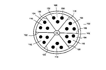
A preferred embodiment of the invention is
illustrated in Fig 1. The figure shows a composite
article 100 comprising a conductive jacketing layer 102
surrounding a matrix, 104, which substantially comprises
15 a noble metal. A plurality of discrete filament
decoupling layers 118, 120, 122, 124, 126, 128, 136 are
embedded in the matrix in an arrangement that separates
the matrix into a pluralit~ of, and preferably at least
three, separate domains 10~, 108, 110, 112, 114, 116.
20 Each decoupling layer is comprised of an insulating
material. In the fully processed article, the decoupling
layers separate the matrix into a plurality of
substantially electrically decoupled domains. A
plurality of filaments, 130, 132, 134, each comprising a
25 desired superconducting oxide or its precursors, are also
embedded within the matrix 104, so arranged that each
domain includes at least one filament, but each filament
is essentially encapsulated by the matrix. Thus, the
matrix chemically isolates each filament from the
30 decoupling layers and from any neighboring filaments.
The invention may be practiced with any desired
oxide superconductor or its precursors. By "desired
oxide superconductor" is meant the oxide superconductor
intended for eventual use in the finished article.
35 Typically, the desired oxide superconductor is selected
. . . ; . ~. ~ .
CA 02220930 1997-11-12
WO 9613648S PCT~US96~07061
-- 15 --
for its superior electrical properties, such as high
critical temperature or critical current density. By
"precursor" is meant any ]naterial that can be converted
to an oxide superconductor upon application of a suitable
5 heat treatment. Precursors may include any combination
of elements, metal salts, oxides, suboxides, oxide
superconductors which are intermediate to the desired
oxide superconductor, or other compounds which, when
reacted in the presence O:e oxygen in the stability field
10 of a desired oxide superconductor, produces that
superconductor. For example, there may be included
elements, salts, or oxides of copper, yttrium or other
rare earths, and barium for the rare earth family of
oxide superconductors; elements or oxides of copper,
15 bismuth, strontium, and calcium, and optionally lead, for
the BSCCO family of oxide superconductors; elements,
salts, or oxides of copper, thallium, calcium and barium
or strontium, and optiona:Lly, bismuth and lead, for the
thallium (TBSCCO) family of oxide superconductors;
20 elements, salts, or oxides of copper, mercury, calcium,
barium or strontium, and optionally, bismuth and lead,
for the mercury (HBSCCO) family of oxide superconductors.
The bismuth and rare earth families of oxide
superconductors are most preferred for operation of the
25 invention. By "oxide superconductor intermediate to the
desired oxide superconduc~or" is meant any oxide
superconductor which is capable of being converted to the
desired oxide superconductor. The formation of an
intermediate may be desired in order to take advantage of
30 desirable processing properties, for example, a micaceous
structure, which may not be equally possessed by the
- desired superconducting oxide. Precursors are included
in amounts sufficient to form an oxide superconductor.
~ In some embodiments, the precursor powders may be
35 provided in substantially stoichiometric proportion. In
CA 02220930 1997-11-12
W O 96/36485 PCTrUS96/07061
- 16 -
others, there may be a stoichiometric excess or
deficiency of any precursor to accommodate the processing
conditions used to form the desired superconducting
composite. For this purpose, excess or deficiency of a
5 particular precursor is defined by c- _~ison to the
ideal cation stoichiometry of the desired oxide
superconductor. Thalliation, the addition of doping
materials, including but not limited to the optional
materials identified above, variations in proportions and
10 such other variations in the precursors of the desired
superconducting oxides as are well known in the art, are
also within the scope and spirit of the invention.
The three-layer, high-Tc phase of a member of the
BSCCO family of superconductors (BSCCO 2223), such as
Bi2Sr2Ca2CU30X or (Bi, Pb)2Sr2Ca2Cu30x, is one of the
desired superconducting oxide most preferred for the
operation of the present invention. Composites including
BSCCO 2223 have demonstrated the potential for superior
meçhAn;cal and electrical performance at long lengths
20 when adequately textured. The current-carrying capacity
of a superconducting oxide composite depends
significantly on the degree of crystallographic alignment
and intergrain bonding of the oxide grains, together
known as "texturing", induced during the composite
~5 manufacturing operation. For example, known techniques
for texturing the two-layer and three-layer phases the
bismuth-strontium-calcium-copper-oxide family of
superconductors (BSCCo 2212 and BSCCo 2223, respectively)
are described in Tenbrink, WilAelm, Heine and Rrauth,
30 Development of Technical High-Tc Superconductor Wires and
Tapes, Paper MF-1, Applied Superconductivity Conference,
Chicago(August 23-28,1992J, and Motowidlo, Galinski,
Hoehn, Jr. and Haldar, Mechanical and Electrical
Properties of BSCCO Multifilament Tape Conductors, paper
CA 02220930 1997-11-12
W 096/36485 PCTAUS96107061
presented at Materials research Society Meeting, April
12-15, 1993.
The highest reported performance for BSCCO 2223
multifilamentary composite conductors has been obtained
5 in highly aspe~ted forms cont~;~;ng flattened filaments
with high aspect ratios. For untwisted or loosely
twisted conduct:ors, the AC losses in a highly aspected
tape are increased over the losses from a round wire of
equal cross-sec:tional area by (to a zero order
10 approximation) the square root of the tape's aspect
ratio. Thus, a tape with a 9:1 aspect ratio will have
about 81 times the losses of a round wire of e~ual cross-
sectional area. The high aspect ratios of the flattened
filaments also cause increased hyst;eretic losses in
15 transverse magnetic fields. If, as is typical, the tape
is obtained by deforming a round billet, filaments of
equal dimension will also be non-uniformly flattened by
the texturing process, with significantly greater
flattening and DIT texturing of filaments at the center
20 of the tape than of filaments at the periphery of the
tape and non-uniform distances between filaments causing
undesirable asymmetries in current carrying capability
and additional AC loss ef~ects.
The inventors have found that the division of the
25 matrix into a plurality oE substantially electrically
decoupled domains substantially improve the AC loss
characteristics of the superconducting composite article.
The effect is particularly pronounced for highly aspected
superconducting oxide composites, which have large eddy
30 current coupling losses when exposed to changing magnetic
fields normal to their wide faces. The inventors
believe that, by analogy t:o Carr's anisotropic continuum
model for losses in a mult:istrand Rutherford cable, W.~.
~ Carr, ~r. and V.T. Rovachev, "Interstrand eddy current
35 losses in SSC magnets," Cryogenics, submitted 1994., the
CA 02220930 1997-11-12
W O 96/36485 PCTrUS96/07061
- 18 -
losses in the filament/matrix region of an aspected
superconducting composite composed of multiple domains
can be a~p~oximated by a term representing the normal
conductance between adjacent filaments within a domain
B~ W2 L2
(~L +
12rn 4w2
plus a term representing the coupling losses along the
domain boundaries
B L2 1 w2
b
64 r~ ~2
In addition, the conductive jacket will have st~n~rd
10 eddy current losses, which can be approximated by
B2vw v
2 :r d
when the thickness of the jacketing layer is much smaller
than the strand ~;~~n~ions. If the layer separating
adjacent domains is an insulator whose resistivity far
15 exceeds the resistivity within the domain, Pperp will be
CA 02220930 1997-11-12
WO 96136485 PCTJUS96107061
-- 19 --
very low in co~np~rison tc P~ or Pj and may be ignored. If
one surface of the ~ ~; n is bounded by a portion of the
jacketing layer, then in the simplest case where only one
filament is folmd in each domain, the normal coupling Pn
5 will take place through the jacketing layer rather than
through the filament deccupling layers, and may be
represented by
B~ y2 l;2
~+-- )
6cZr 4 W2
m
This simplifiecl case will be approximated whenever there
10 are relatively few filaments per domain and the filament
decoupling layers have a resistivity at least 100 times
greater than that of the matrix . Thus, selective use of
discrete filament decoupling layers made from insulating
materials to establish substantially electrically
15 isolated domains significantly improves the AC loss
characteristice; of the multifilamentary composite.
In yet another aspect, the invention provides a
method of manufacturing a multifilamentary
superconducting composite article having improved AC loss
20 properties by i-irst, forming a composite intermediate
comprising mult:iple domains, each including one or more
fine, preferably twisted filaments of a superconducting
oxide material or its precursor, and then
ther~o~e~-h~n;ccllly processing the intermediate at
25 conditions sufi.-icient to produce at least one of the
effects of text;uring, crack healing and, if a precursor
to the desired superconducting oxide r~;n~, phase
~ transformation in the filament material under conditions
which support t:he electrical separation of the domains.
CA 02220930 1997-11-12
W 096136485 PCTrUS96/07061
- 20 -
In the preferred embodiment, the forming step includes
the step of providing filament decoupling layers
comprising insulating materials or their predecessors to
provide the desired domain separation.
Although the invention may be used to manufacture
these composite articles by processes such tape casting,
dip coating, and a variety of sputtering and vapor
deposition processes, it is particularly well-adapted for
manufacturing processes, such as powder-in-wire or the
10 well-known powder in tube (PIT) process, in which the
filament material is converted from precursor to desired
superconducting oxide while in intimate contact with an
enclosing matrix. The matrix material selected must be
readily formable and must be sufficiently non-reactive
15 with respect to the superconducting material that the
latter's properties are not substantially degraded in its
presence. Moreover, it must allow good oxygen access to
the filaments under the expected manufacturing conditions
to facilitate formation of the desired superconducting
20 oxides from their precursors. Metals which are noble in
that they are substantially non-reactive with respect to
oxide superconductors and their precursors and to oxygen
under the expected conditions (temperature, pressure,
atmosphere) of manufacture and use are preferred,
25 although alloys substantially comprising these metals,
including oxide dispersion strengthened (ODS) silver, may
also be used. Preferred noble metals include silver
(Ag), gold (Au), platinum (Pt) and palladium (Pd).
Silver and its alloys, being lowest in cost of these
30 materials, are most preferred for large-scale
manufacturing.
Fig 2 shows a process flow diagram for
manufacturing a composite article, such as that shown in
Fig 1, using PIT techniques in accordance with one aspect
35 of the present invention. In step 202, a monofilamentary
CA 02220930 1997-11-12
WO 96136485 PCT~US96~0706
- 21 -
rod is formed by packing a precursor oxide powder into a
metal container, such as a silver tube. In step 204,
the metal containers are deformation processed to form
monofilamentary rods of re~ diameter. In step 206, a
5 b~ g step, a number ~f the rods are assembled in some
close packed or other symmetric arrangement to form a
multifilamentary composite. Filament decoupling layers
are inserted among the rods in a predeter~;ne~ geometry
during the bunclling step. The layers may be in the form
10 of sheets, foils, cores, or other shapes depending on the
ultimate geometry desired. (For economies of scale, it
is preferred that the decoupling layers be assembled into
the composite at a relatively early stage of the
manufacturing process, while the desired superconducting
15 oxide is still in its more malleable precursor stage, but
this is not required for the practice of the invention.)
In accordance with a preferred embodiment of the present
invention, filament decoupling layers of predecessor
materials such as oxide forming materials selected from
20 the group consisting of the transition metals, the
alkaline earths, titanium, zirconium, niobium,
molybdenum, alum;nll~, and their alloys, may be selected.
In accordance with another preferred embodiment of the
invention, filament decoupling layers of insulating
25 materials such as alumina or other metal oxides,
nitrides, sulfides, semiconductors or intermetallics may
be selected. Step 206 is followed in step 208 by further
deformation processing including longitudinal reductions
and, for AC applications, preferably twisting, to form a
30 multifilamentary intermediate having the desired number
of filaments. A preferred deformation sequence is
drawing, then twisting, then rolling, but other
deformation sequences may be used.
Steps 206 and 208 may be repeated as many times as
35 desired, with the insertion of additional filament
CA 02220930 1997-ll-12
W O 96/36485 PCTrUS96/07061
- 22 -
decoupling layers at each iteration, to provide an
intermediate composite of reduced cross-section
including the desired number of ~o~; nc each defined by
one or more filament decoupling layers and containing one
5 or more twisted filaments of precursor material in
intimate contact with a ~L L ounding matrix, which
substantially comprises a noble metal,. From one to five
rebundling iterations are preferred. Turning now to Fig
3, a highly aspected superconducting tape 300 is shown,
10 which may be manufactured by rebundling intermediates
with one filament per domain, made in the general form of
intermediate 100 shown in FIG 1 above with additional
decoupling layers 304, 306, 308, and inserting the whole
ensemble into a jacketing layer 302 for deformation and
15 ther~ ~ch~n; cal processing as described above.
The conductive jacketing layers shown in Figs 1
and 3 may be added to the intermediate during or after
steps 206, 208, or 210. The material for the jacketing
layer must have an electrical resistivity at least equal
20 to, and preferably 10 times that of the matrix material.
Resistivities on the order of 0.5 -10 mohm cm are
especially preferred. However, because the jacketing
layer is chemically isolated from the filaments by the
matrix, it may be somewhat reactive with respect to the
25 superconducting material under expected manufacturing
conditions. In the preferred embodiments made using a
PIT process, it must also be readily formable and must
allow good oxygen access to the filaments under the
expected manufacturing conditions. Preferred jacketing
30 materials include silver and other noble metals, and
their alloys, particularly ODS silver and silver-gold
alloys. In one embodiment, the matrix and jacketing
layer may be formed simultaneously from the same noble
metal, and a post-processing step added to increase the
CA 02220930 1997-11-12
WO 96/36485 PCT~US96/07061
-- 23 --
resistivity of the jacketing layer by, for example, ion
bombardment.
In step 210, the intermediate is
therm~ ?ch~n;cally processed at conditions sufficient to
5 produce at least one of t;he effects of texturing, crack
healing and, if a precursor to the desired
superconducting oxide r~;n~, phase transformation in
the filament ma~erial under conditions which su~o~ the
electrical sepaxation of the domains. In the
10 preferred embodiment in which the filament decoupling
layers comprise a predecessor to an insulating material,
the intermediate is ther~t ?chAn;cally processed at
conditions sufficient to produce at least one of the
effects of passivating any predecessor material and
15 forming an insu:Lating material in the decoupling layers
and texturing, crack healing and, if a precursor to the
desired superconducting oxide re~; n~, phase
transformation in the filament material. Typically, in
this case, the thermomech~;cal processing step comprises
20 the steps of first heat treating the composite at
conditions sufficient to passivate the pr~ec~or and
form an insulating material from at least part of the
predecessor material but not to activate the filament
materials, and, thereafter activating the filaments by
25 thermomechanical treatment at conditions sufficient to
produce at least: one of the effects of texturing, crack
healing and, if a precursor to the desired
superconducting oxide r~;n~, phase transformation in
the filament mat:erial. By "conditions which activate the
30 filament materials" are meant conditions which enable
substantial chemical and/or thermodynamic phase
- transformations in these materials (but not the matrix).
By "texturing", as that term is used herein, is meant
inducing crystallographic alignment and intergrain
CA 02220930 1997-11-12
W 096/36485 PCTrUS96/07061
bonding of the grains of a desired superconducting oxide
or its precursors.
In one preferred embodiment of the invention, the
preliminary heat treatment step is continued until the
5 metal predecessor layers are essentially passivated by
thorough oxidation of the interface between the metal
predecessor layers and the adjoining matrix before any
substantial thermomec-h~n;cal activation of the precursors
takes place. Passivation may take place either by
10 formation of an oxide scale on these surfaces or by
essentially complete oxidation of the entire metal
predecessor layer. For inteL ~~;~tes containing
precursors to the copper oxide high temperature
superconductors, prel;m;n~ry heat treatment in an
15 oxidizing atmosphere at a temperature of less than about
700 degrees C, and preferably less than about 550 C, for
up to 100 hours has been found to adequately oxidize the
predecessor layers under conditions where the precursors
are kinetically limited. Therml ?ch~n;cal activation of
20 the intermediate may then be performed in accordance with
conventional PIT processing methods.
In another preferred embodiment of the invention,
passivation may not be completed until thermomechanical
activation of the precursors has begun, but the
25 predecessor materials and passivation conditions may be
selected so that the oxygen flux associated with the
passivation reactions does not interfere with the
desired phase evolution of the precursors, for example,
by annealing at very high oxygen pressures, preferably
30 greater than about 10 atmospheres.
FIGs 4, 5 and 6 are schematic diagrams of three
alternative processing sequences for the prel;m;n~ry heat
treatment and thermomech~n;cal filament activation steps
in accordance with these preferred embodiments of the
35 invention. As shown in FIG 4, a separate prel;m;n~ry
CA 02220930 1997-11-12
W O 96136485 PCTAU~J'~61
- 25 -
heat treatment step 402 may be done at a fixed
temperature prior to the initiation of thermomec!hAn;cal
activation 404. Alternatively, the preliminary heat
treatment may take place during the ramp-up 502 to
5 the, c-h~n;cal activation conditions, 504, with one or
more plateaus, as illustrated by FIG 5, or continuously,
but at a very slow ramp rate, preferably less than 10
C/min as illustrated by 602 in FIG 6. In each
processing sequence, the duration of the prel;m;n~ry heat
10 treatment step will determine whether the predecessor is
fully passivated prior to activation of the filament
material. Upon completion of passivation, at whatever
point in the sequence this takes place, thermomechanical
activation may be continued as required to obtain optimal
15 performance in the superconducting composite.
In the preferred embodiment in which the filament
decoupling layers comprise an insulating material, the
thermomeçh~;cal processing step comprises the step of
texturing, crack healing and, if a precursor to the
20 desired superconducting o~ide remains, phase
transformation in the filament material at conditions
selected so that any activation of the insulating
material does not significantly impair its insulating
properties or interfere with the desired phase
25 transformations of the filament materials. In this
embodiment, selection of an appropriate insulating
material is essential. In addition to high relative
resistivity and inertness to both the filament material
and the matrix material under the conditions of
30 manufacture, the insulating material must be flowable
enough to handle the substantial deformations typical of
superconducting composite manufacturing processes.
Relatively few insulating materials possess either a work
hardening rate or a strain rate sensitivity which provide
35 sufficient flowability in combination with the other
CA 02220930 1997-11-12
W 096/36485 PCTrUS96/07061
- 26 -
required characteristics. Powders or bulk forms of boron
nitride, tungsten carbide, titanium carbide, silicon
carbide, alumina, silicon nitride, boron carbide,
zirconium oxide, titanium nitride, yttrium oxide, or
5 magnesium oxide may be used.
FIGs 7 and 8 illustrate alternate forms of
multifilamentary composite articles manufactured in
accordance with the invention. As shown in Fig 7, the
matrix portion 704 of round composite wire 700 is
10 separated into a plurality of separate domains 718, 720,
722, 724, 726 by multiple filament decoupling layers 706,
708, 710, 712. The filament decoupling layers have a
closed geometry in that each forms a closed loop in
cross-section which completely encloses the cross-
15 sections of one or more filaments 714, 716. The materialfor the filament decoupling layers is selected to be a
material which is oxygen permeable under the activation
conditions for the filaments. For example, zirconium or
zirconium oxide filament decoupling layers may be used in
20 combination with BSCC0 2223 filaments. In the embodiment
shown, a plurality of filaments are embedded in each
domain but in an alternate embodiment, each domain might
contain a single filament. A jacketing layer 702 of
conductive material surrounds the matrix. In an
25 alternate embodiment, the jacketing layer may be a
composite material including both conductive and non-
conductive portions.
Turning now to Fig 8, a highly aspected tape 800
is shown in which filament decoupling layer 806 forms a
30 central spine and additional filament decoupling layers
form radiating legs 808, 810, 812, 814, 816, 818, 820,
822, 824, 826, 828, 830 which separate the matrix 804
into domains 838, 840, 842, 844, 846, 848, 850, 852, 854,
856, 858, 860 each containing one or more filaments, for
35 example filament 832, of superconducting oxide material
CA 02220930 1997-11-12
W~ 96136485 PCT~US96/07061
As shown in Fig 9, a tape in this form may be
manufactured in accordance with the invention by first,
forming a hollow tube having an outer wall 804 of a
suitable matrix material and an inner wall comprising a
5 filament decou~ling layer 806; second, forming an
intermediate by inserting additional filament decoupling
layers 808, 810, 812, 814, 816, 818, 820, 822, 824, 826,
828, 830 at spaced intervals between the inner and outer
walls of the tube and filling the rem~;n;ng area inside
10 the tube with the precursors of a desired superconducting
oxide to form filaments, for example filaments 832, 834,
836. (One or more filaments may be included in each
~o~;n.) ; next, deforming the intermediate to flatten
the tube, twist the filaments and texture the material
15 comprised therein; and finally, therm~ ?ch~n;cally
processing the intermedial:e as described above. In one
aspect of the invention, microcracking of the filament
decoupling layers during t:he deformation step may provide
improved oxygen access to the filaments during
20 thermo~Ach~nical processing.
A round wire is shown in FIG 7 and a rectangular
tape is shown in FIG 8, but articles in a variety of
forms may be manufactured in accordance with the
invention. Round filaments are shown in Fig 7 and 8 but
25 any aspect ratio and any cross-section, such as square,
hexagonal, octagonal, or trapezoidal, may equally be
used. For superior AC performance, fine filaments should
be used. By "fine filaments" are meant filaments with a
maximum transverse cross-sectional dimension less than
30 750 , and preferably less than 150 microns. High aspect
ratio filaments~ with an aspect ratio of about 10:1, and
a thickness less than about 75 microns, may be used.
In manufacturing the superconducting composite
- articles in accordance with one aspect of the present
35 invention, precursor powders and composite subunits may
CA 02220930 l997-ll-l2
W 096136485 PCTnUS96/07061
- 28 -
be formed using one of the st~n~rd PIT t~chn;ques. For
example, nitrate powders comprising the precursors of
BSCCO 2223 may be packed in st~n~Ard silver billets, and
extrusion and wire-drawing may be used to form hexagonal
5 monofilamentary rods. A plurality of these rods may be
assembled in a close-packed manner, and filament
decoupling layers of oxide forming materials preferably
selected from the group consisting of zirconium, niobium,
molybdenum and their alloys may be inserted among the
10 rods in a predetermined geometry to define a plurality of
separate domains. The assembly steps may be repeated as
often as required to obtain an intermediate composite
with the desired number and arrangement of domains such
as, for example, those shown in FIGs 1, 6 or 7. If a
15 jacketing layer is desired, the entire assembly may be
inserted into a conductive tube. Composites with up to
10,000 domains, but only a small number of fine filaments
per domain, are preferred. A succession of deformation
steps, including but not limited to drawing, twisting and
rolling, may be used to reduce the diameter of the
intermediate to a value in the range of from 0.01 inch to
0.12 inch (0.025 to 0.3 cm), and preferably 0.02 inch to
0.06 inch (0. 05 to 0.153 cm), and to obtain a desired
twist pitch, preferably at least on the order of the
width of the intermediate. In a preferred embodiment,
the intermediate may be wire- drawn to a diameter in the
range of 0.15 inch to 0. 02 inch (0. 038 to 0.05 cm)
twisted to about 20 twists per inch (a twist pitch of
1.25 mm) and then rolled in one or more reduction passes
to a ma~;~llm transverse cross-sectional ~ ion in the
range of 0. 05 inch to 0. 005 inch (0.127 to 0. 013 cm)
If multiple deformations are performed, intermediate
anneals will preferably be performed in between. In
accordance with the invention, the intermediate may be
subjected to a prel;m;n~ry heat treatment step in an
CA 02220930 1997-11-12
WO 96/3648S PCT~JS96tO706
-- 29 --
oxidizing atmosphere at a temperature of less than about
700 degrees C, and preferably less than about 550 degrees
C, for up to 10~ hours in order to oxidize the decoupling
layers under conditions where the BSCCO precursors are
5 kinetically limited. The intermediate may then be heat
treated at 750 ~370 C for ~-100 hours at 0.001 to 1
atmosphere oxygen to promote texturing and achieve proper
oxygenation of the BSCCO precursors. Then a final heat
treatment may be performed in a 7.5% oxygen atmosphere
10 at 828 to 832 C for 20 to 80 hours, 805 to 815 C for 1 to
240 hours and 7~37 to 795 C for 10 to 50 hours to form and
sinter the desired 2223 material in the filament cores
and to promote c~rack healing.
The invention may be further understood from the
15 following examples:
EXAMPLES 1 - 8
M~O~M~NT ROD FORMATION
Precursor powders were prepared from the solid
state reaction of freeze-dried precursors of the
20 appropriate metal nitrates having the nominal composition
of 1.8:0.3:1.9:2.0:3.1 (Bi:Pb:Sr:Ca:Cu). Bi2O3, CaC~3,
SrCO3, Pb304 and CuO powders could equally be used.
After thoroughly mixing the powders in the appropriate
ratio, a multistep treatment (typically 3-4 steps) of
25 calcination (800~C+ 10~C, Ior a total of 15 h) and
intermediate grinding was performed in order to remove
residual carbon, homogenize the material and generate a
BSCCO 2212 oxide superconductor phase.
The powders were packed into silver sheaths having
30 an inner diameter of 0.850 inch (2.16 cm) and a length of
8 inch (20.32 cm) and an outer diameter of 1.25 inch
3.18 cm) to form a billet:. The billets were extruded
to a diameter of 1/2 inch ~1.27 cm). The billet diameter
was narrowed with multiple die steps, with a final step
,
CA 02220930 1997-11-12
W 096/36485 PCTrUS96/07061
- 30 -
drawn through a 0.70 inch (1.78 cm) hexagonally shaped
die into a silver/precursor hexagonal wires.
INTERMEDIATE FORMATION
Eighteen of the wires were bundled together around
5 a central nickel rod with a diameter of 0.070 inch (0.18
cm), which had previously been Ann~Aled for 2 hours at
600 C in a reducing atmosphere, and six nickel sheets,
each made from a double thickness of 0.005 inch (0.013
cm) nickel foil (99.7% pure) were inserted among the
10 wires to form six dom~;n~ contA;n;ng three wires each. In
order to make a control composite, nineteen of the same
wires were bundled together without nickel insertions.
The two assemblages were inserted into opposite ends of a
silver sheath having an inner diameter of 0.387 inch (
15 0.98 cm) and an outer diameter of 0.42 inch (1.06 cm) to
form a billet. The billet was drawn to 0.18 inch (0.46
cm) via successive 20% pass reductions and then annealed
at 450 C in air for 4 hours, drawn to 0.072 inch (0.183
cm) via successive 20% and 10% pass reductions, annealed
20 at 450 C in air for 2 hours, and finally drawn to Ø04
inch ( 1.02 cm) and annealed at 450 C in air for 4 hours
to form a multifilamentary round intermediate. Two
nickel-contA;n;ng and two control portions (OX1026N with
filament decoupling layers and OX1026 without) were then
25 taken from the intermediate.
EXaMPLES 1-4
The first part of each was not twisted before it
was rolled to a final thickness of 0.010 inch (0.25 cm)
via a single reduction pass. It was then further
30 separated longitudinally into 4 sections (Examples 1-4).
Example 1 was ramped up to 400 C at 10 C/minute, to 700 C
at 1 C/minute and then to 830 C at 0.1 C/minute in a
7.5% oxygen atmosphere and immediately given a final heat
treatment in a 7.5~ oxygen atmosphere at 830 C for 40
35 hours, 811 C for 40 hours and 787 C for 30 hours to form
CA 02220930 1997-11-12
W O 96/36485 PCT~US96/07061
- 31 -
and sinter the desired 2223 material in the filament
cores and produce a thin nickel oxide layer. Example 2
was ramped up t:o 500 C at 10 C/minute and immediately
given a short high oxidation treatment at 500 C for 4
5 hours in a lOO~i oxygen atmosphere, then equilibrated at
500 C for 4 houLrs in a 7.5~ oxygen atmosphere, followed
by a ramp up to 830 C at 1 C/minute and the same final
heat treatment used for Example 1, to form and sinter the
desired 2223 material in the filament cores and produce a
10 moderate nickel oxide layer. Example 3 was ramped up to
500 C at 10 C/minute and ;~mP~; ately given a long high
oxidation treatment at 500 C for 4 hours in a 100% oxygen
atmosphere and then equilibrated at 500 C for 16 hours in
a 7.5~ oxygen atmosphere, followed by followed by a ramp
15 up to 830 C at 1 C/minute and the same final heat
treatment used for Example 1 to form and sinter the
desired 2223 material in 1:he filament cores and produce a
thick nickel oxide layer. Example 4 was ramped up to 450
C at 10 C/minute and then to 500 C at 2 C/minute in 100%
20 oxygen atmosphere and given a high pressure oxidation
treatme3nt at 500 C for 20 hours at 100 atm (1500 psi),
allowed to equilibrate to room temperature and pressure
and then ramped up to 350 C at 10 C/minute and then to
400 C at 2 C/minute in 100% oxygen atmosphere and given
25 an equilibration cycle at: 400 C for 40 hours at 7.5%,
followed by the same final heat treatment used for
Example 1 to form and sinter the desired 2223 material in
the filament cores and produce a very thick nickel oxide
layer.
After the final heat treatment, the critical
current of Examples 1-3 were measured at 77K, using a 1
mV/cm criteria and a 1 cm voltage tap length. The
critical currenls of the experimental conductors were
- determined usinq a four-point probe technique.
35 Engineering crit:ical current densities were calculated
CA 02220930 l997-ll-l2
W 096/36485 PcTru~Gl~7~6
- 32 -
for all samples as the measured critical current
separated by the cross-sectional area of the wire.
Averages reported are the averages of two samples. N
indicates the samples which included filament decoupling
5 layers. Thickness and width measurements are in inches.
Wire ID Thickness Width Ave Je Ave
Jc
Ex lN 0.0105 0. 084 322 1109
Ex 2N 0.01 0.084 474 1635
EX 3N 0.0104 0.081 780 2690
EX 1 0.0104 0.07 1094 3388
EX 2 0.0099 0.067 2048 6341
The results show that composites cont~;n;ng filament
decoupling layers can be made to superconduct, and
15 suggest that increased oxidation provides increased
engineering critical current density, whether or not the
samples include a filament decoupling layer.
EXAMPLES 5-8
The second part of the nickel-cont~;n;ng
20 intermediate (OX1026NAT) was twisted to 3.0 twists/inch
(1.181 twists/cm) using a hand drill and then rolled to a
final thickness of 0.010 inch (0. 025 cm) via successive
5% thickness reduction passes with 2 intermediate
anneals - 1 hour at 450 C in air at a thickness of
25 0. 025 inch (0. 063 cm) and 4 hours at 450 C in air at a
thickness of 0.156 inch (0.053 cm) to form an
intermediate article.
EXAMPLE 9
A multifilamentary composite intermediate article
30 may be made using filament decoupling layers in the form
of insulating materials and the intermediate then
processed to form a superconducting composite. Boron
nitride or tungsten carbide powders may be packed into
CA 02220930 1997-11-12
WO 96/36485 PCT/US96/0706
six silver sheaths, each having an inner diameter of
0.850 inch (2.16 cm) and a length of 8 inch (20.32 cm)
and an outer diameter of 1.25 inch (3.18 cm) to form
six billets. Alternativel~r, powders of titanium carbide,
5 silicon carbide, alumina, silicon nitride, boron carbide,
zirconium oxide, titanium nitride, yttrium oxide, or
magnesium oxide may be used. Each billet may be drawn by
a series of 10% reduction passes to a diameter of 0.200
inch (0.51 cm) and then rolled by a series of 10%
lo reduction passes to a tape with a thickness of 0.005 inch
(0.013 cm). Each of these tapes may be used as a
f;l~ ?nt decoup:Ling layer.
Hexagonal monofilal!nentary wires of silver/BSCC0
2223 precursor T~ay be prepared as described in Examples
15 1-8. Each of t~le tapes may be bent into the shape of a
gutter and three wires placed in it. Then the six bent
tapes may be bundled together, with their open sides
facing outwards, around a central silver rod with a
diameter of 0.070 inch (0.178 cm), to form six separate
20 do~;n~ con~A;n;ng three wires each, and the entire
assembly inserted into a tubular silver jacketing layer
having an inner diameter of 0.387 inch (0.982 cm) and an
outer diameter of 0.42 inclh (1.067 cm) to form a billet.
The billet may be drawn to 0.18 inch (0.457 cm) via
25 successive 20% pass reductions and then annealed at 400 C
in air for 1 hour, drawn to 0.072 inch ( cm) via
successive 20% and 10% pass reductions, annealed at 400 C
in air for 1 hour, and finally drawn to Ø04 inch
0.102 cm) and annealed at 400 C in air for 1 hour to form
30 a multifilamentary round intermediate. Since the
insulating materials in the filament decoupling layers
will already be :~ully passivated, Example 9 may be
thermor~ch;ln;cal:Ly processed by ramping up to 830 C at 1
C/minute in a 7 5g6 oxygen atmosphere and immediately
35 giving a final heat treatment in a 7.5% oxygen atmosphere
.
CA 02220930 l997-ll-l2
W 096/36485 PCTrUS96/07061
- 34 -
at 830 C for 40 hours, 811 C for 40 hours and 787 C for
30 hours to form and sinter the desired 2223 material in
the filament cores.
EXAMPLB 10
A multifilamentary YBC0 composite intermediate
article may be made using filament decoupling layers in
the form of alumina scale formers and the intermediate
then processed to form a superconducting composite. In
this embodiment, the precursor may be prepared as
10 described in U.S. Patent No. 5,034,373 or US Patent
Application S.N. 07/881,675 filed 5/12/92, which are
incorporated herein by reference. An alloy of Y-Ba-Cu-Ag
or Y(Ca)-Ba-Cu-Ag, with, preferably the appropriate
stoichiometry of metallic constituents to form a 1-2-4
type oxide superconductor, may be packed as a powder into
a silver sheath having an inner diameter of 0. 05 inch
(1.25 cm), a length of 8 inch (20.32 cm), and an outer
diameter of 0.06 inch (1. 57 cm) . Silver powder,
typically comprising 10-50 weight ~ of the total powder,
should be included with the alloy. The packed billet may
be welded shut under a protective atmosphere and then
reduced in diameter by warm hydrostatic extrusion at 325C
to form monofilamentary wires.
Eighteen of the wires may be bundled together
around a central aluminum/copper alloy rod tl~% aluminum,
90% copper] with a diameter of 0. 070 inch (0.18 cm),
which had previously been annealed for 2 hours at 600 C
in a reducing atmosphere, and six sheets of the same
aluminum/copper alloy, each made from a double thickness
of 0. 005 inch (0.127 cm) foil (99. 7% pure) may be
inserted among the wires to form six dv ~; n~: contA; n;ng
three wires each. The bundle may be drawn to 0.18 inch
(0.46 cm) via successive 20% pass reductions and then
annealed at 450 C in air for 4 hours, drawn to 0.072 inch
CA 02220930 1997-11-12
W O 96136485 PCT~US96J07061
- 35 -
(0.18 cm) via ~successive 20% and 10% pass reductions,
annealed at 450 C in air for 2 hours, and finally drawn
to Ø04 inch ( 0.10 cm) and ~nne~led at 450 C in air for
4 hours to form a multifilamentary round intermediate.
5 The intermediates may be rebundled with additional
al~- ;nllm/copper alloy sheets and rods, and the reduction
process repeated as often as desired to obtain an
intermediate oi- the desired ~i-?n~ions with the desired
number of doma~ns. The resulting intermediate may be
10 thermome~h~n;cally processed by oxidizing in pure oxygen
at 500 C for 300-400 hours, and then deformed at room
temperature by 2 to 6 iterations of, for example,
pressing at 13,000 to 35,000 pounds load force or rolling
by successive ~0 to 20% pass reductions alternating with
15 anneals for 0.~ to 10 hours at 650-800 C to obtain a
multifilamentary superconducting composite.
EXAMPLE 11
A multifilamentary BSCCO 2212 composite
intermediate article may be made using closed zirconium
20 filament decoupling layers and the intermediate then
processed to form a superconducting composite. In this
embodiment, the precursor may be prepared as described in
Phase Alignment in Ag-Clad 2212 Bi-Sr-Ca-Cu-O Wires, R.
D. Ray II ~ E. E. Hellstrom, Appl ied Physics Letters, 57,
25 2948-29~0 (199OJ, which is incorporated herein by
reference. Precursor powders may be prepared from
reagent grade Bi2o3~ CaCO3 SrCO3, and CuO powders with a
nominal Bi:Sr:Ca:Cu mole ration of 2:2:1:2. After
thoroughly mixing the powders in the appropriate ratio, a
30 multistep treatment (typically 3-4 steps) of calcination
(800~C - 825~C, for a total of 48 h), isostatic pressing
(280 MPa) and intermediate grinding may be performed in
order to remove residual carbon, homogenize the material
and generate a BSCCO 2212 oxide superconductor phase.
CA 02220930 1997-11-12
W 096/36485 PCTrUS~G~'~7-~1
- 36 -
The powders may be packed into zirconium-coated
silver sheaths having, for example, an inner diameter of
0.850 inch (2.16 cm) and a length of 8 inch (20.32 cm)
and an outer diameter (silver layers) of 1.25 inch (3.18
5 cm) and a sputtered 2 micron thick outer coating of
zirconium to form billets and drawn to 0.055 inch (0.138
cm) via one or more pass reductions, with one or more
intermediate anneals at 400 C in air for 1 hour.. Six of
the billets may be bundled together around a central
lO silver rod with a diameter of 0.070 inch (0.18 cm) and
the entire assembly inserted into a tubular silver
jacketing layer having an inner diameter of 0.170 inch
(0.43 cm) and an outer diameter of 0.210 inch (0.53 cm)
to form a composite billet. The billet may be drawn to a
15 0.055 inch (0.138 cm) diameter round via one or more pass
reductions with one or more intermediate anneals at 400 C
in air for 1 hour, twisted to a 2.54 inch (1 cm) twist
pitch, annealed as before, and finally rolled to a final
cross-section of about 0.12 inch (0.3 cm) by 0.004 inch
(0.01 cm) to form a multifilamentary intermediate
article.
The intermediate may be heated at 5C/min to 920 C,
held for 15 minutes, cooled at 10 to 240 C to 840 C,
annealed at 840 C for 70 hours, all in air and finally
25 air cooled at room temperature to obtain a
multifilamentary superconducting composite tape.
The various features and advantages of the
invention may be seen from the foregoing description.
Iterative variations on the processes described above,
30 such as changes in the parameters, number and order of
the torsional and conventional texturing steps will be
seen to be within the scope of the invention. Many
modifications and variations in the preferred embodiments
illustrated will undoubtedly occur to those versed in the
35 art, as will various other features and advantages not
CA 02220930 1997-11-12
WO 96136485 PCT~US96~0706
specifically enumerated, all of which may be achieved
without departing from the spirit and scope of the
invention as defined by the following claims.
What is claimed is: