Note: Descriptions are shown in the official language in which they were submitted.
CA 0222144~ 1997-11-18
W096/37042 PCT/~--'n0~26
METHOD AND APPARATUS FOR TR~N-~M I ~ l~G SIGNALS IN AN OPTICAL
FIBRE
~ TECHNICAL FIELD
The invention relates, on the one hand, to a method for
transmitting signals in an optical fibre, comprising amplitu-
de modulating an optical carrier at a high frequency with the
signals to be transmitted, and transmitting the so modulated
optical carrier in the fibre, and, on the other hand, to an
apparatus for transmitting signals in an optical fibre,
comprising an amplitude modulator for amplitude modulating an
optical carrier at a high frequency with the signals to be
transmitted.
BACRGROUND OF THE lNV ~:wllON
One of the main problems with high frequency or high speed
fiber-optic transmission systems, 10 Gbits/s and above, in
development nowadays, is the group velocity dispersion in the
fiber which distorts the transmitted signal. Most of the
installed fibers have zero dispersion at 1.3 ~m, but minimum
loss at 1.55 ~m, where the group velocity dispersion is about
-17 ps/(nm.km). This distortion is already a problem at 2.5
Gbit/s for long distance transmission, above 100 km, where it
necessitates the use of external modulators instead of
directly modulated semiconductor lasers. At 10 Gbit/s,
dispersion is the main limiting factor for the transmission
distance and this gets worse at higher bit rates since the
spectral spreading of the signal is proportional to the bit
rate.
The reason why dispersion distorts the signal is that it
introduces a phase varying as the square of the modulating
frequency. Both side-bands get this phase with the same sign.
After detection by a square-law detector, such as a photodio-
de, this results in a small-signal response of the form:
H(~) = cos(F L~2) (1)
where v is the modulation frequency and L the tr~n! ;~sion
CA 0222144~ 1997-11-18
WO 96/37042 PCT/SE96/00626
distance, which introduces zeroes of transmission in the band
of frequencies of interest if L becomes large enough. These
zeroes are responsible for the distortion of the signal.
Since the problems increase with the spectral width of the
signal being transmitted, one way to improve the situation
would be to limit this spectral width. In the radio and TV
domain, spectral reduction is used to pack more channels in
the available frequency bands and is often done with Single-
Side-Band (SSB) modulation, with or without carrier suppres-
sion, or with Vestigial Side-Band (VSB) modulation. The
problem with carrier suppression is that a very stable,
narrow-band local oscillator is needed to recover the signal.
This makes it similar to coherent modulation systems (FM, PM)
but commercial optical transmission systems nowadays use
exclusively Amplitude Modulation (AM) because a simple
square-law detector, such as a photodiode, can then be used
at the receiver.
Other methods have been proposed previously to overcome the
problems caused by dispersion in fibers. The two most pro-
mising ones seem to be spectral inversion by four-wave mixing
and use of a length of fiber with opposite sign of the
dispersion. The problem of spectral inversion is that it is
fairly complex, has a low efficiency, must be implemented in
the middle of the fiber link and is difficult to use in a
wavelength multiplexed system. The main problem with the
compensating fiber is the additional losses which must be
compensated with an optical amplifier and thus cause a
degradation of the signal-to-noise ratio.
BRIEF DESCRIPTION OF THE lNv~..lON
The object of the invention is to overcome, in the optical
~r_ '; n, in a simple manner and at a low cost, the limitation
in transmission distance due to group velocity dispersion in
optical fibers.
This is attained by the method according to the invention by
suppressing at least part of one of the side bands of the
CA 0222l44~ l997-ll-l8
wos6l37o42 PCT/SE96/00626
modulated optical carrier to reduce the effect of group
velocity dispersion in the optical fibre.
This object is also attained by the apparatus according to
the invention in that it comprises a suppressing means for
suppressing at least part of one of the side bands of the
modulated optical carrier to reduce the effect of group
velocity dispersion in the optical fibre.
This side band suppression can be done before transmission in
the fibre or, alternatively, after transmission in the fibre
but before detection of the optical signal.
An electric circuit for phase correction (and eventually
equalization) can also be added to the receiver.
The method and apparatus according to this invention are
simple and can be implemented at low cost, which makes them
competitive with methods and apparatuses proposed so far.
BRIEF DESCRIPTION OF THE DRAWING
The invention will be described more in detail below with
reference to the appended drawings on which
Fig. 1 shows a first embodiment of an apparatus according to
the invention,
Figs. 2a and 2b show diagrams illustrating the function of
the embodiment according to Fig. 1,
Fig. 3 shows a second embodiment of the apparatus according
to the invention,
Figs. 4a, 4b and 4c show diagrams illustrating the function
of the embodiment according to Fig. 3,
Fig. 5 shows a third embodiment of the apparatus according to
the invention, and
CA 0222144~ 1997-11-18
WO 96137042 PCT/SE96100626
Figs. 6a, 6b and 6c show diagrams illustrating the function
of the embodiment according to Fig. 5.
DET~TT~F!n DESCRIPTION OF THE lNvlsN~lloN
To attain the object of the invention, i.e. retain the cost
and reliability advantages of a simple receiver, either
simple SSB or VSB is used according to the invention.
Further analysis of the SSB and VSB modulation schemes shows
an even larger benefit than just the reduction of the spect-
ral extension of the signal.
In a pure SSB system, however, there is only one side band
and the response becomes:
HSSB(~) = (1/2)exp(j F Lv2) (2)
where j is the square root of -1, which is a pure frequency
dependent phase. This can be compensated by an electrical
circuit performing a phase correction.
Real SSB iS difficult to implement in the optical domain. In
addition, simulations of the transmission of pseudo-random
bit patterns with large extinction ratio for the modulation,
which is the way AM modulation is usually done in optical
systems, show that pure SSB modulation may not be the best
solution.
However, the three VSB modulation embodiments of the appara-
tus according to the invention to be described below, give a
significant improvment of the achievable transmission distan-
ce.
The three embodiments of VSB optical modulators to be descri-
bed are based on the use of an asymmetric Mach-Zehnder
interferometric filter (Fig. 1), a Bragg grating filter (Fig.
3) and a Fabry-Perot filter (Fig. 5), respectively.
Other embodiments of the VSB modulator can be trivially
CA 0222l44~ l997-ll-l8
W096/37042 PCT/SE96/00626
obtained by using a different type of optical filter instead
of one of the three listed above. Examples include multilayer
dielectric filters, interference filters, double Fabry-Perot
filters and so on. The only requirement is that the filter
suppresses most of one of the side bands while transmitting
most of the carrier and the other side band.
As an alternative to the VSB modulator, it is also possible
to use instead a normal amplitude modulator of one of the
types described below and to perform the filtering of the
optical signal at the receiver, after transmission in the
fibre. The problems and advantages of this solution are
discussed below.
In all cases, an electric circuit for phase correction of the
received signal may be required, as shown by equation (2).
However, some of the optical filters, such as the Fabry-Perot
filter also add a phase to the optical signal, which may make
the electric phase correction unnecessary. In addition, an
equalization of the electric signal may be advantageous in
some cases. This is because most of the filters will not only
add a phase, as in the SSB case described by equation (2),
but also modify the amplitude (see for example equation (8)
below for the asymmetric Mach-Zehnder filter).
VSB modulators
The three embodiments of VSB modulators to be described here
are all based on the use of an amplitude modulator and an
optical filter. Other methods for obtaining a VSB (or SSB)
modulator are known but are either more difficult or impos-
sible to implement at very high bitrates or more complicated
and expensive.
Below, it is assumed that the modulator itself does a pure AM
modulation (no chirp). This is possible both with semiconduc-
tor electro-absorption modulators and also with symmetric
Mach-Zehnder modulators (implemented in LiNbO3 or a semicon-
ductor).
CA 0222144~ 1997-11-18
WO 96137~42 PCT/SE:96100626
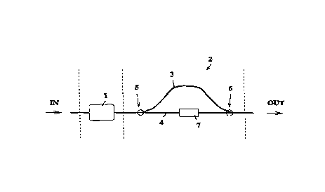
The apparatus shown in Fig. 1 comprises an amplitude modula-
tor l for amplitude modulating an optical carrier IN at high
speed with the signals to be transmitted towards the recei-
ving end. According to the first embodiment of the apparatus
according to the invention, the modulator 1 is followed by an
asymmetric Mach-Zehnder interferometer, generally denoted 2,
having two arms, a longer arm 3 and a shorter arm 4, between
a splitter 5 and a combiner 6.
Three parameters to be described below are important for the
correct operation of this device:
1. The two arms 3 and 4 of the interferometer 2 must have
nearly equal losses so that an out-of-phase recombination in
the combiner 6 will result in a large extinction ratio. Due
to absorption and scattering, the longer arm 3 will usually
have higher losses. Several compensation methods are pos-
sible, depending on the material and fabrication method used
to make the device. One method that is applicable in general
is to use an asymmetric splitting ratio at the splitter 5 in
the interferometer 2 so that the powers are equal at the com-
biner 6. Another method is to have an additional loss or gain
in one of the arms 3 and 4 to equalize the total losses.
2. The optical path difference between the two arms 3 and 4
will determine the filter characteristics, since its transfer
function can be written as:
TMZ(~)= ~1 + exp(j Pl P2 ~)~ (3)
where the losses are neglected and ~ is the angular frequency
of the light, c is the speed of light and Pi is the optical
path length of one arm of the interferometer 2, defined as:
Pi =lArmine~(s)dS (4)
where s is the distance along the arm and neff is the effec-
tive propagation index for the light in that arm. If neff is
the same and constant everywhere, equation (3) reduces to:
CA 0222144~ 1997-11-18
WO 96/37042 PCT/SE96/00626
TMz(~)= ~[1 + ej0 exp~ (5)
where ~d is the length difference between the arms and 0
accounts for any additional phase difference, due for example
to a phase control device 7 in one of the arms.
From equation (3) or (5), we can see that the filter transfer
function is periodic in ~ and that the period depends on the
optical path difference (or Ad).
3. The relative position of the carrier frequency ~0 and the
maxima and minima of transmission of equation (3) is very
important for a good operation of the device. For example, if
~0 coincides with a minimum, no signal is transmitted and if
it coincides with a maximum, the side-bands are symmetric and
no improvment is obtained with respect to the unfiltered
case. The best positions are when:
ne~ ~d ~ + 0 = (m + 2)~ (6)
I c
where m is an integer. This corresponds to the positions
indicated by dashed lines in the transmission spectrum in
Fig. 2a. There are two ways of adjusting this relative
position, namely tuning the carrier frequency ~0 or tuning
the filter by adjusting the phase in one of the arms as
suggested in Fig. 1, which changes 0. Which solution is the
best depends on the technology used to make the filter and on
the system requirements.
~ If we define the time delay ~ as:
~ = ne~
c
and if the bitrate of the modulating signal is B, we see from
Fig. 2b and equation (5) how the choice of ~ influences the
way the signal is filtered. In Fig. 2b, the dotted lines show
a typical modulated optical spectrum and its position relati-
CA 0222144~ 1997-11-18
W096/37042 PCTISE96/00626
ve to the filter transmission spectrum. It can be shown that,
with an asymmetric Mach-Zehnder filter tuned as given by
equation (6) and shown in Fig. 2a, the small-signal modula-
tion response function after detection with a square-law
detector becomes:
HMz(v)= 21 ¦cos(2-v)cos(FLv2)+jsin(~v)sin(FLv2) ~ (8)
instead of equation (1). We see from equation (8) that the
zeroes appearing in equation (1) can be avoided by a correct
choice of ~ while the phase distortion can be corrected by an
appropriate filtering of the electrical signal (as in the
pure SSB case given by equation (2)). In addition, it is also
possible to perform equalization of the amplitude since there
are now no zeroes.
The embodiment of the apparatus according to the invention,
shown in Fig. 3 comprises an amplitude modulator which is
denoted 1 since it may be the same as the modulator 1 shown
in Fig. 1. The modulator 1 is, according to this embodiment,
followed by a Bragg grating filter 8.
The principle of operation of the embodiment shown in Fig. 3,
is illustrated by the diagrams shown in Fig. 4. Fig. 4a shows
the optical transfer function, i.e. the transmission spec-
trum, of a typical Bragg grating filter, where ~c is thefilter center frequency. Fig. 4b shows a typical modulated
optical spectrum, where B is the bitrate and ~O is the
optical carrier frequency. Fig. 4c shows the optical spectrum
of the signal after filtering. The Bragg grating filter 8
will reflect a certain band of frequencies and transmit the
other frequencies, allowing the suppression of most of one
side-band to get a VSB optical signal.
Three parameters are important also for the correct operation
of this device, namely:
1. The spectral width of the reflection band of the Bragg
grating, which mainly depends on the grating coupling coef-
CA 0222144~ 1997-11-18
WO 96/37042 PCT/SE96/00626
ficient K. As a first approximation, the Full-Width Half
Maximum (FWHM) of the reflection band is given (in wave-
length) by:
FWHM = ~ 1 +
7rneff K Lg
where ~c is the grating center wavelength, Lg is the length
of the grating and ne~ is the effective index for propagation
of light.
2. The transmission through the grating in the reflection
band, which depends on the product KLg. In first approxima-
Z0 tion, the fraction of the power transmitted through thegrating (neglecting losses) at the center wavelength is given
by:
PT = 1 - tanh2(KLg) (10)
3. The position of the center frequency ~c of the Bragg
grating (corresponding to ~c) relative to the center signal
frequency ~O, wherein
~c = 2~ c~ (11)
~c = 2ne~ ~ (12)
where ~ is the physical period of the Bragg grating. One
example of such a positioning and its effect on the trans-
mitted spectrum is shown in Fig. 4. As can be seen from
equation (12), the center wavelength can be adjusted if ne~
can be controlled. Below it will be apparent that there are
several ways of doing this (depending on the material used).
Alternatively, the carrier frequency ~O can be adjusted.
Again, which solution is best depends on the specific tech-
nology used and on the system requirements.
More exact calculations of the characteristics of Bragg
gratings can use the methods described in J.-P. Weber and S.
Wang, "A new method for the calculation of the emission
spectrum of DFB and DBR lasers", IEEE J. Quantum Electronics,
CA 0222144~ 1997-11-18
WO 96/37042 PCT/SE96/00626
27(10), October 1991, pp 2256-2266, or in A. Yariv and P.
Yeh, "Optical waves in crystals", Wiley, New York, 1984.
The basic structure of the embodiment according to Fig. 5 is
similar to the two previous embodiments and comprises an
amplitude modulator 1 which may be identical to the modula-
tors 1 shown in Figs. 1 and 3. According to this embodiment
of the apparatus according to the invention, the modulator 1
is followed by a filter, generally denoted 9, which filter 9
in this case, is a Fabry-Perot filter having two reflecting
elements or mirrors 10 and 11. The principle of operation of
the embodiment shown in Fig. 5, is illustrated by the dia-
grams shown in Fig. 6. Fig. 6a shows the optical power
transfer function, i.e. the transmission spectrum, of a
typical Fabry-Perot filter, where ~c is the filter center
frequency. Fig. 6b shows a typical modulated optical spec-
trum, where B is the bitrate and ~O is the optical carrier
frequency. Fig. 6c shows the optical spectrum of the signal
after filtering. The Fabry-Perot filter 9 is designed and
positioned so as to transmit only one side-band and about
half of the carrier power.
The three important parameters for the correct operation of
this device are:
1. The Full-Width Half-Maximum (FWHM) of the transmission
band. It should typically be on the order of the bitrate.
2. The free spectral range which should be at least several
times the bitrate.
3. The relative position of the carrier frequency ~0 and
the center wavelength of the transmission band ~c~ which
should be adjusted so that the carrier frequency is at a
half- ~x;mum transmission point of the filter as shown in
Fig. 6.
All these parameters can be determined from the well-known
formula for the transmission of a Fabry-Perot filter (see for
CA 0222144~ 1997-11-18
WO 96/37042 PCT/SE96/00626
11
example M. Born and E. Wolf, Principles of optics, Sixth Edi-
tion, Pergamon Press, Oxford, 1986):
TFP(~) 1 - R (13)
1 - Rexp(-i2c- d~)
where R is the intensity reflection coefficient of the plates
of the FP filter, d is the distance between the two plates, n
is the refractive index between the plates and c is the speed
of light in vacuum. The intensity transmission is then:
20 TFPpower(~) 1+Fsin2(ncd~) (14)
where F is given by:
F - 4R
(1 - R)2 (15)
As apparent, the FWHM is given (in frequency) by:
40 FWHM = 2~a arcsin ~ ~ ) (16)
and the free spectral range ~ by:
~ = ~ (17)
In practice, the relative position of the filter and the
carrier frequency can be adjusted by fine tuning the distance
d.
Several different technologies can be used to implement these
VSB modulators, with different levels of integration. For
each device, a short summary of some possible realizations
will be given. It should be noticed that when the devices are
integrated, they will work correctly only if single-mode
waveguides are used.
Mach-Zehnder based modulator
Consider first the different technologies available to
CA 0222144~ 1997-11-18
WO 96/37042 PCT/SE96/00626
fabricate the three basic elements of a transmitter, i.e. the
laser, the modulator and the asymmetric Mach-Zehnder inter-
ferometer (which will be denoted MZI from now on).
Laser: Typically a semiconductor laser will be used (usu-
ally based on AlGaAs/GaAs or InGaAsP/InP), but other lasers
can also be used, such as a diode-pumped YAG laser. It needs
to be operated with a constant output power, stable frequency
and narrow linewidth.
Modulator: Typically only two types of modulators used
nowadays have the bandwidth required for a high speed trans-
mission system. The first type is the symmetric Mach-Zehnder
modulator using the electro-optic effect (in crystals such as
LiNbO3)) or the Quantum Confined Stark Effect (in semiconduc-
tors) to change the phase in one arm (or both arms) of the
interferometer through a change of the refractive index. The
second type is the electro-absorption modulator in a semicon-
ductor material, with bulk material or quantum wells in the
absorption layer. Both types can be made will no chirp or low
chirp.
Asymmetric MZI: This is the element for which there is
the largest number of possibilities: free space (using
mirrors and beam splitters), optical fibers (using fiber
splitters), integrated optics dielectric waveguides realized
with SiO2 on Silicon, with diffused waveguides in LiNbO3, or
with lattice matched semiconductors such as AlGaAs/GaAs or
InGaAsP/InP.
For the realization of the phase control, different solutions
are possible. Among others, the following can be mentioned:
- piezo-electric elements can be used to change the arm
length difference by the required amount for the free space
and fiber case.
- using the thermo-optic effect to change the refractive
index in one arm of the MZI by changing its t~mr~ature (for
example with an electrical resistance heater or a thermo-
CA 0222l44~ l997-ll-l8
W096/37042 PCT/SE96/00626
13
electric cooler). This can be used for the fibers and all the
integrated optics waveguides.
- for the lattice-matched semiconductors, we can also use
carrier injection or depletion, BRAQWETS, or the Quantum Con-
fined Stark Effect to change the refractive index.
For the integrated optics waveguides, the splitter 5 and com-
biner 6 can be made in several different ways. Among them, we
have Y junctions, coupled waveguides and multimode interfe-
rence splitters, which can all give any desired splitting
ratio.
Now, the different possiblities for integration can be
~x~;ned:
1. No integration or hybrid integration: each element can be
realized with a different technology, and connected with
fibers or free space or eventually waveguides realized on a
carrier substrate.
2. Total integration: the laser, modulator and MZI are all
fabricated monolithically on the same chip. This is possible
with the semiconductors such as AlGaAs/GaAs or InGaAsP/InP
and also with LiNbO3 (using Erbium doping for the laser).
3. Partial integration: here, there are two possiblities:
~ integration of the laser and modulator: possible with
the semiconductors and LiNbO3(as for the total integra-
tion case)
~ integration of the modulator and the MZI: also possible
with the semiconductors and LiNbO3.
In some cases, it may be necessary to insert an optical
isolator at some position to avoid reflections of light back
into the laser, which would perturb its stability.
CA 0222l44~ l997-ll-l8
WO 96/37042 PCT/SE96/00626
14
Bragq qratinq based modulator
For the laser and the modulator, the possiblities are the
same as for the MZI case above. The Bragg grating filter 8
can be realized in several ways, including:
~ W written grating in a fiber: a UV interference pat-
tern can be used to create a periodic index change in a fiber
and thus obtain a Bragg grating.
~ periodic perturbation of the geometry or composition of
a dielectric waveguide, which can be made of semiconductor
material or SiO2/Si, but also polymers.
Since the center wavelength of the Bragg grating is given by
equation (12), it can be changed by changing the refractive
index in the waveguide. The same methods can be used as in
the MZI case above when the index in one arm of the interfe-
rometer was changed.
If a single Bragg grating cannot cover the desired spectral
range, several Bragg gratings in series with slightly shifted
center wavelengths or a chirped Bragg grating, i.e. with a
varying period, can be used. It may also be desirable to
reduce the side-lobes of the reflection band of the Bragg
grating. This can be done by chirping the grating or by a
variation of the coupling coefficient K along the grating
(compare J.-P. Weber, M. Olofsson, B. Stoltz, "Report on
filter optimization", report (deliverable CT3/D4), RACE 2028
MWTN (Multi-Wavelength Transport Network) project of the
European Commission, 5 December 1994).
Integration possibilities for the Bragg grating based modula-
tor are similar to the MZI case, except that an isolator must
be inserted between the grating and the laser to avoid
perturbing the stability of the laser with the reflections
from the grating. Since optical isolators cannot be integra-
ted (at least not with the presently available technology),
this precludes total integration, but the other alternatives
.
CA 0222l44~ l997-ll-l8
WO 96/37042 PCT/SE96/00626
can be used since the isolator can be added before or after
the modulator.
- Fabry-Perot based modulator
The same possibilities as above are available for the laser
and the modulator. The Fabry-Perot filter 9 can be realized
in several ways (some are commercially available), including:
~ bulk optics, using parallel plate mirrors. This device
can be tuned mechanically, e.g. with piezo-electric actua-
tors.
~ fibre Fabry-Perot: instead of free space, the light
propagates in a fiber, with high reflection at each end. It
can also be tuned with a piezo-electric element.
~ integrated waveguide: a length of (single-mode) wave-
guide with large reflections at each end. The reflections can
be provided by Bragg gratings or cleaved or etched facets for
example. Tuning can be done by putting a phase control sec-
tion (not shown) in the waveguide as in the MZI case above.
The bulk optics device or the fibre Fabry-Perot cannot be
integrated, but the waveguide device can be integrated with
the modulator (as in the Bragg grating case). Note that here
the same problem exists as in the Bragg grating case: an
isolator is needed between the laser and the filter to avoid
perturbations caused by reflections. Thus, the same limita-
tions as in the Bragg grating case apply here.
Examples of implementations
In the following, one example of an implementation for eachtype of device will be outlined. The first two examples will
be for implementation in InGaAsP/InP, with integration of the
modulator and the filter on the same chip. For the Fabry-
Perot, an integrated laser/electro-absorption modulator and a
CA 0222144~ 1997-11-18
WO 96/37042 PCT/SE96/00626
16
fibre Fabry-Perot filter are assumed. In all cases, the
wavelength of the light is assumed to be around 1.55 ~m.
These implementations do not require any new processing or
fabrication techniques and can be realized with existing
technology.
Integrated modulator-MZI
In this example, the structure of Fig. 1 can be realized with
the modulator 1 being an electro-absorption modulator, using
Y junctions for the splitter 5 and combiner 6 and a forward
biased p-i-n heterostructure to inject carriers and control
the refractive index in the phase control section 7. Assuming
that the waveguides have a core of InGaAsP (bandgap wave-
length of 1.38 ~m) which is 0.2 ~m thick and 1.3 ~m wide andthe cladding is InP, the effective index for propagation is
3.22 at a wavelength of 1.55 ~m. Carrier injection can
decrease the effective index by a maximum of about 0.014
(compare J.-P. Weber, B. Stoltz, M. Dasler and B. Koek,
"Four-channel tunable optical notch filter using InGaAsP/InP
reflection gratings", IEEE Photon. Techn. Lett., vol. 6 (1),
January 1994, pp 77-79) which means that the phase control
section must be longer than about 111 ~m to be able to get a
2~ change. The electro-absorption modulator uses a InGaAsP
core with a 1.48 ~m bandagp and a reverse-biased p-i-n
structure. A length between 100 and 200 ~m is sufficient to
get a good extinction ratio. Calculations on some examples
show that a good choice of ~ is such that (~o+~B) corresponds
to a minimum (maximum) of the filter function (equation 5).
Choosing B=10 Gbits/s, this gives r=1/2B=50 ps, or, by using
equation (7), an arm length difference Ad=4.66 mm. (Note that
for higher bitrates, this is smaller.) The splitter 5 can be
realized with a length on the order of 100 ~m or less. Thus,
the whole device can be easily fabricated on a chip with
~;~?~cions less than 4 mm long by 3 mm wide.
Inteqrated modulator-Bragq qratinq
This example uses the structure of Fig. 3 and the same In-
CA 0222l44~ l997-ll-l8
W096/37042 PCT/SE96/00626
17
GaAsP/InP waveguides as the previous example. The only
difference is the addition of a grating on a portion of the
waveguide where carriers also can be injected with p-i-n
structure to change the center wavelength. Assuming it is
5 desired for the FWHM to be 2 nm and the center wavelength
transmission to be -10 dB. Using equations (9) and (10) it is
found that it is necessary that K=54 . 3 Cm-lalld Lg=335 ~m.
Thus, this device could be realized on a chip less than 600
~m long and less than 100 ~m wide. For narrower stop-bands,
fiber gratings may be better. But, as stated above, an
optical isolator is necessary between the laser and this
device.
Fabry-Perot and an inteqrated laser/modulator
Integrated laser and electro-absorption modulators will soon
be commercially available. For a 10 Gbits/s system, a Fabry-
Perot with a FWHM of 10 GHz is wanted. Assuming R=0.9 (which
is very easy to make), and an index of 1.5, a fiber length
(between mirrors 10 and 11) of about 2.11 mm and a free
spectral range of 298 GHz are obtained, which is more than
enough. Instead of a fiber, a SiO2/Si waveguide could also be
used (with temperature tuning). As in the Bragg grating case,
it is necessary to put an isolator between the laser and the
2 5 filter.
Filterinq at the receiver
As mentioned previously, an alternative to a VSB (or SSB)
modulator is to use a normal amplitude modulator and do the
side band suppression by optical filtering after the trans-
mission in the fibre. In Figs. 1, 3 and 5, this corresponds
to inserting the fibre between the modulator 1 and the
filters 2, 8 and 9, respectively. The same devices as those
described above can be used in this case.
If we have a one channel system with sufficiently low optical
power in the fibre (and short enough distance) to neglect
non-linearities, this is equivalent to the previous solution.
CA 0222l44~ l997-ll-l8
WO 96/37042 PCT/SE96/00626
18
The advantage is that, now, reflections from the filter back
towards the laser will not matter since there is usually
already an optical isolator between the transmitter and the
fibre to avoid problems with reflections from connectors and
splices.
However, there are also several problems with this solution.
The total optical power launched in the fibre will be higher
than with a VSB modulator for the same power at detection.
This can be a problem since non-linear effects increase
proportionally to the square of the optical power. Also, the
spectral width of the optical signal in the fibre will be
larger, which means that channel separation must be larger in
a Wavelength multiplexed (WDM) system.
Because of these problems, it will in general be better to
use a VSB (or SSB) modulator.