Note: Descriptions are shown in the official language in which they were submitted.
CA 02222031 1997-11-24
WO 97/36281 PCT/US97/04869
1
TILED FLAT-PANEL DISPLAYS WITH
COLOR--CORRECTTON CAPABILITY
Meld of the Invention:
The invention pertains to flat-panel electronic
displays and, more particularly, to a flat-panel,
electronic display with color-correction capability, a
display that is assembled by piecing together a plurality
of matched color tiles.
BACKGROUND OF THE INVENTION
Images on electronic displays are derived from an
array of small picture elements known as pixels. In color
displays, these pixels comprise three color elements that
produce the primary colors red, blue and green. Usually
arranged as squares or rectangles, these pixels can be
characterized by pixel pitch, P, a quantity that measures
the density of pixels per unit distance. A typical
cathode-ray tube has a pixel pitch of 0.3 mm. Typical
small computer screens have a width: height ratio of 4:3.
Pixel arrays are typically disposed in a 640 x 480
or 2024 x ?68 configuration.
Large displays comprise a plurality of adjacent tiles
having a single pixel or an array of pixels. The tiles
~ are characterized by visually disturbing seams, resulting
from gaps between adjacent pixels on the same and/or
~ 25 adjacent tiles. The image portrayed by utilizing a seamed
panel appears segmented and disjointed. Therefore, it is
CA 02222031 1997-11-24
WO 97/3628! PCT/US97/04869
2
desirable to fabricate a tiled, flat-panel display which '
does not have noticeable or perceptible seams.
The pixel pitch in electronic displays is set so that
the minimum viewing distance will produce an imperceptible
seam. With a pixel pitch P = 0.3 mm, the minimum viewing
distance is on the order of one meter. The minimum
viewing distance will increase with the pixel pitch
therefore, when designing for the purpose of visually
eliminating the seams, there is very little latitude in
selecting the pixel pitch.
Flat-panel displays include liquid crystal displays
(LCDs), active matrix LCDs (AMLCDs), plasma displays
(PDs), field emission displays (FEDs), electroluminescent
displays (ELDs) and digital mirror displays (DMDs), all of
which depend on the microfabrication of the key components
carrying the pixel patterns. AMLCD is a technology
curently favored by the industry. For purposes of
clarity, the term °°LCD°' is used herein, but is intended
to
describe all flat-panel displays. From a practical point
of view, the microfabrication yield is unacceptable for
large displays, due to the unacceptable number of
manufacturing rejections. The inventors, therefore, have
determined that small pixel arrays (tiles) can be
microfabricated and, after appropriate selection, then
assembled together to form a larger display configuration.
However, past attempts to accomplish this have led to
visible seams, due, in large part, to the dimensions .
required by tile assembling, which goes beyond even the
pixel spacing required of monolithic displays. This is
essentially why few attempts have been made to achieve
CA 02222031 2001-06-27
3
large, color, "seam:less", tiled panels.
In ~U.S. Patents 5,661,531 and 5,889,568 a method of
constructing a seam,l.ess, tiled, flat-panel display is
illustrated.
The electronic circuitry associated with a non-tiled
display :has two functions:
(1) tran.~;late the incoming electronic
representation (video signal) of the image to be displayed
into a format compatible with the display device, and send
this transformed signal continuously and in real time to
the display device; and
(2) prov-i.de set-up and adjustment capability to
the display. Brightness, contrast, threshold, tint, white
point and reference levels are examples. Some of these
adjustments can be set by both the viewer and the display
manufacturer; others are not viewer-accessible. To the
display manufacturer, these adjustments allow reasonable
manufacturing tolerances. They also allow for variations
across the viewing area of each individual display unit
that occur, at least: in part, due to an inherent
variability in manu.f:acturing processes. These permit the
viewer to perceive a more acceptable picture quality. To
the viewer, these adjustments allow some picture quality
attributes to be changed, in order to suit individual
preferences.
CA 02222031 1997-11-24
WO 97/36281 PCT/US97/04869
4
The extension of the first function to a tiled '
display is straightforward. This invention describes
methods of extending the second function to a tiled "
display in such a way so that the picture quality is
equivalent to a non-tiled display. Alternative methods of
improving the picture quality of a tiled display and
making it visually comparable or superior to that of a
non-tiled display are based on new techniques for the
aforementioned function (1) and combinations of functions
(1) and (2) .
The present invention provides unique circuitry and a
tile assembly for achieving color purity in a ~~seamless~'
tiled display, comprising a tiled mosaic of individual
LCDs. In a commercially acceptable tiled display, the
color purity has to be uniform for each tile. That is,
there should be no apparent differences in brightness or
color between tiles over the entire range of input video
signals to be rendered.
The optical performance of the display can be
characterized by parameters that describe the voltage
input to picture elements (pixels) and the resulting
transmission of the elements. For example, AMLCDs have
threshold voltages VTH and Vp~X for maximum and minimum
transmission, Tax and Tm~n (see FIGURE 1aa). The pixel
optical gain, VSO, can be described as the slope of the
transmission-voltage curve. Color coordinates may also
vary. A similar set of parameters can be identified for
other types of flat-panel displays.
In the extension to tiled displays, additional
CA 02222031 1997-11-24
WO 97/36281 PCT/US97/04869
parameters related to the quality of the display near the
edge can be identified, for example, due to the filling of
the liquid crystal material. Other optical components of
the display may also vary.
5 Color purity is defined as the condition of uniform
saturation of primary colors over the screen. There are
several sources of inter-tile color differences, including
differences in the color coordinates between tiles,
threshold and transmission voltages in the pixels adjacent
the seams, etc.
The inventors realize that individual tiles can
provide acceptable color purity: therefore, a standard LCD
controller/driver chip set, as is commercially available
from Toshiba or Hitachi, can be integrated into a circuit
for achieving total color purity throughout a tiled LCD
display.
SUMMARY OF THE INDENTION
In accordance with the present invention, there is
provided a tiled, flat-panel display with color-correction
capability. The display comprises a tiled mosaic of
individual LCDs. Column and row inputs that are typically
provided for a single LCD system are distributed over a
plurality of LCD tiles. The color purity is achieved for
' the display by sorting the tiles into groups of individual
LCDs on the basis of their color coordinates prior to
~ assembly. Obtaining a matched set is defined as having
the intra-tile average color coordinate values for each
CA 02222031 1997-11-24
WO 97/36281 PCT/US97/04869
6
primary color (e.g., red, green and blue) to fall within a '
specified range for each tile. Each individual tile in
the mosaic has its own set of parameters for the '
controller/driver circuit. The sets of such parameter
values are multiplexed at the correct times to the
controller, so that appropriate values will be present,
when data is being written to each tile. Average tile
brightness is achieved by scaling the video level with a
tile-dependent set of constants (one for each tile).
Discontinuities, or large level shifts from one tile edge
to another, are corrected for by placing a negative of the
display (i.e., a graded neutral density filter, in the
preferred embodiment) on the screen. This will match the
brightness levels across the entire display. The exposure
will be made so that the dimmest region has no reduction;
only the brighter regions will be reduced. This
discontinuity correction can also be accomplished by
adjusting (balancing) signals electronically.
It is an object of this invention to provide an
improved flat-panel, tiled, color display.
It is another object of this invention to provide a
flat-panel, tiled, color display that is constructed with
matched, color-coordinated tiles.
It is a further object of the invention to provide a
color-correcting circuit for a tiled, color display.
CA 02222031 1997-11-24
W~ 97136281 PCT/LTS97/04869
7
BRIEF DESCRIPTTON OF THE DRAWINGS
A complete understanding of the present invention may
be obtained by reference to the accompanying drawings,
when considered in conjunction with the subsequent
detailed description, in which:
FIGURE 1aa is a transmission versus voltage curve for
a normally white liquid crystal cell;
FIGURE 1a shows a schematic plan view of the column
(data) and row (control) inputs for a typical, single LCD
array;
FIGURE 1 depicts a schematic plan view of the column
and row inputs for a tiled LCD system;
FIGURE 2 illustrates a schematic view of a
controller/driver circuit for t:he single LCD shown in
FIGURE 1;
FIGURE 3 depicts a schematic view of a
controller/driver circuit as applied to a tiled LCD system
having intra-tile color purity;
FTGURE 4 illustrates a schematic diagram of the
circuit of FIGURE 3 with further correction for average
tile brightness:
FIGURE 5 shows a schematic diagram of the circuit of
- FIGURE 4 with additional correction for discontinuities
between tile edges;
CA 02222031 1997-11-24
WO 97/36281 PCTIUS97104869
8
FIGURE 6 shows a schematic diagram of an alternate '
embodiment of a circuit for multiplexing set-up parameters
to tile driver circuitry:
FIGURE 7 is a cross-sectional view of a typical,
tiled flat-panel display that incorporates a single color-
balancing filter:
FIGURE 8 is a cross-sectional view of a typical flat-
panel display wherein each tile incorporates a separate
color-balancing filter:
FIGURE 9a is a top view of a typical, flat-panel
display showing reference points corresponding to the
relative transmission plot shown in FIGURE 9b:
FIGURE 9b shows the relative light transmission of a
typical, tiled flat-panel display under average white-
field drive conditions, both with and without a color-
balancing filter: and
FIGURE 10 is a system block diagram showing typical
components that are required to display a video image on
an LCD display.
CA 02222031 2001-06-27
_ 9
DESCRIPTION OF THE PREFERRED EMBODIMENT
Generally speaking, the present invention features a
tiled, flat-panel, color display that has a color purity
correction capability. The display comprises a tiled
mosaic of individual LCDs. Column and row inputs that are
typically provided for a single LCD system are distributed
over a predetermined number of LCD tiles. The color
purity is achieved for the display by sorting the tiles
into groups of ind:ividual LCDs, based on their color
coordinates, prior to assembly. Then, each individual
tile in the mosaic is color-corrected via a multiplexed,
controller/driver circuit.
Now referring to FIGURE la, a schematic plan view of
the column "Q" and row "P" inputs for a typical, single
LCD array 10 is il~_ustrated. The display 20 of this
invention is constructed of a plurality of individual LCD
tiles, having input- Q and P that are fed to each LCD
tile, as illustrated in FIGURE 1. The tiles are sorted
into groups of individual LCD tiles for a given display
assembly, each of which is matched with the same color
coordinates prior to assembly. Having a matched set is
defined as an LCD display wherein each tile has inter-tile
average values that: are within a specified range of each
other, and which do not exceed a given or specified value.
Sorting may be peri:ormed in a variety of ways, depending
upon the type of flat-panel tile being used. For example,
for AMLCDs, the sorting may be performed on the tile top
pieces (color filts:r array), before or after the bottom
piece thin film transistor (TFT) is attached.
CA 02222031 2001-06-27
Referring to :FIGURE 2, a schematic view of a
controll.er/driver circuit is shown for the single LCD
5 display 10 illustrated in FIGURE 1a. Such systems use
commercial, LCD controller/driver chip sets 12. The video
signal 7.4 is fed to the LCD driver/controller circuitry
12, which, in turn, controls the LCD 10. The inter-tile
color correction must be made compatible with the
l0 functionality of, and connect to, the existing input pins
of the chip set. lBy adjusting the set-up parameters 16,
acceptable picture quality can be achieved.
Referring to ;FIGURE 3, a schematic is shown for the
tiled LC'D display 20 illustrated in FIGURE 1. Each
individual tile 22 in the mosaic has acceptable color
purity with its own set of parameters for the
controll.er/driver circuitry 12. The parameter values may
be multiplexed (block 24) at the correct times to the
controller, so that the appropriate values will be present
when the: data is being written to each tile 22.
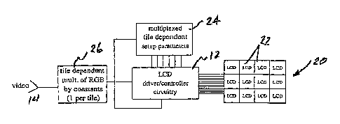
Referring to FIGURE 4, the video signal 14 is now
adjusted (block 26) with a tile-dependent set of constants
(one for each tile 22), in order to match the average tile
brightness for each of the tiles.
Referring to ;ETGURE 5, the discontinuities, or large
level shifts between the edges of each tile 22, are
nullified by making a negative (a graded neutral density
filter having a gradient which is the inverse of the color
CA 02222031 1997-11-24
W~ 97/36281 PCT/US97/04869
11
non-uniformities) 28 of display 20, and placing it over
the screen (not shown) of the display 20. This negative
28 can also be printed on the screen's front polarizes
(not shown), or a separate thin plastic sheet (not shown).
This will match the brightness levels across the entire
surface of the display 20. The exposure will be made so
that the dimmest region has no reduction. only the
brighter regions will be reduced. It is also possible to
accomplish this electronically with another level of tile-
dependent balancing parameters having a finer mesh
(similar to those of block 26).
Referring now to FIGURE 6, there is shown a block
diagram of an alternate method for applying tile-dependent
correction constants to each of a plurality of tiles in a
flat-panel display. A video signal 30 is applied to a
commercially available LCD controller 32. An output
signal 34 from LCD controller 32 is applied simultaneously
to each of a plurality of drivers 36, with each driver 36
being associated with an individual display panel 38.
Each driver 36 is adapted to receive individual correction
constants from parameters 40, which were previously stored
in a memory device (not shown). Alternatively, set-up
parameters may be permanently connected to the driver
circuitry for each tile. In such case, a common
controller can still be used, as illustrated in FIGURE 6.
Individual, predetermined correction constants 40 are
permanently provided to individual tile drivers 36 in this
' arrangement.
Referring now to FIGURE 7, there is shown generally
at reference number 50, a cross-sectional view of the
CA 02222031 2001-06-27
12
structure of a typical, tiled, flat-panel display, used in
the preferred embodiment. It should be understood,
however, that components can be disposed in other
sequences without c9eparting from the scope of this
invention. A color-balancing neutral density filter 52 is
disposed at the top of the display structure 50.
Immediately below :Filter layer 52 is a top optics
layer 59~. This optics layer 54 may contain a mask,
screen, micro-lens or polarizes components, as described
in the aforementioned, U.S. patent. 5,661,531.
Disposed below the optics layer 54
is an optional, color-correcting neutral density
filter 52'. Color-correcting filter 52' could replace
color-balancing filter 52 or could be employed in addition
thereto.. Beneath the optional color-correcting filter 52'
is a plurality of individual tiles 56. In the preferred
embodiment, tiles 56 are AMLCD tiles, with or without top
and/or bottom polarizers.
Directly below tiles 56 is a third color-correcting
neutral density filter 52 " , also optional. As indicated
with filters 52 and 52', color-correcting filter 52 "
could either replace or augment any combination of filters
52 and !52'. Below the optional filter 52 " is a bottom
optics :layer 58. This bottom optics layer 58 may contain
a mask, screen, micro-lens or polarizes components, as
also de:>cribed in ~3etail in U.S. patents 5,661,531 and
5,889,5E~8. The bottom layer of the flat-panel display 50
is a light source 60.
Referring now t:o FIGURE 8, there is shown generally at
CA 02222031 1997-11-24
WO 97/3628i PCT/US97/04869
13
reference number 70 a cross-sectional view of another
embodiment of a tiled, flat-parnel display. This
embodiment differs from the tiled, flat-panel display 50
(FIGURE 7), in that discrete, color-correcting neutral
density filter layers 52' and/or 52 " are associated with
the respective individual tiles 56. That is, each
individual tile 56 has associated with it a unique filter
layer 52' and/or 52 " . In the tiled, flat-panel
display 50 (FIGURE 7), on the other hand, a single filter
layer 52, 52', or 52 " covers more than one tile 56 and
possibly an entire matrix of tiles.
Referring now to FIGURE 9a, there is shown a plan view
of the top surface of a typical, tiled, flat-panel
display 80. Locations A (82), B (84) and C (86) are
points on the surface of display 80. These points 82, 84
and 86 are defined by x,y coordinates along the indicated
x and y axes.
FIGURE 9b graphically depicts the relative optical
transmission T 88 of a tiled, flat-panel display 80
(FIGURE 9a) under average, white-field drive conditions
at y = C, from x = A to x = B. Two relative transmission
curves 90 and 92 are plotted in dashed and solid lines,
respectively. Transmission curve 90 depicts the actual
relative optical transmission across three uncorrected
tile segments 94, 94' and 94 " that are separated by tile
boundaries 96 and 96', as shown. Particular attention
" should be paid to the abrupt discontinuities which occur
at tile boundaries 96 and 96'. Transmission curve 92
shows a corrected, effectively "flat" transmission across
the three tiles 94, 94' and 94 ". The corrected, flat
CA 02222031 1997-11-24
R'O 97/36281 PCT/US97/04869
14
transmission of curve 92 was achieved by the application
of an appropriately graded, neutral density color-
correction filter (not shown). Such a filter effectively
compensates for relative transmission differences across
individual tiles. The filter's effect becomes pronounced
at the tile boundaries 96 and 96', where the abrupt
discontinuities observed in curve 90 are eliminated.
Referring now to FIGURE 10, there is shown a block
diagram interconnecting the components of a typical LCD
1o display. A video signal (riot shown) is first applied to a
graphics controller 100. This graphics controller 100
retrieves digitized image information from memory (not
shown) and generates both image data 102, and control and
synchronization information 104. Graphics controllers are
commercially available.
Image data signal 102, and the control and
synchronization signal 104 are applied to the inputs of an
LCD controller 106, which is typically implemented as an
application-specific integrated circuit (ASIC). The
function of the LCD controller 106 is to generate
additional timing and control signals that are responsive
to input signals 102 and 104, in order to control the row
driver ICs 108 and column driver ICs 110. In addition,
LCD controller 106 provides signals to other circuitry
necessary for the operation of an LCD-type display.
Reference voltage generator 112 provides a set of voltages
(usually DC) necessary to match the unadjusted relative '
transmission of individual LCD tiles, as shown in curve 90
(FIGURE 9b), to the corrected relative transmission '
curve 92. These reference voltages are typically
CA 02222031 1997-11-24
WO 97/36281 PCT/LTS97/04869
generated by circuits, such as operational amplifiers,
digital-to-analog converters or the like. The level of
these reference voltages may be adjusted with any
additional control circuitry (not shown) required by a
5 specific application. For AMLCDs, row drivers 108 may be
implemented as ICs, and generate gate voltage pulses that
are typically in the 15 - 4o volt range to the gate of
thin film transistors (not shown). Typical ICs suitable
for use as column drivers are S-MOS SED2743 and Texas
1o Instruments' type 57600 devices. Column drivers 110
generate the voltage signal levels representative of the
input video signal (not shown). These voltages are
provided to the sub-pixels by gate pulses. Column drivers
110 are generally implemented as ICs, with typical
15 examples being Cirrus Logic CL-FP6522, Texas Instruments
TMS 57481 and Vivid Semiconductor VS1192 devices.
It should be understood that other or ancillary control
and video signal processing-circuitry can be used,
depending on the type of tiles used to construct the flat-
panel display.
Since other modifications and changes varied to fit
particular operating requirements and environments will be
apparent to those skilled in the art, the invention is not
considered limited to the example chosen for purposes of
disclosure, and covers all changes and modifications which
do not constitute departures from the true spirit and
scope of this invention.
CA 02222031 1997-11-24
WO 97/36281 PCT/L1S97/04869
16
Having thus described the invention, what is desired to
be protected by Letters Patent is presented in the
subsequently appended claims.
What is claimed is: