Language selection

Search

Patent 2222319 Summary

Third-party information liability

Some of the information on this Web page has been provided by external sources. The Government of Canada is not responsible for the accuracy, reliability or currency of the information supplied by external sources. Users wishing to rely upon this information should consult directly with the source of the information. Content provided by external sources is not subject to official languages, privacy and accessibility requirements.

Claims and Abstract availability

Any discrepancies in the text and image of the Claims and Abstract are due to differing posting times. Text of the Claims and Abstract are posted:

  • At the time the application is open to public inspection;
  • At the time of issue of the patent (grant).
(12) Patent Application: (11) CA 2222319
(54) English Title: A METHOD AND AN ARRANGEMENT FOR MOUNTING A COMPONENT ON A CARRIER
(54) French Title: METHODE ET DISPOSITIF DE MONTAGE D'UN COMPOSANT SUR UN SUPPORT
Status: Deemed Abandoned and Beyond the Period of Reinstatement - Pending Response to Notice of Disregarded Communication
Bibliographic Data
(51) International Patent Classification (IPC):
  • H05K 03/32 (2006.01)
  • H05K 01/18 (2006.01)
  • H05K 03/30 (2006.01)
  • H05K 03/36 (2006.01)
  • H05K 13/04 (2006.01)
(72) Inventors :
  • HELLGREN, EVA (Sweden)
  • ERIKSSON, MATS (Sweden)
(73) Owners :
  • TELEFONAKTIEBOLAGET LM ERICSSON (PUBL)
  • TELEFONAKTIEBOLAGET LM ERICSSON
(71) Applicants :
  • TELEFONAKTIEBOLAGET LM ERICSSON (PUBL) (Sweden)
  • TELEFONAKTIEBOLAGET LM ERICSSON (Sweden)
(74) Agent: MARKS & CLERK
(74) Associate agent:
(45) Issued:
(22) Filed Date: 1997-11-25
(41) Open to Public Inspection: 1998-05-26
Examination requested: 2002-11-15
Availability of licence: N/A
Dedicated to the Public: N/A
(25) Language of filing: English

Patent Cooperation Treaty (PCT): No

(30) Application Priority Data:
Application No. Country/Territory Date
9604345-0 (Sweden) 1996-11-26

Abstracts

English Abstract


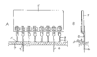
There is a trend in the electronics industry towards
a preference for components that can be surface mounted on a
carrier, such as a circuit board. By using surface mountable
leads on a component together with a "Single-In-Line" technique
it is possible to surface mount a component (5) upstanding on a
circuit board (7) with the component leads surface mounted on
the board. The leads (8) may be bent at their bottom
extremities and provided with feet (10) for effective contact
with the board. Guide and support pins may be used to hold the
component in position during mounting and connecting the
component and to brace the leads on the component when mounted
on the board.


French Abstract

L'industrie électronique a tendance à préférer les composants montables en surface sur support, par exemple une carte de circuit. En utilisant des conducteurs montables en surface sur un composant conjointement avec une technique de montage à une seule rangée de connexions, il est possible de monter en surface un composant (5) debout sur une carte de circuit (7), ses conducteurs étant montés en surface sur la carte. Les conducteurs (8) peuvent être pliés à leurs extrémités inférieures et dotés de pattes (10) assurant un contact efficace avec la carte. Des broches-guides et des broches de soutien peuvent servir à tenir le composant en place pendant le montage et la connexion du composant et à assujettir les conducteurs sur le composant lors du montage sur la carte.

Claims

Note: Claims are shown in the official language in which they were submitted.


CLAIMS
1. A method of mounting a component upstanding on a carrier,
characterized by providing the component with leads of which at
least one is formed into a guide and support pin for guiding
and supporting the component when mounting said component on
said carrier, and connecting the remaining leads.
2. A method according to Claim 1, characterized by bending the
ends of said leads for contact with the carrier, prior to
making said connections.
3 A method according to Claim 1, characterized by cutting-off
the contact leads for direct contact with the carrier with
straight leads, prior to making said connections.
4 An arrangement for surface mounting a component upstanding
on a carrier, characterized in that leads (2) are connected to
the component (5), wherein at least one lead is adapted to form
a guide and support pin (6) and the remaining leads function as
contact leads for connection to the electrical contact points
of the component (4), and wherein when mounting the component on
the carrier (7), the guide and support pin is inserted into a
hole (9) in the carrier and electric leads are connected to
respective contact points on the carrier.
5. An arrangement according to Claim 4, characterized in that
when the contact points and guide hole lie in line on the
carrier, or circuit board, (7), said guide and support pins (6)
are angled.

6. An arrangement according to Claim 4, characterized in that
said guide and support pins (6) are connectable with a band.
7. An arrangement according to Claim 4, characterized in that
the ends of the contact leads (8) are bent so as to provide
better connection with the circuit board (7).
8. An arrangement according to Claim 7, characterized in that
the contact lead ends (10) are J-shaped.
9. An arrangement according to Claim 7, characterized in that
the contact lead ends (10) are gull-wing shaped
10 An arrangement according to any one of Claims 7 to 9,
characterized in that the contact lead ends face in mutually
different directions.
11. An arrangement according to Claim 4, characterized in that
the contact leads are cut so as to be straight for direct
connection.
12. An arrangement according to Claims 4 to 11, characterized
in that prior to mounting, the contact leads (8) and guide and
support pins (6) consist of leads (2) on a lead frame (1).

Description

Note: Descriptions are shown in the official language in which they were submitted.


CA 02222319 1997-11-2~
A METHOD AND AN ARRANGEMENT FOR MOu..ll~G A COMPONENT ON A
~ARRT~R~
FIELD OF INVEN~ION
The present invention relates to a method of surface mounting
an upstanding component on a carrier, and also to an
arrangement for surface mounting an upstanding component on a
carrler.
DESCRIPTION OF THE PRIOR ART
Present day components that are intended to be mounted
upstanding on a circuit board for instance often have straight
leads for insertion into holes such as to affix the component
on the board and to establish an electric contact between
component and board. The leads may be disposed in a Single-In
Line formation (SIL formation). In mounting such a component on
a circuit board, the leads are inserted into metallized holes
provided in the board and the component is held firmly in the
holes through the interaction of the leads, an electrical
connection being established in the holes so as to obtain the
requisite electrical contact between component leads and
circuit board.
SU~5ARY OF THE lNV~iN-LlON
There is a trend in the electronics industry toward the
preference for surface mountable components that can be mounted
on such carriers as circuit boards. Components of this nature
take up less space on a circuit board as seen totally, since it
obviates the need to provide a large number of holes for

CA 02222319 1997-11-2~
instance. Such holes may make the drawing of conductors in
underlying layers difficult to achieve. Furthermore, it is
possible to rationalise circuit board production processes when
solely surface mounted components can be used. Because hole
mounting processes and wave soldering processes can be
dispensed with, production is both simpler and less costly.
By using surface mountable leads on a component in conjunction
with a "Single-In-Line" technique, wherewith the leads may be
bent at their bottom extremities and provided with feet for
contact with the circuit board, and wherewith guide/support
pins are used to hold the component mechanically in place
during the process of mounting and connecting the component and
to brace the leads on the finished board, it is possible to
mount an upstanding component on a circuit board with the
component leads surface mounted on the board.
The surface mounted contact leads may be produced from existing
lead frames or specially adapted contact leads. The leads may
be bent to an appropriate shape with the aid of tools for
forming feet on the respective leads, such that the leads will
be connected effectively to board connection surfaces and be
independent of the position taken by the component when
mounted.
The guide and support pins will preferably be two or more in
number and may be straight or slightly curved, but will always
be longer than the connecting leads so that they can be
inserted into guide holes in the circuit board. The guide and
support pins enable the component to be mounted without the aid
of loose fixtures. The use of a guide and support pin with few

CA 02222319 1997-11-2~
leads is also conceivable, depending on the field of use and
the size of the component concerned.
BRIEF DESCRIPTION OF THE DRAWINGS
Figures lA and B are separate views of a component mounted on a
lead frame.
Figures 2A,B illustrate the component of Fig. 1 with the leads
removed from the lead frame and formed as contact leads and
guide and support pins in accordance with the invention.
Figures 3A and 3B are views which show the component of Fig 2
mounted on and connected to a circuit board.
Figures 4A and B show alternative embodiments of the guide and
support pins.
Figures 5A,-B and cshow alternative embodiments of the contact
leads.
DETAILED DESCRIPTION OF PREFERRED EMBODIMENTS
Seen totally, surface mounted components utilize less space
than hole mounted components, since the surface of an
underlying circuit board layer can be better used for circuit
drawing. When greater possibility of surface mounting
components is found in the production of circuit boards, there
is also found potential for rationalising production since all
components can then be surface mounted and processes relating
to hole-mounting and wave-soldering can be dispensed with in
the manufacturing line.

CA 02222319 1997-11-2~
With a starting point from, e.g., rolled strip material that
comprises essentially several longitudinally combined lead
frame material (see Fig. 1) each individual contact point 3 of
the contact leads 2 in the lead frame 1 is first connected to a
respective contact surface 4 on the component 5 subsequent to
having removed any non-functional lead. The contact points 3 on
the contact leads 2 of the lead frame can be soldered firmly to
respective contact points 4 of the component. Individual
components 5 are removed from the frame-connected components
and tested, see fig. 2, e.g. clipped therefrom. This can be
done in part immediately prior to or during the packing
process, depending on the packing process applied. By allowing
at least one lead to constitute a guide and support pin 6
adapted for hole-mounting in a circuit board 7 with possible
electrical connection to said board, remaining leads can be
used as electric contact leads 8 between component and board.
Existing lead frames can thus be used for components that are
to be surface mounted. Alternatively, contact leads and guide
and support pins can be applied externally directly to the
component for connection therewith. For the purpose of holding
the components in place on a carrier, there are conveniently
used two guide pins 6 which may have been formed from a lead
that would normally have been clipped off. The guide pins may
be straight or slightly curved or angled as shown at 6',see
Fig. 4A, where the contact points and guide holes are in line
on the carrier, for instance. In certain cases, it may be
suitable to place the component upstanding directly on the
carrier and therewith use shortened contact leads and guide-
support pins, see Fig. 4B.

CA 02222319 1997-11-2~
Guide-and-support pin receiving holes 9 have been drilled in
the circuit board 7 to facilitate mounting of components 5 on
said board, said pins and holes functioning to guide and
support the components in thelr intended positions on the
board. The holes 9 in the circuit board will preferably not be
metallised, so as to maintain the correct hole size. The size
of the guide holes may be varied in accordance with lead frames
and the tolerance requirements of the assembly machines used by
a circuit board manufacturer.
Despite the necessity of drilling guide holes in the circuit
board, there is still afforded a saving on the part of the
circuit board manufacturer, by virtue of the fact that a large
number of holes that would otherwise be needed for hole-
mounting components are not now needed.The provision of guide
holes in circuit boards would not seem to present a
disadvantage, since the boards must always be subjected to a
drilling operation in order to provide via holes for
connections between the various layers of the board.
In addition to the aforesaid method steps of manufacturing
components with contact leads 8 and guide and support pins 6,
there is required equipment for bending the lead ends 10 and a
packaging technique. The ends of the contact leads will
preferably have the J-shape shown in Fig. 3B, 4A and 5A, the
gull-wing shape shown in Fig. 5B and the clipped shape with
straight leads shown in Fig. 5C, for direct connection to the
circuit board. When the component has been mounted on the
circuit board, the outwardly projecting free end of the pin may
be removed or, when desired, bent/angled to ensure positive
connection of the component on the circuit board.

CA 02222319 1997-11-2~
When the ends of the contact leads have the shape of a J, there
will always be sufficient surface contact with the connecting
surface on the circuit board with which an electric contact can
be made. Furthermore, there can be obtained a joint 11 which
will have precisely the same amount of connecting material
around the joint even if the component leans to one side or the
other. The guide pins can be left completely straight or may be
bent slightly so as to lie in line with the centre of the J-
bend. An alternative to the J-shape is one in which the J-bends
are in mirror image with one another, as shown in Fig. 5A,
which would also contribute towards obtaining a more stable
placement of the component on the circuit board. Similar
mirror-image configurations that contribute towards enhancing
the stability of the component are also conceivable, e.g.
mirror-image gull wing shapes and other similar shapes of the
lead ends.
When packaging finished components with connected leads and
guide and support pins, the pins, which are longer than the
contact leads, can be used as contact surfaces for adhesive
transporting tape, and the finished components wound up on a
transport reel and then transported to the user.

Representative Drawing
A single figure which represents the drawing illustrating the invention.
Administrative Status

2024-08-01:As part of the Next Generation Patents (NGP) transition, the Canadian Patents Database (CPD) now contains a more detailed Event History, which replicates the Event Log of our new back-office solution.

Please note that "Inactive:" events refers to events no longer in use in our new back-office solution.

For a clearer understanding of the status of the application/patent presented on this page, the site Disclaimer , as well as the definitions for Patent , Event History , Maintenance Fee  and Payment History  should be consulted.

Event History

Description Date
Inactive: IPC from MCD 2006-03-12
Application Not Reinstated by Deadline 2004-11-25
Time Limit for Reversal Expired 2004-11-25
Deemed Abandoned - Failure to Respond to Maintenance Fee Notice 2003-11-25
Letter Sent 2002-12-18
Request for Examination Received 2002-11-15
All Requirements for Examination Determined Compliant 2002-11-15
Request for Examination Requirements Determined Compliant 2002-11-15
Application Published (Open to Public Inspection) 1998-05-26
Inactive: Single transfer 1998-04-27
Inactive: First IPC assigned 1998-04-01
Inactive: IPC assigned 1998-04-01
Classification Modified 1998-04-01
Inactive: IPC assigned 1998-04-01
Inactive: Courtesy letter - Evidence 1998-02-24
Filing Requirements Determined Compliant 1998-02-18
Inactive: Filing certificate - No RFE (English) 1998-02-18
Application Received - Regular National 1998-02-17

Abandonment History

Abandonment Date Reason Reinstatement Date
2003-11-25

Maintenance Fee

The last payment was received on 2002-11-18

Note : If the full payment has not been received on or before the date indicated, a further fee may be required which may be one of the following

  • the reinstatement fee;
  • the late payment fee; or
  • additional fee to reverse deemed expiry.

Patent fees are adjusted on the 1st of January every year. The amounts above are the current amounts if received by December 31 of the current year.
Please refer to the CIPO Patent Fees web page to see all current fee amounts.

Fee History

Fee Type Anniversary Year Due Date Paid Date
Application fee - standard 1997-11-25
Registration of a document 1998-04-27
MF (application, 2nd anniv.) - standard 02 1999-11-25 1999-11-15
MF (application, 3rd anniv.) - standard 03 2000-11-27 2000-11-14
MF (application, 4th anniv.) - standard 04 2001-11-26 2001-11-09
Request for examination - standard 2002-11-15
MF (application, 5th anniv.) - standard 05 2002-11-25 2002-11-18
Owners on Record

Note: Records showing the ownership history in alphabetical order.

Current Owners on Record
TELEFONAKTIEBOLAGET LM ERICSSON (PUBL)
TELEFONAKTIEBOLAGET LM ERICSSON
Past Owners on Record
EVA HELLGREN
MATS ERIKSSON
Past Owners that do not appear in the "Owners on Record" listing will appear in other documentation within the application.
Documents

To view selected files, please enter reCAPTCHA code :


To view images, click a link in the Document Description column. To download the documents, select one or more checkboxes in the first column and then click the "Download Selected in PDF format (Zip Archive)" or the "Download Selected as Single PDF" button.

List of published and non-published patent-specific documents on the CPD .

If you have any difficulty accessing content, you can call the Client Service Centre at 1-866-997-1936 or send them an e-mail at CIPO Client Service Centre.


Document
Description 
Date
(yyyy-mm-dd) 
Number of pages   Size of Image (KB) 
Representative drawing 1998-05-31 1 7
Abstract 1997-11-24 1 19
Description 1997-11-24 6 233
Claims 1997-11-24 2 61
Drawings 1997-11-24 2 36
Filing Certificate (English) 1998-02-17 1 165
Courtesy - Certificate of registration (related document(s)) 1998-07-15 1 140
Reminder of maintenance fee due 1999-07-26 1 114
Reminder - Request for Examination 2002-07-28 1 127
Acknowledgement of Request for Examination 2002-12-17 1 174
Courtesy - Abandonment Letter (Maintenance Fee) 2004-01-19 1 176
Correspondence 1998-02-23 1 30