Note: Descriptions are shown in the official language in which they were submitted.
CA 02222857 1997-12-19
PROCESS TO CREATE METALLIC STAND-OFFS ON AN ELECTRONIC CIRCUIT
The present invention relates to a process to create at least one
stand-off on an electronic circuit.
Although not exclusively reserved therefore, this process is more
particularly applicable to the known "flip chip" technology wherein several
high density electronic chips are assembled onto a printed circuit board
by means of so-called "stand-off's". A stand-off is a metallic stud or bump
which, additionally to interconnecting the chip to the board, creates a
distance between them. This distance is necessary to reduce fatigue effects
in the interconnection due to differences in temperature expansion
coefficients of the chip, generally constituted by silicon, and the carrier;
i.e. the printed circuit board. The stud may obviously not collapse,
especially during the assembly process.
Processes to create stand-offs or studs on a chip are already
known in the art, e.g. from an IBM'" technology called "Controlled
Collapsed Chip Connection" or "C4" technology. Therein, the studs ore
made using evaporation techniques through molybdenum masks. This
known technology involves relatively expensive silicon back-end
processing and, additionally, requires high cost mask material. A method
for electrically connecting flip chips to a printed circuit substrate is for
instance disclosed in the US Patent No. 5,261,593 of Nov. 16, 1993, and
an apparatus therefore is disclosed in the US Patent No. 5,349,500 of
Sep. 20, 1994.
In the known technologies, the stand-offs are realized on the
chips, i.e. by the chip providers. Since several different chips are generally
mounted on a same printed circuit board, the masks for the processing of
these chips need to be created for relatively low production volumes.
Furthermore, at least parts of these "bumping" processes are repeated by
the different chip providers. All these elements lead to increase the
production cost of the flip chip technology.
CA 02222857 1997-12-19
_2_
An object of the present invention is to reduce the number of
operations of the chips and thereby to dramatically reduce the production cost
of a flip chip assembly.
According to the invention, this object is achieved due to the fact
that said stand-off is created on the surface of a printed circuit board
constituting said electronic circuit and being coated with a first layer of
copper, said process including the main successive steps of plating a
second layer of copper at least onto predetermined portions of said first
layer of copper, and of plating a third layer of metal on top of at (east
l0 portions of said second layer of copper.
In this way, the stand-offs are constituted by three layers of
metal located on top of each other on the surface of the printed circuit
board, i.e., in case of the flip chip technology, on the surface of the
carrier rather than on the surface of the chips. The assembly cost is
reduced by the use of only one single back-end processing of the printed
circuit board instead of dealing separately with several chips. In other
words, the cost of the "bumping" process is reduced by staying
independent of the different bumping technologies associated to different
chips. Moreover, the fabrication of "non-melting" stand-offs, i.e.
consisting of metals that are not melting during reflow soldering, gives a
good control of the stand-off height between the chip and the printed
circuit board after assembly.
In more detail, said process includes the steps of:
- depositing a first layer of photo-resistive material covering said
first layer of copper;
- creating a first pattern uncovering said first layer of copper at
least at the location of the future stand-off; and
- plating said second layer of copper onto the uncovered portion
of said first layer of copper, said second layer of copper being
substantially thicker than said first layer of copper.
CA 02222857 1997-12-19
-3-
Stand-offs constituted by two layers of copper are thereby
created on the surface of the printed circuit board. However, for some
applications the height of these stand-offs is not sufficient for create the
above mentioned stand-off.
To this end, the process of the present invention can further be
achieved by using either an electro-plating or an electrochemical-plating
technique.
On the one hand, in case of using the electro-plating, also
called galvano-plating, technique, the present process is further carried
out by including the steps of:
- depositing a second layer of photo-resistive material;
- creating a second pattern uncovering said second layer of
copper at least at the location of said future stand-off; and
- plating said third layer of metal onto the uncovered portion of
said second layer of copper.
In this way, relatively high metallic stand-offs constituted by
three successive layers of copper are created.
The present electro-plating process may be completed by further
including the steps of:
- coating said third layer of metal with a protective layer of
second metal;
- stripping said first and second layers of photo-resistive
material;
- etching the unprotected layers of metal until the unprotected
first layer of copper is removed; and
- stripping said protective layer of second metal.
Due to the relatively higher thickness of the second layer of
copper with respect to that of the first layer of copper, the last etching
step, which is a so-called differential etching step, removes the whole
unprotected portions of the first layer of copper, while it only slightly
affect
the thickness of the unprotected portions of the second layer of copper.
CA 02222857 1997-12-19
-4-
It is further to be noted that the metal of said third layer is
preferably copper.
Finally, the present process may be completed by further including
the step of electrochemical plating a layer of nickel onto the unprotected
layers of copper, and the step of flash plating a layer of gold onto said
layer of nickel.
On the other hand, in case of using the electrochemical-plating
technique, the above process of the present invention is further carried out
by including the steps of:
- coating said second layer of copper with a protective layer of
second metal;
- stripping said first layer of photo-resistive material;
- etching the unprotected first layer of copper;
- stripping said protective layer of second metal,
- depositing a layer of photo sensitive dielectric material;
- creating a second pattern removing said layer of photo
sensitive dielectric material at the location of said future metallic stand-
off;
and
- plating a third layer of metal onto the uncovered portions of
said second layer of copper.
In this way, a relatively high metallic stand-off constituted- by
three successive layers of metal is created.
In a first embodiment of the present electrochemical-plating
process, the metal of said third layer is copper.
The process then further includes the steps of electrochemical
plating a layer of nickel onto said stand-off using said layer of photo
sensitive dielectric material as mask.
In a second embodiment of the present electrochemical-plating
process, the metal of said third layer is nickel.
CA 02222857 1997-12-19
-5-
The electrochemical-plating process is then completed by further
including the step of flash plating a layer of gold onto said layer of nickel
using said layer of photo sensitive dielectric material as mask.
A good electric contact terminal or pad is thereby realized.
In the above processes, the second metal of said protective layer
is preferably tin-lead.
The present technology can be applied to very large area
substrates, i.e. different dimensions of printed circuit boards, combining
several different flip chip Input/output (I/O) locations in one design and
manufacturing process. It further can accommodate the assembly of most
standard available chips.
The above mentioned and other objects and features of the
invention will become more apparent and the invention itself will be best
understood by referring to the following description of an embodiment
taken in conjunction with the accompanying drawings wherein:
Fig's. 1 to 3 show common steps for the electro-plating and the
electrochemical-plating process according to the invention;
Fig's. 4 to 6 show further steps of the electro-plating process;
and
Fig's. 7 to 10 show further steps of the electrochemical-plating
process.
The process show in the drawings Fig's 1 to 10 is used to create
metallic bumps or stand-offs on the surface of a printed circuit board in
order to realize a flip chip assembly.
The drawings show a portion of a transversal section of a
printed circuit board PCB provided with a hole. The board PCB is coated
on its upper and lower surface with a basis layer of copper Cul as shown
in Fig. 1. The processing steps described below lead to obtain, on the
board PCB, an optimal combination of conductive copper paths, elevated
stand-offs and plated-through holes, the stand-offs being used to allow
CA 02222857 1997-12-19
-6-
external Input/output (I/O) connections to flip chips and are also called
"StUdS" .
In the following part of the description, two possible techniques
used to create a metallic stand-off and a plated-through hole will be
explained. The successive processing steps according to a first technique,
called electro- or galvano-plating technique, are represented in the
Fig's 1 to 6, whilst the successive processing steps according to a second
technique, called electrochemical-plating technique, are represented in
the Fig's 1 to 3 and 7 to 10. The Fig's 1 to 3 are thus common for these
two techniques and will be explained only once below.
The first step of the present process consists in depositing a first
layer of photo-resistive material PR1 covering the basis layer of copper
Cul on both sides of the PCB. A pattern is then created in the photo-
resistive material PRl according to a technique well known in the art and
therefore not explained in more detail hereafter. Fig. 2 shows the board
after the creation of the pattern on the layer PR1 .
A further step of the process consists in plating a second layer of
copper Cu2 onto the uncovered portions of the basis or first layer of
copper Cul , i.e. by using the patterned layer PR1 as mask. The second
layer of copper Cu2 has a thickness which is substantially larger than that
of the first layer of copper Cul. This second layer of copper Cu2 is not
only deposited onto the uncovered portions of Cul but also in the hole
drilled through the printed circuit board PCB as shown in Fig. 3.
The above mentioned two techniques differentiate now. The
following explanations relate to the electro-plating or galvano-plating
technique, and the electrochemical-plating technique will be explained
later starting from this step.
In the electro-plating technique, the next step consists in
depositing a second layer of photo-resistive material PR2 on the device as
shown in Fig. 3. A pattern is then create on the second photo-resistive
layer PR2 leaving uncovered the portions of copper Cu2 at the location of
CA 02222857 1997-12-19
_7-
the future stand-off. A further step of this process consists in plating a
third layer of copper Cu3 on these uncovered portions of Cu2. Still by
using the second patterned layer PR2 as mask, a protective metallic layer
of tin-lead SnPb is deposited on top of the layer Cu3. The result is shown
in Fig. 4.
The two layers PR1 and PR2 of photo-resistive material are then
stripped away. Afterwards, the unprotected portions of the layers of
copper Cul and Cu3 are etched until the uncovered portions of the layer
Cul are removed from the board PCB as shown in Fig. 5.
After this differential etching of the copper layers Cul and Cu2
using the tin-lead layer SnPb as mask, the remaining overall thickness of
the two layers of copper Cul and Cu2 is of about 35 tam.
Finally the protective metallic layer of tin-lead SnPb is stripped
away and a high stand-off comprising the three successive layers of
copper Cul, Cu2 and Cu3 is created as shown in Fig. 6. The height of the
metallic stand-off is between 50 and 75 <<m.
The still unprotected layers of copper Cu2 and Cu3 may then be
coated by a relatively thin protective layer of nickel electrochemically
plated thereon. A good electric contact may further be achieved by flash
plating a layer of gold on top of the protective layer of nickel. The result
of these last plating steps are not shown in the figures.
This completes the electro-plating technique.
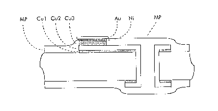
In the electrochemical-plating technique, the step following the
one shown in Fig. 3 is represented in Fig. 7 and consists in depositing a
protective metallic layer of tin-lead SnPb on top of the layer Cu2, using
the patterned photo-resistive layer PR1 as mask. The protective layer SnPb
is deposited in a galvanic way as known in the art.
The photo-resistive layer PR1 is then stripped away and the
remaining uncovered portions of the basis layer of copper Cul are etched
using the layer SnPb as a mask. The result is shown in Fig. 8.
' CA 02222857 1997-12-19
-$_
The following step consists in stripping the protective metallic
layer SnPb. A layer of photo sensitive dielectric material MP is then
deposited over the whole device as shown in Fig. 9. Such a deposition
may for instance be realized by means of the known 'curtain coating"
technique and the dielectric layer MP is for instance constituted by the so-
called "multiposit"'" material of the company "Shipley". The reason of
depositing a layer of photo sensitive dielectric material MP rather than a
photo-resistive layer is that the latter does not resist to a nickel-gold
deposition as will be performed later.
A pattern is then created in the dielectric layer MP as shown in
Fig. 9. This pattern defines the position of the stand-off in a photo-
lithographic way by removing the layer of photo sensitive dielectric
material MP at the location of this future stand-off.
According to a first variant of realization, a third layer of copper
Cu3 is plated onto the then uncovered portions of the second layer of
copper Cu2. A high stand-off comprising the three successive layers of
copper Cul, Cu2 and Cu3 is so created.
As for the above described galvano-plating technique, the third
layer of copper Cu3 may then be coated by a relatively thin protective
layer of nickel Ni electrochemically plated thereon. This plating process
uses the dielectric layer MP as a mask. The process is completed with a
flash deposition or plating of gold Au over the nickel layer Ni. Here again
the dielectric layer MP is used as a mask. The thickness of the gold layer
Au is of about 0.1 t.tm and is used to improve the electric contact with the
chip to be connected to the stand-off.
According to another variant of realization, not shown in the
figures, a relatively thick layer of nickel is plated onto the uncovered
portions of the second layer of copper Cu2. The so-created stand-off is
then constituted by two layers of copper Cul and Cu2 and a thick layer of
nickel. Here again the layer of nickel may be covered by a layer of gold to
provide a good electric contact. It is to be noted that the layers of nickel
' CA 02222857 1997-12-19
-9-
and gold are deposited by using the dielectric layer MP as a mask and
that the gold layer is preferably deposited according to the flash plating
technique.
White the principles of the invention have been described above
in connection with specific apparatus, it is to be clearly understood that
this description is made only by way of example and not as a limitation on
the scope of the invention.