Note: Descriptions are shown in the official language in which they were submitted.
CA 02223068 1997-12-01
TITLE OF THE INV--NTI ON
POWER CONVERTER
BACKGROUND OF T~:_ INVENTION
1. Field of tr.e Invention
This invent on relates to power converters, and more
particularly, to high voltage, large capacity power
converters which connect in series multiple self-turn-off
switching devices.
2. Description of the Related Art
In recent years, power converters which can supply high
voltages and large currents have been desired. In
particular, the ability to supply 2000 ~ 3000A or more at 100
~ 500KV is required by DC transmission and the like.
Fig. 1 is an example of the composition of a prior art
power converter f3r high-voltage and large current.
In Fig. 1, A~ power source 1 is connected to converter 3
via transformer 2. Converter 3 is composed by bridge-
connected switch units 21 ~ 26. Switch unit 21 is composedof self-turn-off switching devices which are bridge-
connected. Here, an example of the case of composition using
gate turn-off thyristors (hereafter, simply "GTO") is
described. DC reactor 4 smooths the DC output current of
CA 02223068 1997-12-01
converter 3. The DC output of converter 3 ls connected to DC
circuit load 5 via DC reactor 4.
Switch unit 21 is composed of GTO 6, GTO 7, dlode 8,
diode 9 and capacitor 11. Since switch units 22 ~ 26 are of
the same composition as switch unit 21, their descriptions
are omitted. Converter 3 converts AC power and DC power
between AC power source 1 and DC circuit 5 bidirectionally
by a 3-phase bridge composed of switch units 21 ~ 26.
In this example, an arm consists of one switch unit.
However, arms may be formed by executing an appropriate
number of parallel connected switch units, DC connections or
the like.
Next, in Fig. 2, the operation of switch unit 21 is
described.
In Fig. 2(a), unit 21 is in the conducting (ON) state.
The current is divided into parallel paths; a first path
passing through diode 8 and GTO 6, and a second path passing
through GTO 7 and diode 9. The flow of the current is shown
by the arrows.
Fig. 2(b) shows the state in switch unit 21 immediately
after GTO 6 and GTO 7 have turned OFF. The current flows by
the path of diode 8, capacitor 11 and diode 9, and charges
capacitor 11. When capacitor 11 is charged and the current
CA 02223068 1997-12-01
becomes zero, switch unit 21 will be in the broken (OFF)
state.
In Fig. 2(ci, switch unit 21 is in the above-mentioned
broken (OFF) stat~.
Fig. 2(d) shows the state immediately after GTO 6 and
GTO 7 have turned ON. The current flows by the path of GTO
7, capacitor 11 and GTO 6, and discharges the charge
accumulated in capacitor 11. When capacitor 11 is
discharged, diode 8 and diode 9 turn ON, and the current
becomes in the state shown in Fig. 2(a).
Thereafter, the states in Fig. 2(a) - Fig. 2(d) are
repeated.
With the above type of power converter, there was the
problem that the balance of the two parallel sharing currents
in Fig. 2(a) (that is to say, the current sharing between
each element) could not be maintained due to differences in
dynamic characteristics, such as the switching
characteristics of the GTO and diode circuit-composition
elements, and static characteristics, such as forward
voltage-drop, during transitions such as from the state in
Fig. 2(d) to Fig. 2(a). If the current sharing cannot be
maintained, the current in either of the two GTOs or diodes
is biased, and the loss in that GTO or diode becomes greater.
CA 02223068 1997-12-01
Ultimately, this is due to dependence on the randomness of
the element.
When design ng a power converter, the system must be
designed tzking 'his unbalance into consideration beforehand.
In the end, the ~oorer the utilization factors of the
elements, tne hiaher becomes the cost of the system.
SUMMARY OF THE INVENTION
That being the case, one object of the present invention
is to provide a power converter designed to maintain the
balance of the currents flowing in two parallel circuits when
bridges are composed by self-turn-off switching devices and
diodes.
Another object of the present invention is to provide a
power converter which, as well as balancing the currents
flowing in two parallel circuits, can make the combined
capacitance of the capacitors greater by increasing the
number of capacitors which couple the two parallel circuits,
and can also reduce the inductance capacitance of the circuit
as a whole.
Yet another object of the present invention is to
provide a power converter which, as well as balancing the
currents flowing in two parallel circuits, can, once the
CA 02223068 1997-12-01
currents have been balanced, reduce the inductance part of
the parallel cir~-_its and can reduce the energy loss.
A further c- ect of the present invention is to provide
a power converte~ which, as well as balancing the currents
flowing in two pa-~llel circuits, works on the transient
currents flowing -n the parallel circuits (particularly when
the current is r sing), and, once the currents are balanced,
can reduce the inductance part of the parallel circuits and
can reduce the energy loss.
A still further object of the present invention is, as
well as balancing the current flowing in two parallel
circuits, to provide a low-cost power converter.
The above object of the present invention can be
achieved by providing a power converter fulfilling the
following structural conditions. A first series circuit is
composed by one end of a first reactor being connected to the
cathode of a firs self-turn-off switching device, while the
anode of a first diode is connected to the other end of the
first reactor. A second series circuit is composed by one
end of a second reactor being connected to the cathode of a
second diode, while the anode of a second self-turn-off
switching device is connected to the other end of the second
reactor. A first capacitor is connected between a first
series connection point, formed by the cathode of the first
CA 02223068 1997-12-01
self-turn-off switching device and the one end of the first
reactor, and a s__ond series connection point, formed by the
cathode of the s~_ond diode and the one end of the second
reactor. A seco.~ capacitor is connected between a third
series connectio- point, formed by the anode of the first
diode and the otrer end of the first reactor, and a fourth
series connectior point, formed by the anode of the second
self-turn-off switching device and the other end of the
second reactor.
The arms are composed by connecting multiple switching
units, formed by connecting in common the cathode of the
second self-turn-off switching device and the cathode of the
first diode, and connecting in common the anode of the second
diode and the anode of the first self-turn-off switching
device.
Another object of the present invention can be achieved
by providing a pcwer converter fulfilling the following
structural conditions. A first series circuit is composed by
one end of a firs~ reactor being connected to the cathode of
a first self-turn-off switching device, while one end of a
second reactor is connected to the other end of the first
reactor, and the anode of a first diode is connected to the
other end of the second reactor. A second series circuit is
composed by one end of a third reactor being connected to the
CA 02223068 1997-12-01
cathode of a second diode, while one end of a fourth reactor
is connected to .he other end of the third reactor, and the
anode of a secona self-turn-off switching device is connected
to the other end of the fourth reactor. A first capacitor is
connected betweer. a first series connection point, formed by
the cathode of t:re first self-turn-off switching device and
the one end of t~e first reactor, and a second series
connection point, formed by the cathode of the second diode
and the one end of the third reactor. A second capacitor is
connected between a third series connection point, formed by
the other end of the first reactor and the one end of the
second reactor, and a fourth series connection point, formed
by the other end of the third reactor and the one end of the
fourth reactor. A third capacitor is connected between a
fifth series connection point, formed by the anode of the
first diode and the other end of the second reactor, and a
sixth series conrection point, formed by the anode of the
second self-turn-off switching device and the other end of
the fourth reactor.
The arms are composed by connecting multiple switching
units, formed by connecting in common the cathode of the
second self-turn-off switching device and the cathode of the
first diode, and connecting in common the anode of the second
CA 02223068 1997-12-01
diode and the ancde of the first self-turn-off switching
device.
Yet another ~bject of the present invention can be
achieved by prov-~ing a power converter fulfilling the
following structu~al conditions. A first series circuit is
composed by one end of the first winding of a reactor having
at least two or ~ore coupled windings being connected to the
cathode of a first self-turn-off switching device, while the
anode of a first diode is connected to the other end of the
first winding of the reactor. A second series circuit is
composed by one end of the second winding of the reactor
being connected to the cathode of a second diode, while the
anode of a second self-turn-off switching device is connected
to the other end of the second winding of the reactor. A
first capacitor is connected between a first series
connection point, formed by the cathode of the first self-
turn-off switching device and the one end of the first
winding of the reactor, and a second series connection point,
formed by the cathode of the second diode and the one end of
the second winding of the reactor. A second capacitor is
connected between a third series connection point, formed by
the anode of the first diode and the other end of the first
winding of the reactor, and a fourth series connection point,
formed by the anode of the second self-turn-off switching
CA 02223068 1997-12-01
device and the other end of the second winding of the
reactor.
The arms ar_ composed by connecting multiple switching
units, formed by sonnecting in common the cathode of the
second self-turn-3~f switching device and the cathode of the
first diode, and _onnecting in common the anode of the second
diode and the an~de of the first self-turn-off switching
device.
BRIEF DESCRIPTION OF THE DRAWINGS
A more complete appreciation of the invention and many
of the attendant advantages thereof will be readily obtained
as the same becomes better understood by reference to the
following detailed description when considered in connection
with the accompanying drawings, wherein:
Figure 1 is ~ prior art power converter;
Figure 2 is ~ drawing showing the operation of a prior
art power converter;
Figure 3 is circuit diagram showing first and second
embodiments of th~ power converter;
Figure 4 is a circuit diagram showing third, fourth and
fifth embodiments of the power converter;
Figure 5 is a circuit diagram showing a sixth embodiment
of the power converter;
CA 02223068 1997-12-01
Figure 6 is a circuit diagram showing a seventh
embodiment of the power converter; and
Figure 7 is _ circuit diagram showing an eighth
embodiment of the power converter.
DETAILED DESCRIP.ION OF THE PREFERRED EMBODIMENTS
Referring n-~ to the drawings, wherein like reference
numerals designate identical or corresponding parts
throughout the several views, and more particularly to Fig. 3
thereof, one embodiment of the present invention will be
described.
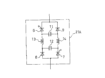
Fig. 3 is a circuit diagram of switch unit 21A which is
this embodiment.
Fig. 3 represents one switch unit. Although a converter
is composed of multiple units as in Fig. 1, since the
composition and o?eration of each switch unit is the same,
then their descri?tions have been omitted.
In Fig. 3, the anode of GTO 7 and the anode of diode 8
are connected. This connection point forms one end of switch
unit 21A in Fig. 3. One end of reactor 13 and one end of
capacitor 12 are connected to the cathode of diode 8. The
other end of capa_itor 12 is connected to the cathode of GTO
7 and one end of reactor 14. The anode of GTO 6 and one end
of capacitor 11 are connected to the other end of reactor 13.
CA 02223068 1997-12-01
The anode of diode 9 and the other end of capacitor 11
are connected tc the other end of reactor 14. The cathode of
GTO 6 and the ca hode of diode 9 are connected. This
connection point forms the other end of switch unit 21A.
In Fig. 3, the current during the ON and OFF of GTOs 6
and 7 flows respectively through reactors 13 and 14. When
that current varies, according to that rate-of-change,
voltages are generated at both ends of reactors 13 and 14.
Normally, because those voltages are of a sufficiently larger
value than the randomness of the forward voltage-drops of the
GTOs and diodes, they act to inhibit the unbalance of the two
parallel currents.
Reactors 13 and 14 also have the effect of inhibiting
the variation of the respective currents which are flowing,
and they act to inhibit the difference in size of the
currents generated by the randomness of the switching
characteristics of GTOs 6 and 7, even though the ON/OFF times
are random(e.g. there is a little bit difference of the
ON/OFF times between GTO 6 and GTO 7 ).
The second embodiment is the case when the inductance
values of the two reactors 13 and 14 in Fig. 3 have been
selected so that they are equal. This embodiment is not
illustrated.
CA 02223068 1997-12-01
Since the basic operation is the same as in the first
embodiment, its description is omitted.
In particul~r, by selecting the inductance values so
that they are just equal, there is no difference in the
impedances of the circuits through which the two parallel
currents pass, and the current sharing is improved.
Fig. 4 shows a third embodiment of a power converter of
this invention. This drawing is a block diagram of switch
unit 21B.
In Fig. 4, one end of reactor 13 is connected to one end
of each of capacitor 12 and reactor 19. One end of reactor
14 is connected to the other end of capacitor 12 and to one
end of reactor 20. The other end of reactor 19 is connected
to one end of capacitor 18 and the cathode of diode 8. The
other end of reactor 20 is connected to the other end of
capacitor 18 and the cathode of GTO 7. Since the composition
thereafter and the basic operation equate to Fig. 3, their
descriptions are omitted.
When using this embodiment, since the voltages generated
at both ends of the reactors are sufficiently larger values
than the randomness of the forward voltage-drops of the GTOs
and diodes, the unbalance of the two parallel currents can be
inhibited.
CA 02223068 1997-12-01
Moreover, compared with the embodiment in Fig. 3, since
the number of capacitors can be increased, the combined
capacitance o~ t:~e capacitors as a whole can be increased.
Since the overal combined capacitance can be increased, the
unbalance of the two parallel currents can be inhibited more
rapidly than wit:~ the embodiment in Fig. 3.
The fourth embodiment is the case when the capacitances
of capacitors 11, 12 and 18 in Fig. 4 have been selected so
that they are equal. This embodiment is not illustrated.
By selecting the capacitances so that they are equal,
when the capacitors are charging and discharging, there is no
difference in the impedances of the circuits through which
the two parallel currents pass, and the current sharing is
improved.
The fifth embodiment is the case when the capacitance of
capacitor 12 ln Fig. 4 is made a greater capacitance value
than the other tw~ capacitors 11 and 18. This embodiment
also is not illustrated.
Since, by this means, the charging currents flowing in
the capacitors become smaller when the capacitors are
charging and discharging, the effect is that unbalance of the
parallel currents flowing in the two GTOs 6 and 7 can be
inhibited.
CA 02223068 1997-12-01
Fig. 5 is a sixth embodiment of the power converter of
this invention. The drawing is a block diagram of switch
unit 21C.
In Fig. 5, ,he cathode of diode 8 is connected to one
end of capacitor 12 and one end of one of the windings of
reactor (transfo-mer) 14. The other end of that one winding
of reactor 14 is connected to one end of capacitor 11 and the
anode of GT0 6.
The cathode of GTO 7 is connected to the other end of
capacitor 12 and one end of the other winding of reactor 14.
The other end of that other winding of reactor 14 is
connected to the other end of capacitor 11 and the anode of
diode 9.
Since the composition thereafter equates to Fig. 3, its
description is omitted. In Fig. 5, the windings of reactor
14 are coupled in the directions shown in the drawing (the
beginnings of the windings are shown by O).
By this coupling, when the parallel currents are flowing
equally in the same direction (for instance, from the bottom
to the top of the drawing), reactor 14 hardly operates.
However, when an unbalance occurs in the parallel
currents, mutual inductance is generated by the coupling
operation of reactor 14, and the unbalanced parts of the
currents are inhibited.
14
CA 02223068 1997-12-01
Fig. 6 is a seventh embodiment of the power converter of
this invention. The drawing is a block diagram of switch
unit 21D.
In Fig. 6, ~'~e cathode of diode 8 is connected to one
end of capacitor 12 and, at the same time, is connected to
one end of capac ~or 11 and the anode of GTO 6 via ferrite
core 16 on which a specified number of turns of copper wire
are wound as the primary side. The cathode of GT0 7 is
connected to the other end of capacitor 12 and, at the same
time, is connected to the other end of capacitor 11 and the
anode of diode 9 via ferrite core 16 on which a specified
number of turns of copper wire are wound as the secondary
side. Since the composition thereafter equates to Fig. 3,
its description is omitted.
By this means also, the operation is to inhibit the
unbalance of the LWo parallel currents in the same way as in
the sixth embodir.ent.
When using this embodiment, ferrite core 16 operates as
a saturable reactor. In particular, since it has B-H curve
characteristics, it only operates during the rising of the
transient current. Therefore, the effect is outstanding when
compared with the embodiment in Fig. 5.
CA 02223068 1997-12-01
Fig. 7 is an elghth embodiment of the power converter of
this invention. The drawing is a block diagram of switch
unit 21E.
In Fig. 7, ~he cathode of diode 8 is connected to one
end of capacitor 12 and, at the same time, is connected to
one end of capacitor 11 and the anode of GTO 6 via closely
coupled parallel bus (conductive bar) 17 in which silicon
steel plates are laminated and around which a specified
number of turns of copper wire are wound as the primary side.
The cathode of GTO 7 is connected to the other end of
capacitor 12 and, at the same time, is connected to the other
end of capacitor 11 and the anode of diode 9 via closely
parallel bus 17 around which a specified number of turns of
copper wire are wound as the secondary side. Since the
composition thereafter equates to Fig. 3, its description is
omitted.
By this means also, the operation is to inhibit the
unbalance of the two parallel currents in the same way as in
the sixth embodiment.
Incidentally, in the various embodiments mentioned
above, the semiconductor elements which compose the power
converters are taken as GTOs. However, this invention is not
limited to GTOs alone, and the same effects can be obtained
even by using other types of self-turn-off switching devices.
CA 02223068 1997-12-01
Also, the above descriptions have taken as examples
power converters _omposed by bridge-connecting arms which are
composed of one ~-.iitch unit. However, with this invention
there are no lim-~s to the number of switch units, and the
same effects can be obtained in the case of composing the
arms by series-ccnnecting multiple switch units or in the
case of composin~ the arms by parallel-connecting multipl~
switch units.
When comparing the embodiments of Fig. 5, Fig. 6 and
Fig. 7, cost-wise the embodiment of Fig. 7 is the cheapest,
and they become dearer in the order of the embodiment of Fig.
6 and the embodiment of Fig. 5.
When using the various embodiments as described above,
the unbalance of the parallel currents which flow in two
self-turn-off switching devices (GTOs) which conduct currents
in parallel can be inhibited. Therefore, the thermal
conditions in each GTO, which are the cause of losses
generated by passing currents, can also be made almost equal.
Also, a power converter with a good utilization factor can be
provided which has no limits to capacitance design etc. of
systems due to the restraints of one side being biased.
Obviously, numerous additional modifications and
variations of the present invention are possible in light of
the above teachings. It is therefore to be understood that
17
CA 02223068 1997-12-01
within the scope of the appended claims, the invention may be
practised otherwise than as specifically described herein.
18