Note: Descriptions are shown in the official language in which they were submitted.
CA 02223341 1997-12-03
TITLE OF THE INVENTION
OPTICAL SWITCH CAPABLE OF DETECTING SWITCHING OPERATION
BACKGROVND OF THE INVENTION
The present invention relates to an optical switch
and, more particularly, to an optical switch having a
technique for confirming whether a switching operation
is correctly performed in the optical switch used to
switch an optical path.
AS is well known, in the optical communication
system, for example, when a plurality of optical lines
each made of an optical fiber are to be tested, test
light must be input to each line by sequentially
switching the lines. In this case, an optical switch
has conventionally been used.
The optical switch used for the above purpose has
a plurality of light guides for inputting/outputting
light, and is constituted such that a specific light
guide can be selectively coupled to another designated
light guide.
FIG. 10 shows the mechanism portion of a conven-
tional optical switch for mechanically changing the
direction of the optical axis of a specific light guide
to switch the optical path.
In this optical switch, the tip of one optical
fiber collimator (prepared by arranging a lens at
the tip of the fiber) 1 constituting the specific
optical guide is rotated by a stepping motor 2 every
CA 02223341 1997-12-03
predetermined angle a.
Remaining optical fiber collimators 31, 32
3n are laid out such that the optical axls of each
optical fiber collimator 3 coincides with the optical
axis of the optical fiber collimator 1 at every
interval of the predetermined angle a.
By supplying, to the stepping motor 2, a pulse
signal necessary for rotating the optical fiber
collimator 1 through an angle N- a (N is an integer),
the optical fiber collimator 1 can be optically coupled
to an arbitrary one of the remaining optical fiber
collimat~rS 31~ 32~ ~ 3n-
In the optical switch using, as a driving source,the stepping motor 2 which rotates through an accurate
rotation angle in accordance with an electrical (pulse)
signal supplied in the above manner, an error may occur
in the stepping motor itself, a circuit for supplying
a driving pulse to the stepping motor, or the like.
In this case, even if the optical axis of the ~
specific optical fiber collimator 1 does not coincide
with that of a desired optical fiber collimator 3, this
cannot be externally known.
When, therefore, this optical switch is used
to test many optical lines, as described above, an
erroneous test may be performed.
Another conceivable method is to detect the
intensity of light passing through the optical fiber
CA 02223341 1997-12-03
collimator.
In this case, however, the light intensity must be
measured at a connection portion between the optical
fiber collimator and the optical line in order to
measure the intensity of test light in a test system of
testing the optical line made of an optical fiber.
For this reason, measurement of the light inten-
sity adversely affects an optical line test.
BRIEF SUMMARY OF THE INVENTION
It is, therefore, an object of the present
invention to provide an optical switch in which the
above-mentioned problems are solved, and an optical
path switching error can be known.
According to the present invention, there is
provided an optical switch comprising a plurality of
light guides for inputting/outputting light, optical
path formation means, having a driving source which
operates upon reception of an electrical slgnal, for
forming an optical path extending from a specific light
guide of the plurality of light guides to arbitrary one
of remaining light guides in order to optically couple
the specific light guide to the one arbitrary light
guide, switching means for supplying, to the driving
source of the optical path formation means, a
predetermined electrical signal for coupling the
specific light guide to the one arbitrary light guide,
and detection means for detecting a formation position
CA 02223341 1997-12-03
of the optical path formed by the optical path
formation means.
Note that the optical path formation position
detected by the detection means is the formation
position of an optical path formed by the optical path
formation means that changes depending on a combination
of the specific light guide and each of the remaining
light guides.
Additional objects and advantages of the invention
will be set forth in the description which follows, and
in part will be obvious from the description, or may be
learned by practice of the invention.
The objects and advantages of the invention may be
realized and obtained by means of the instrumentalities
and combinations particularly pointed out in the
appended claims.
BRIEF DESCRIPTION OF THE SEVERAL VIEWS OF THE DRAWING
The accompanying drawings, which are incorporated
in and constitute a part of the specification,
illustrate presently preferred embodiments of the
invention and, together with the general description
given above and the detailed description of the
preferred embodiments given below, serve to explain the
principles of the invention.
FIG. 1 is a plan view showing the mechanism
portion of an optical switch according to an embodiment
of the present invention;
CA 02223341 1997-12-03
FIG. 2 is a side view showing the mechanism
portion of the optical switch according to the
embodiment of the present invention;
FIG. 3 is an exploded view showing the main part
of the mechanism portion of the optical switch
according to the embodiment of the present invention;
FIG. 4 is a table showing the relationship between
the direction of the optical axis of a specific optical
fiber collimator and an output from a sensor;
FIG. S is a block diagram showing the arrangements
of the optical switch and a measurement system
according to the embodiment of the present invention;
FIG. 6 is a flow chart showing the processing
procedure of the main part of the optical switch
according to the embodiment of the present invention;
FIGS. 7A, 7B, and 7C are views for explaining
the operation of the optical switch according to the
embodiment of the present invention;
FIG. 8 is a schematic view showing the mechanism
portion of an optical switch according to another
embodiment of the present invention;
FIG. 9 is a schematic view showing the mechanism
portion of an optical switch according to still another
embodiment of the present invention; and
FIG. 10 is a schematic view showing the mechanism . :
portion of a conventional optical switch.
CA 02223341 1997-12-03
DETAILED DESCRIPTION OF THE INVENTION
Reference will now be made in detail to the
presently preferred embodiments of the invention as
illustrated in the accompanying drawings, in which like
reference characters designate like or corresponding
parts throughout the several drawings.
The present invention will be generally described.
To achieve the above object, as shown in FIG. 1, an
optical switch of the present invention having a
plurality of light guides (271 - 2712, 36) for
inputting/outputting light, a variable mechanism
(24, 35) which has a driving source (24) that operates
upon reception of an electrical signal, and which
varies the direction or position of at least one
specific light guide of the light guides or an optical
member interposed between the specific light guide and
another light guide in order to optically couple the
specific light guide and another arbitrary light guide,
and a switching means (40) for receiving a signal
designating any one of the remaining light guides, and
supplying an electrical signal corresponding to the
signal, to the driving source of the variable mechanism
to couple the specific light guide to the designated
light guide comprises
a detection means (30, 38, 39) arranged in the
variable mechanism to detect the direction or position
of the specific light guide or the optical member
CA 02223341 1997-12-03
interposed between the specific light guide and another
light guide that is varied by the variable mechanism,
and
a determination means (42) for determining whether
an output from a sensor corresponds to the signal
designating the light guide.
An optical switch according to an embodiment of
the present invention based on the above general
description will be described below with reference to
the several views of the accompanying drawing.
FIGS. 1 to 3 are views showing the mechanism
portion of the optical switch according to the
embodiment of the present invention.
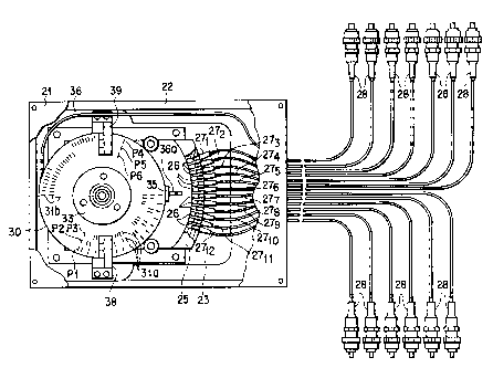
In FIGS. 1 to 3, the mechanism portion of the
optical switch is incorporated in a box-like chassis 22
having upper and lower portions closed with covers 21.
The interior of the chassis 22 is divided into
upper and lower portions by a partition plate 23.
A variable mechanism of this embodiment and a
stepping motor 24 serving as its driving source are
fixed on the lower surface of one end of the partition
plate 23 so as to protrude a rotating shaft 24a to the
upper surface side of the partition plate 23.
The stepping motor 24 is constituted to rotate ltS
rotating shaft 24a at a resolution of, e.g., 0.9~.
A holder 25 stands on the upper surface of the
other end of the partition plate 23.
CA 02223341 1997-12-03
The holder 25 has 12 horizontal support holes 26
centered on an axis C of the rotating shaft 24a of the
stepping motor 24 at an interval of 3.6~.
One end 27a of each of 12 optical fiber collima-
tors 271 to 2712 serving as light guides is fitted in
a corresponding support hole 26 of the holder 25.
An optical connector 28 is attached to the other
end of each of the optical fiber collimators 271 to
2712 extending from the chassis 22.
A slit disk 30 serving as an encoder for present-
ing an optical path formation position corresponding to
the rotation angle is concentrically attached to the
upper portion of the rotating shaft 24a of the stepping
motor 24.
Three arrays P1 to P3 of slits 31a and three
arrays P4 to P6 of slits 31b are formed in two
symmetrical peripheral areas 30a and 30b of the slit
disk (encoder) 30 to detect the angle of the optical
axis of an optical fiber collimator 36 (to be described
later).
While the slit disk (encoder) 30 is fittéd on
the rotating shaft 24a of the stepping motor 24
through a hole 32 formed in the center of the slit
disk 30, the slit disk 30 is screwed to be vertically
sandwiched between two attaching members 33 and 34 as
small-diameter disks, and fixed to the rotating
shaft 24a of the stepping motor 24 together with
CA 02223341 1997-12-03
the attaching members 33 and 34.
A holder 35 is fixed on the lower surface of the
attaching member 34.
The holder 35 horizontally supports one end 36a of
the optical fiber collimator 36 constituting a specific
light guide of this embodiment.
One end 36a of the optical fiber collimator 36 is
supported such that one end 36a is flush with one end
27a of each of the optical fiber collimators 271 to
2712, and the optical axis of the optical fiber
collimator 36 rotates about the axis C of the rotating
shaft 24a of the stepping motor 24.
The optical fiber collimator 36 can be optically
coupled to any one of the remaining optical fiber
collimators 271 to 2712 by rotation of the stepping
motor 24.
The other end of the optical fiber collimator 36
is pulled out outside the chassis 22, and an optical
connector 28 is attached to the tip of the other end,
similar to the optical fiber collimators 271 to 2712.
Sensors 38 and 39 constituting a detection means
of this embodiment together with the slit disk 30 are
arranged at positions symmetrical about the rotating
shaft 24a of the stepping motor 24.
Each of the sensors 38 and 39 is a photolnter-
rupter made up of three pairs of light-transmitting and
light-receiving portions vertically facing each other
CA 02223341 1997-12-03
-- 10
with a gap, and fixed to the partition plate 23 so as
to pass the slit array of the slit disk (encoder) 30
through the gap.
One sensor 38 irradiates light on the slit arrays
P1 to P3 from one surface side of the slit disk 30, and
receives the light passing through the slits 31a in
units of slit arrays to output parallel light-receiving
signals.
The other sensor 39 irradiates light on the slit
arrays P4 to P6 from one surface side of the slit disk
(encoder) 30, and receives the light passing through
the slits 31b in units of slit arrays to output
parallel light-receiving signals.
FIG. 4 shows the relationship between the
direction of the optical axis of the optical fiber
collimator 36 and the light-receiving signals output
parallel from the sensors 38 and 39.
More specifically, in FIG. 4, the least signifi-
cant bit is a light-receiving signal for the slit
array P1, the second bit is a light-receiving signal
for the slit array P2,..., the most significant bit is
a light-receiving signal for the slit array P6, and-the
light-receiving signal is represented by 6-bit data
using [1] as a signal upon receiving light and [0] as
a signal upon receiving no light.
As shown in FIG. 4, when the optical axis of
the optical fiber collimator 36 directs a reference
CA 02223341 1997-12-03
position Ro shifted outward from the optical axis of
the optical fiber collimator 271 to the optical fiber
collimator 271 by 3.6~, parallel data [111111] is
output from the sensors 38 and 39 which detect the
heads of the slits 31a and 31b of the respective slit
arrays Pl to P6.
When the optical axis of the optical fiber
collimator 36 rotates clockwise (in FIG. 1) through
3.6~ from the reference position Ro (the optical axis
of the optical fiber collimator 36 coincides with that
of the optical fiber collimator 271), data [000001] is
obtained.
The data value is set to be incremented by
one every time the optical axis of the optical
lS fiber collimator 36 rotates clockwise through 3.6~.
At an angular position between the slit arrays, the
light-receiving signal data is [000000].
A data value output from the sensors 38 and 39
which detect optical path formation position
information presented by the slit disk (encoder) 30,
except for the data value [oooooo]~ corresponds to .
the number (the suffix of the reference numeral) of
each of the optical fiber collimators 271 to 2712
when the optical fiber collimators 271 to 2712 are
sequentially counted from the one nearest to the
reference position Ro.
FIG. 5 shows the whole arrangement of an optical
CA 02223341 1997-12-03
- 12
switch 20 having the above mechanism portion, and the
configuration of a test system using it.
In FIG. 5, a switching unit 40 of the optical
switch 20 iS constituted by, e.g., a CPU, and receives
a designation signal output from a controller 50 (to be
described later) to output a pulse signal necessary for
coupling the optical fiber collimator 36 to an optical
fiber collimator 27 corresponding to the designation
signal, from a driving pulse output circuit 41 to the
stepping motor 24.
When the switching unit 40 receives a signal
indicating an error from a determination unit 42 ( to be
described later) upon driving the stepping motor 24, it
performs processing such as re-driving of the stepping
motor 24 in accordance with the signal.
The determination unit 42 iS constituted by, e.g.,
a CPU. The determination unit 42 checks whether output
data from the sensors 38 and 39 corresponds to the
designation signal after the switching unit 40 changes
the direction of the optical axis of the optical fiber
collimator 36. If so, the determination unit 42
outputs a signal indicating normal switching to the
switching unit 40; otherwise, the determination unit 42
outputs a signal indicating an error, and the data from
the sensors 38 and 39 to the switching unit 40.
When a test is performed for a plurality of
optical lines each made of an optical fiber by
CA 02223341 1997-12-03
- 13
using the optical switch 20 having this arrangement,
the optical connector 28 of the optical fiber
collimator 36 of the optical switch 20 is connected
to an optical pulse tester (Optical Time Domain
Reflectometer: OTDR) 45. At the same time, the optical
connectors 28 of the optical fiber collimators 271
to 2712 are connected to lines to be tested (not shown).
The controller 50 controls the optical switch 20
and the optical pulse tester 45 to sequentially
and automatically test the lines by using optical
pulses.
The optical pulse tester (OTDR) 45 supplies an
optical pulse to a fiber, and obtains the level of the
light (Fresnel reflected light or back scattering
light) returning from the fiber to its incident end
until a predetermined time elapses after supplying the
optical pulse. From changes in level over time, the
optical pulse tester 45 measures changes in loss of
the fiber, and the presence/absence or position of a
disconnection or the like.
FIG. 6 is a flow chart showing the processing
procedure of the switching unit 40 of the optical
switch 20 used in the above test system.
The operation of the optical switch will be
explained below with reference to FIG. 6.
Assume that the controller 50 inputs a signal N
(= 3) designating the third optical fiber collimator
CA 02223341 1997-12-03
- 14
273 to the optical switch 20 while the optical axis of
the optical fiber collimator 36 directs the reference
position Ro (step S1).
Then, the switching unit 40 calculates an angle A
S (in this case, A = 3 x 3.6~) defined between the
current direction (reference position) of the optical
axis of the optical fiber collimator 36, and a position
where the optical axis of the optical fiber collimator
36 coincides with that of the optical fiber collimator
273 (step S2).
The switching unit 40 causes the driving pulse
output circuit 41 to output, to the stepping motor 24,
pulses corresponding to a number (for example, A/0.9 =
12 when 0.9~-rotation can be attained for one pulse)
required to rotate the optical axis of the optical
fiber collimator 36 through the angle A (step S3).
As shown in FIG. 7A, the stepping motor 24 which
receives the pulses tries to rotate the optical axis of
the optical fiber collimator 36 through the angle A
from the reference position Ro, make the optical axis
of the optical fiber collimator 36 coincide with that
of the third optical fiber collimator 273 designated,
and obtain a predetermined optical path formation
pos ition .
After the switching unit 40 rotates the stepping
motor 24, the determination unit 42 checks whether
6-bit data from the sensors 38 and 39 corresponds to
CA 0222334l l997-l2-03
- 15
the designation signal N (= 3) (in this embodiment,
they correspond to each other).
As shown in FIG. 7A, when the optical axis of the
optical fiber collimator 36 coincides with that of the
third optical fiber collimator 273 designated, data
from the sensors 38 and 39 is tO00011], which coincides
with the designation signal N (= 3). Therefore, the
determination unit 42 determines that the predetermined
optical path formation position is obtained, and
outputs a signal indicating normal switching (step S4).
Upon reception of this signal, the switching
unit 40 stores the designation signal N as data R
representing the current position in a memory (not
shown), outputs a signal indicating switching comple-
tion to the controller 50, and returns to step S1 to
wait for input of a next designation signal (steps SS
and S6).
Assume that an error occurs in the stepping
motor 24, and the sensors 38 and 39 output data
[000010] though the optical axis of the optical fiber
collimator 36 is at a position where it coincides with
the optical axis of the second optical fiber collimator
272, as shown in FIG. 7B.
In addition, assume that the optical axis of the
optical fiber collimator 36 is at a position shifted by,
e.g., 0.9~ from the optical axis of the third optical
fiber collimator 273 designated, and the sensors 38 and
CA 02223341 1997-12-03
- 16
39 output data [000000], as shown in FIG. 7C.
In the case of noncoincidence, the determination
unit 42 determines that the predetermined optical path
formation position cannot be obtained, and outputs a
signal indicating an error, and the data to the
switching unit 40 (step S4).
Upon reception of the data [000000] together with
the signal indicating an error from the determination
unit 42, the switching unit 40 causes the driving pulse
output circuit 41 to output a pulse so as to rotate
the stepping motor 24 every step of 0.9~ over the range
of +2.7~ because the current direction of the optical
fiber collimator 36 is unknown (step S7).
The switching unit 40 checks the determination
result of the determination unit 42 every time a pulse
corresponding to 0.9~ is output. If the determination
unit 42 outputs a signal indicating normal switching,
the flow shifts to step S5 (step S8).
However, when data from the determination unit 42
remains [000000] even upon supplying a pulse corre-
sponding to 2.7~, the switching unit 40 outputs a
signal indicating a switching failure to the controller
50 (steps S7 to S10).
When the switching unit 40 receives data except
for [000000] together with a signal indicating an error
from the determination unit 42 in step S4 or S8, it
calculates an angle B to the reference position Ro
CA 02223341 1997-12-03
- 17
from the data, and causes the driving pulse output
circuit 41 to output a pulse for rotating the stepping
motor 24 through the angle B toward the reference
position Ro (steps Sll and S12).
The switching unit 40 checks the determination
result of the determination unit 42. ~hen the
switching unit 40 receives data [111111] together with
a signal indicating an error from the determination
unit 42, it outputs, to the stepping motor 24, pulses
corresponding to a number required to rotate the
optical axis of the optical fiber collimator 36 to an
angular position corresponding to the designation
signal N, and then checks the determination result of
the determination unit 42 again. If the determination
result indicates normal switching, the flow shifts to
step S5; otherwise, the flow shifts to step S10 to
output a signal indicating switching failure to the
controller 50 (steps S13 to S15).
If the controller 50 receives a signal indicating
switching completion from the optical switch 20 after
outputting the designation signal N to the optical
switch 20, it supplies an optical pulse from the
optical pulse tester 45 to a line to be tested which is
connected via the optical switch 20 to the optical
fiber collimator 273 corresponding to the designation
signal, and obtains changes in level of the llght
returning from the line by using the optical pulse
CA 02223341 1997-12-03
_ 18
tester (OTDR) 45. After the controller 50 makes
the user check an increase in loss of the line or the
presence/absence of a disconnection, the controller 50
outputs, to the optical switch 20, a designation
signal N corresponding to an optical fiber collimator
connected to a next line to be tested, thereby testing
the next line.
If the controller 50 receives a signal indicating
a switching failure from the optical switch 20, it
interrupts the test, and notifies the manager of the
test system of the switching failure. Alternatively,
the controller 50 supplies a designation signal
corresponding to a next line to be tested to the
optical switch 20. When recelving a signal indicating
lS a switching failure from the optical switch 20, the
controller stops the test.
More specifically, the common optical fiber
serving as a specific light guide connected to each of
optical paths serving as a plurality of light guides,
and the slit disk (encoder) having slits representing
optical path data are fixed with a predetermined
positional relationship on the switching driving unit
(stepping motor) of the optical switch according to the
present invention.
The detection means (photointerrupter) for reading
optical path data from the slits of the slit disk
(encoder) is fixed with a predetermined positional
CA 02223341 1997-12-03
-- 19
relationship with the switching driving unit.
The external control unit supplies optical
path data 1 to the stepping motor in order to connect
the common optical fiber to a predetermined optical
path.
Then, the stepping motor operates to move the
common optical fiber and the slit disk (encoder),
thereby connecting the common optical fiber to the
predetermined optical path.
At this time, the photointerrupter detects optical
path data 2 from the slits of the slit disk (encoder).
The switching operation of the optical switch is
determined by comparing optical path data 1 and data 2
with each other.
lS If the switching operation of the optical switch
is normal, the optical path data 1 is identical to
data 2; otherwise, they are not identical.
By determining the switching operation of the
optical switch, therefore, the reliability of the
optical path test can be increased.
In this manner, the optical switch 20 can know
whether the specific optical fiber collimator 36 is
coupled to a designated optical fiber collimator 27.
Erroneous measurement performed when the specific
optical fiber collimator 36 is not coupled to any
optical fiber collimator or is coupled to an optical
fiber collimator different from a designated optical
CA 02223341 1997-12-03
- 20
fiber collimator can be prevented.
When the specific optical fiber collimator 36
cannot be correctly coupled to the designated optical
fiber collimator, they are tried to be coupled again
after the optical axis of the optical fiber collimator
36 is rotated over a predetermined range or temporarily
returned to a reference position and then rotated to be
coupled to the designated optical fiber collimator
again.
Even when, therefore, switching is not correctly
performed occasionally due to a slip of the stepping
motor 24 or the like, an automatic test using this
optical switch need not be suspended. ~-
In the optical switch 20, six slit arrays are
formed for 12 optical fiber collimators 27.
This number is set in consideration of an increase
in the number of optical fiber collimators 27.
More specifically, the number of optical fiber -
collimators 27 can be maximized to 49 ( 180 . 3.6 - 1) at
an interval of 3.6~.
When the number of optical fiber collimators 27 iS
12, as described above, the number of slit arrays may
be decreased to four.
In the above embodiment, the optical axis of the
optical fiber collimator 36 serving as one light guide
is directly rotated by the stepping motor 24.
To the contrary, as shown in FIG. 8, the optical
CA 02223341 1997-12-03
fiber collimator 36 may be constituted such that its
optical axis crosses those of remaining M optical fiber
collimators 271 to 27m at one point on a mirror surface
6la of a reflecting mirror 61 rotated by the stepping
motor 24, and the angle of the reflecting mirror 61 may
be detected by the slit disk (encoder) 30.
In the above embodiment, the optical axis of the
optical fiber collimator 36 serving as a specific light
guide is rotated.
In contrast, as shown in FIG. 9, the optical fiber
collimators 271 to 27m may be aligned in one straight
line at a predetermined interval, the optical fiber
collimator 36 may be constituted to be moved parallel
to the alignment direction of the optical fiber
collimators 271 to 27m together with a band-like slit
plate (encoder) 71 by a variable mechanism 73 having
the stepping motor 24 as a driving source, and slits 72
of the slit plate 71 may be detected by the sensors 38
and 39.
In addition to the method using slits for
shielding and passing through light, as in the above
embodiment, a plate on which, e.g., a pattern optically
detectable by utilizing reflection of light is~printed
in a bar code may be used.
In the above embodiment, the slits of the slit
disk (encoder) 30 are encoded such that output
data from the sensors 38 and 39 directly indicates
CA 02223341 1997-12-03
- 22
an optical fiber collimator 27 coupled to the optical
fiber collimator 36 serving as a specific light guide.
However, this does not limit the present invention.
For example, a slit plate (encoder) in which slits are
formed in one array at the same interval equal to that
between the optical fiber collimators 27 may be moved
together with the optical fiber collimator 36, and the
number of slits passing through the sensor may be
counted to check whether the count result corresponds
to a designation signal.
Although the above embodiment has exemplified the
optical switch used in the test system for a line made
of an optical fiber, the present invention can also be
applied to an optical switch which can be manually
switched.
In this case, an optical fiber collimator coupled
to the specific optical fiber collimator 36 may be
externally visually checked by displaying the deter-
mination result of the determination unit 42 using
a lamp or the like, or displaying the number corre-
sponding to data from the sensors 38 and 39.
Although the above embodiment uses the variable
mechanism and the stepping motor as the driving source,
the present invention can be similarly applied to an
optical switch using, as the driving source of the
variable mechanism, a servomotor rotated by an output
from a potentiometer.
CA 02223341 1997-12-03
- 23
In the above embodiment, the present invention is
applied to the optical switch having one circuit and a
plurality of contacts. However, the present lnvention
can also be applied to an optical switch having
pluralities of circuits and contacts.
In this case, a plurality of optical lines can be
simultaneously tested using a plurality of optical
pulse testers (OTDRs).
As has been described above, the optical switch of
the present invention is constituted such that, when
the switching means drives the variable mechanism so
as to couple a specific light guide to a light guide
corresponding to a designation signal, the detection
means detects the actual motion of the variable
mechanism, and the determination means determines
whether an output from the detection means corresponds
to the designation signal.
According to the optical switch of the present
invention, occurrence of a switching error state in
which the specific light guide is not coupled to the
designated light guide due to an error of the driving
source or the like can be easily known.
Even when a plurality of optical lines each made
of an optical fiber are tested using this optical
switch, the test can be prevented from being
erroneously performed.
According to the present invention, the optlcal
CA 02223341 1997-12-03
_ 24
switch in which the conventional problems are solved,
and an optical path switching error can be known can be
provided.
Additional embodiments of the present invention
will be apparent to those skilled in the art from
consideration of the specification and practice of the
present invention disclosed herein.
It is intended that the specification and examples
be considered as exemplary only, with the true scope of
the present invention being indicated by the following
claims.