Note: Descriptions are shown in the official language in which they were submitted.
CA 02223767 1997-12-04
VOLTAGE STE~P UP CI~CUIT FOR
MAGNETOMETRIC SENSOR
~ackground of the Invention
Field of the inven~ion
The present invention relates generally to a circuit for operating a
netometric sensor, and relates in particular to a voltage step-up circuit
10 for a magnetometric sensor using a SQUID (superconducting quantum
interference device), especially an oxide type of SQUID which is formed
with a so-called "high-temperacure superconductor".
Description of related art
It is well known that a SQUID is a highly sensitive magnetometric
sensor which can measure very weak magnetic fields. If such a SQUID is
formed with a high-temperature superconductor of the oxide type, the
SQUID can operate at a relatively high temperature -196~C of liquid
nitrogen (N), and accordingly can be handled easily. Therefore, the
2 0 system handling this type of SQUID is remarkably simplified in contrast
to a system using liquid helium (He) at a very low temperature of -269~C,
which is difficult to handle. Consequently, the high-temperature type of
SQUID is expected to be developed and utilized in various applications,
such as medical diagnosis, non-destructive e~min~tion, food inspection,
2 5 geological survey, and the like, and many researchers will research and
actively develop applications of the SQUID. Thus, the Inventors have
proposed an invention named "a circuit device for driving a
CA 02223767 1997-12-04
magnetometric sensor," provided with both functions of a SQUID
magnetometer and a SQUID characteristic evaluator, in Japanese Patent
Application No. 295~58/1996, filed on October 17, 1976.
Now, when a SQUlD is used in measuring very weak magnetic
fields, there is adopted a system with a so-called "FLL" (magnetic flux
locked loop), for exarnple, as shown in Figure lA, in the prior art.
Namely, a SQUID sensor S filled with liquid helium or nitrogen is
provided with a SQUID element E and a feedback coil FC, and a driving
and processing circuit DP is provided with a bias current source B, a
frequency modulation oscillator M, a phase detector PD and a feedback
amplifier FA. A desired magnetic field measurement signal V~
representing an external magnetic ~leld to the SQUID sensor S is
outputted from the amplifier FA. In this case, a small voltage Vd
generated by the SQUID element E is stepped up and amplified by a
voltage step-up means SA including a first transformer Tl, a second
transforrner T2 and an amplifier A. The first transformer Tl, so-called
"superconducting transfo;mer," is placed within the SQUID sensor S and
operates at a low temperature, for example, at a very low tem~c;l~lule
2 0 -269~C of liquid helium (He) or at a relatively high temperature -196~C
of liq~id nitrogen (N), while the second transformer T2 ~nd the amplifier
A o~ldl~s at room temperature.
In Figure lA, the SQUID element E responds to an external
magnetic field to be measured, and thereby generates the small voltage
2 ~ Vd. This voltage Vd is once stepped up to a predetermined value by the
first transformer Tl in liquid helium or nitrogen within the SQUID
sensor S, and then the stepped up voltage is picked up on the exterior of
CA 02223767 1997-12-04
the sensor S. The stepped up voltage is isolated from the following stages
and further stepped up by the second transformer T2 at room
temperature. In the prior art, the SQUID voltage Vd is stepped up by the
voltage step-up means SA ranged between the interior and Lhe e~terior of
5 the SQUlD sensor S to be processed thereafter by the phase detector and
the following stages thereof.
Thus, there is no risk that an external noise enters the small voltage
Vd or that the variation of temperature affects adversely the first
transformer, because the first transforrner Tl acting as the first stage of
10 the voltage ste~up means SA is within the SQUID sensor S and under a
certain constant temperature condition.
However, in this case, the first transformer Tl must be forrned with
expensive materials fitted for a very low temperature, and the size of the
SQUID sensor S must be large because transformer Tl is incorporated
15 within the sensor S. Further, as the core material of the first transformer
Tl is cooled to a very low temperature, this degrades its magnetic
permeability, and the transformer T 1 cannot achieve desired
perfonnance. Furthermore, the use of two transformers Tl and T2
naturally requires consideration of matching between these transfor_ers,
2 0 and the like. Therefore, these problems present great difficult matters that prevent the SQUID from utilization in a m~gnPtometric sensor.
In addition, the above system in the prior art requires many
terminals as shown in Figure lB. Figure lB shows a schematic block
25 diagram of the same magnetometric sensor system as Figure lA, and
consequently the identical numerals indicating the same elements betwee~
Figures lA and lB are used, but Figure lB illustrates, in partial detail,
CA 02223767 1997-12-04
terrninals and wirings between a SQUiD sensor S and a driving and
processing circuit DP.
In Figure lB, a bias current source circuit B supplies a bias current
signal through bias current output terminals tbl and tb2 to a SQUID
S element E, the SQUID element E generates a small voltage signal Vd
responding to an external magnetic field to be measured, and a first
transformer Tl steps up once the voltage signal Vd to a predeterrnined
value and sends out the stepped up voltage signal as a voltage detection
signal through detection signal input terminals tdl and td2 to the exterior
10 of the SQUID sensor S. Thus, these four signal termirl~l.s tbl, tb2, tdl and
td2 relay signals between the SQUID sensor S and the driving and
processing circuit DP.
In addition, such a feedback amplifier sends a feedback signal mL~ed
with a frequency modulation signal from an oscillator M through
15 feedback termin~l~ tf1 and tf2 to a feedback coil FC within the SQUID
sensor S, and therefore, the circuit DP requires further two feedback
terminals tfl and tf2, six termin~l.s in all, for one SQUID sensor.
Thus, in the prior art, it is necessary for a driving and processing
circuit to prepare at least four signal terminals for one SQUID element,
2 0 that is, to adopt a circuit structure of a type to be called as "four ten ~inals
m~nner." These terrnin~ls include a first set of two output termin~ tbl
and tb2 for supplying a bias current signal to the SQUID element, and a
second set of two input terrninals td1 and td2 for picking up a voltage
detection from the SQUID element. Further, if feedback terrr in~ls tfl and
2 5 tf2 are included, the CilCUit requires six signal terminals for one SQUID
sensor. Accordingly, in the prior art, there are also disadvantages that a
large number of terminals and wi~ings are required for transmitting and
CA 02223767 1997-12-04
receiving signals between a SQUID sensor and a driving and processing
circuit, and correspondingly a large quantity of liquid helium or nitrogen
tend is likely to evaporate out of the SQUID sensor.
S Summary of the Invention
An object of the present invention is generally to provide a voltage
step-up circuit for a magnetometric sensor which can resolve all the
various difficult problems and inconveniences owing to incorporating a
first transformer within a SQUID sensor. The present invention
10 improves, in particular, a voltage step-up means for ste~up transforming
a small voltage generated by a SQUID element used as a magnetometric
sensor, without requiring that the sensor contains a transformer, so as to
simplify its structure, as well as without reql-iring consideration of the
degradation of the magnetic permeability of transformer core materials
15 and the matching between transformers.
Another object of the present invention is to provide a voltage step-
up circuit for a magnetometric sensor which can further overcome the
above disadvantages owing to having many terminals and wirings between
a SQUID sensor and the step-up circuit. The present invention further
20 improves the voltage step-up circuit to reduce terminals and wirings
bet~veen the sensor and the circuit to further simplify its stlucture, as well
as to reduce the quantity of a cooling medium, such as liquid helium or
nitrogen.
2 5 According to one fea~ure of the present invention, the above and
other objects are achieved by a voltage step-up circuit for a SQUID
magnetometr,ic sensor for providing step-up and processing of a voltage
CA 02223767 1997-12-04
signal generated by a SQUID element used as a magnetomet~ic sensor
with mod~Jlate-l excitation on the basis of a modulation signal, comprising;
a voltage signal step-up means comprising a step-up transformer for
receiving said voltage signal from the SQUID element and step-up
5 transforming said voltage signal, and an electronic amplifier for
amplifying the step-up transfonned, and
a signal processing means for proce~cing the amplified signal from
said voltage signal step-up means on the basis of the modulation signal to
output a magnetic field measurement signal.
The present invention starts from the idea of overthrowing bravely
the common knowledge that a first step-up transformer of a SQUID
element output voltage should be placed within a SQUID sensor at a very
low temperature, and uses the idea of placing the step-up transformer
outside the SQUID sensor and at room temperature,which no one has
15 thought of until now. Briefly, the present invention proposes a simple
solution of placing only one step-up transformer for a SQUID output in
the first input stage of a SQUID driver circuit. Thereby, the present
invention can solve all of the above difficult problems.
In fact, the Inventors, on the basis of these ideas, have heavily tested
2 0 SQUID driver circuits under various conditions, in which step-up
transfolmers placed at room temperature directly receive the outputs
generated by SQUID elements that were formed with high-temperature
superconductors of o~ide types and used at -196~C as magnetometric
sensors. As a result, it was confirmed that the voltage fluctuations and
2 5 noise ratios of these transforrners output are negligibly small to complete
the present invention as defined in the Claims.
CA 02223767 1997-12-04
Therefore, the present invention allows the structure of a SQUID
sensor to be remarkably simplified and small-sized, because it is not
necess~ry for the SQUID sensor to contain a step-up transfonner. For
example, in the practical stage of measuring the distribution of very weak
S magnetic fields using SQUID sensors, a large number of SQUID sensors,
for example, tens to hundreds, or even thousands depending on the
applications, must be located within the area to be measured, and to
process a large number of outputs from these sensors with multi-channel
communication. In this case, according to the present invention, as these
10 many SQUID sensors do not require to contain step-up transformers and
are thereby made very small, it is very easy to arrange these sensors with
high density.
Further, in the present invention, as a step-up transformer is not
placed within a sensor, it is not necessary that the core material of the
15 transformer should be used at very low temperature which will degrade
its magnetic permeability, and it is also very easy to change the
speci~lcations, such as turn ratio and materials, as required, and one can
copc flexibly with various design changes.
Furthermore, in contrast with the use of two transformers in the
20 prior art, the present invention uses only one step-up transformer
working at room temperature in a first stage of a driver circuit with the
capability of performing the functions of the two transformers.
Accordingly, it is not neces~ary to consider matching between these
transformers, and the like. According to another feature of the present
2 5 invention, the single transformer has the capability of not only
perfo~ning voltage step-up function, but can also act as a high-pass ~IIter
to effectively pass high-frequency components, as explained hereinafter.
CA 02223767 1997-12-04
According to another feature of the present invention, the above
and other objects are achieved by a voltage step-up circuit for a
magnetometric sensor including a bias current source for supplying a bias
5 current to a SQ~JID element used as a magnetometric sensor and a step-up
transformer for stepping up a voltage signal generated by the SQUID
element, wherein:
said bias current source is electrically connected to two termin~l~
for receiving a voltage signal across the SQULD element;
said step-up transformer is electrically connected through a series
resistor between the two terminals; and
the resistance value of said series resistor is selected so as not to
saturate the core of said step-up transformer.
According to this feature of the present invention, one step-up
transformer is provided on the first stage in the voltage step-up circuit,
the tern~inals are allowed to not only output the bias current from the bias
current source but also to input the voltage signal from the SQUID
element, and the resistor having a predetermined value is connected
between one of the terminals and the transformer. Accordingly, this
further simplified circuit structure leads to the great advantages of
reducing by half the number of telminals and wiring to the SQUID,
correspondingly reducing also the quantity of a cooling medium, such as
liquid helium or nitrogen, and consequently increasing the cooling effect
of the SQUID.
In the practical stage of preparing a large number of SQUID
sensors as above mentioned, according to the present invention, the
reduction of the number of wirings to the many SQUID sensors without
CA 02223767 1997-12-04
cont?~ining step-up transformers makes their arrangement with multi-
channel furth~r easy and simplified.
The above and other objects, features and advantages of the present
invention will be apparent from the following description of preferred
embodiments of the present invention with reference to the accompanying
drawings.
Brief Descriptio~ of the l)rawings
Figure lA, as explained hereinbefore, shows a schematic block
diagram of a magnetometric sensor system in the prior art;
Figure lB, as explained hereinbefore, shows also a schematic block
diagram of a magnetometric sensor system in the prior art, and illustrates
in partial detail wirings between a SQU~D sensor and its driver circuit;
Figure 2A shows a schematic circuit block diagram of a voltage
ste~up circuit according to a first embodiment of the present invention;
Figure 2B shows also a schematic circuit block diagram of a voltage
step-up circuit according to the first embodiment of the present inven~ion,
and illustrates in panial detail wirings to a SQUID sensor;
2 0 Figure 3 shows an equivalent circuit to the circuit between a SQUID
element and a step-up transformer in Figure 2;
Figure 4 shows a schematic circuit block diagram of an example of
applying a SQUID voltage step-up circuit according to the first
embodiment of the present invention;
Figure 5 shows a schematic circuit block diagram of a step-up
circuit according to a second embodiment of the present invention; and
~ CA 02223767 1997-12-04
Figures 6A and 6B show equivalent circuits to the circuit between a
SQUID element and a step-up transformer for e~cplaining the effect of the
present invention.
5 Detailed E~pl~n~tion of the Tnve~tio
First ~bodill.e.lt
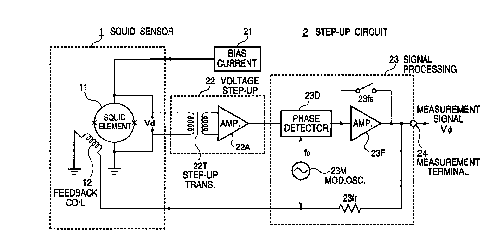
Referring to Figure 2A, there is shown a voltage step-up circuit 2
for a SQUID magnetometric sensor 1 according to a first embodiment of
the present invention. The magnetometric sensor 1 is provided with a
1 0 SQUiD element 11 and a feedback coil 12, and circuit 2 is provided with
a bias current source circuit 21, a voltage signal step-up means 22 and a
signal processing means ~3.
The SQUID element 11 is, for example, an oxide type of high-
temperature superconducting SQUID in which a thin film of HoBaCuO is
15 formed on a substrate of SrTiO3. The heart of the SQUID element is
superconducting junction which is formed by depositing the
superconducting thin film on the substrate having a step of 0.2 ~lm
(micrometers). This kind of SQUID element has advanced perforrnance of
high resolution, for example, one fifty-millionth (2x10⁻⁸) of the earth
2 0 magnetism.
When the SQUID element 11 is used as a magnetometric sensor,
it is placed in liquid nitrogen to operated in a temperature ambience of
-196~C together with the feedback coil 12. For example, the feedback coil
12 is formed on the substrate with a conductor thin film of only one turn
25 to contribute to the simplification of the SQU~D sensor construction.
Additionally, the feedback coil, in operation, receives an exciting signal
from the processing circuit 23, and applies a certain mod~ e(3 magnetic
- 10-
CA 02223767 1997-12-04
field and a feedb~k magnetic field to the SQUID element l I based on the
detection result of a voltage Vd detected by the SQUID element
The voltage step-up circuit 2 is an electronic circuit which drives
the SQUID sensor 1 and processes a voltage signal representing the
5 detected voltage Vd from the SQUID element 11, using the means 21 to
23 forrning a magnetic flux moduladon type of magnetic flux locked loop,
so-called "FLL." The bias current source circuit 21 produces an AC bias
current having a relatively low frequency fl, for example, 1 kHz, or a
certain DC bias current to supply the bias current. The voltage signal
10 step-up means 22 steps up and amplifies the detected voltage signal Vd.
Also, the signal processing means 23 includes an oscillator circuit 23M
for generating a modulation signal, a phase detector 23D, a feedback
integrating amplifier circuit 23F, and the like.
The oscillator circuit 23M generates the modulation signal of a
15 relatively high frequency fo, for example, 1 kHz, arld accordingly excites
the feedback coil 12 depending on this modulation signal to apply a
certain magnetic field to the SQUID element. The phase detector 23D
detects a stepped up voltage signal from the ste~up mear~s 22 on the basis
of the modulation signal. In addition, the feedback integrating amplifier
2 0 circuit 23F, having an integration function and reset by a reset switcl~
23fs, excites the feedback coil 12 through a feedback resistor 23fr
depending on the detection of the detected voltage Vd to apply the
feedback m~gT etic field to ~e SQUID element l 1.
This circuit of FLL type uses a null method technology, as well
2 5 known. Namely, the feedback integrating amplihler 23F feedbacks the
exciting current corresponding to the detected voltage signal Vd to the
feedback coil 12, thereby the feedback coil 12 applies the feedback
.CA 02223767 1997-12-04
magnetic field to the SQUID element 11 to cancel an external m~grlP~tic
field to be measured, and consequently the operating point of the SQIJID
element 11 is autom~tic~lly null-bqlAneed to be locked at a trough or crest
point of a SQUID voltage (V) vs. magnetic flux (~) characteristics curve.
5 Therefore, the e~citing signal produced by the feedback integrating
amplifier 23F represents the external magnetic field to make a desired
magnetic field measurement signal V~ appear on a measurement output
terminal 24, with the above FLL function.
10Now, according to the present invention, the voltage signal step-up
means 22 includes a ste~up transformer 22T and an electronic amplifier
22A, in which the transformer 22T isolates electrically its input stage
from the following stages and steps up the detected voltage Vd to a
required voltage of a certain multiples of the voltage Vd, and the
15 amplifier 22A amplifies the stepped up voltage to obtain a signal to be
processed.
The step-up transformer 22T has, for example, a ferrite core
wound with primary and secondary windings in a predetermined turn
ratio, for example, a selected value between several and hundreds,
2 0 depending on the specification of the SQUID element and the ampli~ler
22A. It is already cor~lrrned by the Inventors that the step-up transforrner
22T has the voltage fluctuation and noise ratio negligibly small and has no
problems in practice, though it is placed remotely from the SQUID
element 11 and at variable room temperature.
2 5Another consideration is that thermal noise owing to a resistance
component is generally proportional to the absolute temperature (K).
Here, as contrasted with a sensor structure containing a step-up
- 12-
CA 02223767 1997-12-04
transformer in the prior art in which it might be considered to have used
a usual SQUID operating at 4 K = -269~C or below, a SQU~D element of
an o~ide type of high-tc~ ture operates, for example, at 77 K = -
196~C, in the present invention. Accordingly, a detected voltage generated
S by this SQU~D element in the present invention has already included the
thermal noise component four times the thermal noise of the usual SQUID
[4 _ (77/4)1/2 ] in the prior art. Thus, it can be considered that a ste~up
transformer, though remote from the sensor and placed at room
temperature, does not exen such an effect on the detected voltage as a
10 noise source, and accordingly the step-up transformer can work
effectively ~ough placed on dle side of a SQUID driver circuit at room
ten~lature with no obstacles in practice.
High-pass Filter Function
The ste~up transformer performs not only the above voltage ste~
up but also a high-pass filter function for passing effectively high-
frequency components by selecting its circuit constants of suitable values.
The high-pass filter function is explained as follows.
In the voltage step-up circuit 2 processing signals with magnetic
2 0 flux modulation, the detected voltage signal Vd generated by the SQUID
element 11 includes a high-frequency component fo of the modulation
signal generated by the oscillator circuit 23M. The voltage signal Vd is
stepped up by the transformer 22T and amplified by the amplifier 22A in
the voltage signal step-up means 22, and furcher sent to the signal
25 processing means 23 to pick up only a desired compooent of the
frequency fo.
- 13-
~ CA 02223767 1997-12-04
Now, if the bias current source circuit 21 produces an AC bias
current having a component of a predetermined frequency, for example,
fl, to the SQUID element, the voltage signal Vd gelle,~led by the element
I l includes the component of the frequency fl. In particular, when the
AC bias current has the wave shape which is rectangular, the voltage
signal includes harmonic components of frequencies nfl. Therefore, it is
very useful to filter the component of the frequencies nfl as well as the
frequency f1. In the view of this point, the circuit according to the present
invention can be constructed to elimin~te the components of these
l O frequencies f1 and nfl by selecting suitable circuit constants of the ste~up transforrner 22T.
Here, assuming that the internal resistance of the SQUID element 11
is represented by Rs, the circuit resistance between the SQUID element 11
and the step-up transformer 22T is tepresented by Rc, the internal
resistance of the ste~up transformer 22T is represented by Rt, the coil
in~llct~nce of the transfolmer 22T is represented by Lt, and the resist~nce
Rt of the transformer 22T is sufficiently smaller than the resistances Rs
and Rc, the circuit comprising the SQUID element 11 and the step-up
transformer 22T is illustrated by an equivalent circuit of ~igure 3. As
2 0 shown in this equivalent circuit, it is understood that the transformer 22T
is allowed to act also as a high-pass filter, the cut-off frequency fc of ~his
filter is given by the following:
fc = (Rs + l~c) / (2~Lt). (1)
Therefore, the coil inductance Lt is given by the following:
2 5 Lt = (Rs + Rc) / (2J~fc). (2)
In the present invention, the cut-off frequency fc is selected in the
region as follows:
- 14-
, CA 02223767 1997-12-04
fo > fc ~ fl, (3)
to deterrnine a desired value of the coil inductance Lt of the set-up
transfonner 22T. In the example of fo = 40 kHz and fl = 1 kHz as shown
in Figure 2A, the value of the cut off frequency fc, for exarnpIe, fc = 10
5 kHz, is selected according to equation (3) and a desired coil in~ ct~nce Lt
is obtained by equation (2) based on this value of fc and given re.cist~nce
values Rs and Rc.
In addition, when the output voltage Vd of the SQUID element 11
has noises of sufficiently lower frequencies than the modulation signal
10 frequency fo, these noises are efficiently elimin~ted by the above high-
pass filter function of the step-up tra~sformer 22T. Therefore, the high-
pass filter acts effectively on low frequency noise included in the SQUID
output voltage Vd, both in the case of DC current bias as well as the above
AC bias current of frequency fl.
1 5
Applied Example
The ste~up circuit according to the first embodiment of the present
invention allows relieving the designing and fabricating of magnetometric
sensors from various restrictions owing to using a first step-up
20 transformer within a narrow SQUID sensor at a very low t~ ure,
and accordingly provides a magnetometric sensor that is inexpensive and
easy to handle. Therefore, the present invention is applicable to various
technical fields.
In Figure 4, there is shown a schematic circuit block diagram of a
2 5 SQUID driver, as an example of applying a step-up circuit according to
the present invention, in which the step-up circuit is applied to a
magnetometer in "a circuit device for driving a magnetometric sensor" of
~ CA 02223767 1997-12-04
the above mentioned J~ nese Patent Application. In this e~cample, the
above mentioned advantages are provided.
Additionally, the SQUID driver circuit of Figure 4 has mai~ly the
m~n~tometer for driving a SQUID element 11 as a rn~netQmetric sensor
5 and obtaining a magnetic field measurement signal V~ to determine an
external magnetic field, and an evaluator for obt~ining a current or
magnetic flux signal I or ~ depending on the ch~n~ing operation "i/~" to
estimate SQUID characteristics, such as V-~ and V-I characteristics. In
this circuit, a feedback coil 12 within a SQUID sensor 1 is also used as a
10 magnetic field applied when the evaluator is selected. The SQUID driver
circuit allows mainly to perform either a magnetometer function or an
evaluator function by changing their power supply depending on a
selector. For its details, please see the above description.
1 5 Sccond Emb~lim~-.nt
Even the above voltage step-up circuit according to the first
embo-liment of the present invention requires many terminals as shown in
Figure 2B. Figure 2B shows in partial detail a schematic block diagrarn of
the same voltage ste~up circuit as Figure 2A, consequently the identical
2 0 numerals indicating the same elements ben~een Figures 2A and 2B are
used, but Figure 2B also illustrates the tern~inals and wirings of a voltage
step-up circuit 2 to a SQUID magnetometric sensor 1 in detail.
As shown in Figure 2B, it is easily understood that the voltage step-
up circuit requires at least four signal terminals tbl, tb2, tdl and td2 for
25 one SQUID element, further two signal terminals tfl and tf2 if
considering magnetic feedback, similarly to the system shown in Figure
lB. To alleviate this problem, according to a second embodiment of the
- 16-
CA 02223767 1997-12-04
present invention, these four or six signal terminals and wirings for one
SQUID sensor are effectively reduced in half, the quantity of a cooling
medium is also reduced correspondingly, and consequently the cooling
effect of the SQUID is increased.
~ow, Figure 5 shows a schematic circuit block diagram of a voltage
step-up circuit according to the second embodiment of the present
invention. A SQUID magnetometric sensor 1 is provided with a SQUID
element 11 and a feedback coil 12. On the other hand, a voltage step~up
circuit for driving the SQUID sensor 1 and processing signals is provided
with a bias current source circuit 21, a voltage signal step-up means 22
including a step-up transformer 22T, and a signal processing means 23
This voltage step-up circuit 2 is also provided with a signal input/output
terminal tl, a cornrnon potential terminal to and a feedback exciting
tennin~l t2 in order to transrnit / receive signals to and from the SQUID
sensor 1. The cornmon terminal to is electrically connected commonly at
least to each one of the current outputs of the bias current source 21, the
primary inputs of the step-up transformer 22T and outputs of the
feedback stage in the signal processing means 23. A common reference
potential, for example, the ground potential or a base board potential is
2 0 applied to ~e tt~ n~l to and these inputs and outputs.
In the SQUID sensor, the SQUID element 11 and the feedback coil
12 are formed by the technique similar to that mentioned above, and
placed in conditions similar to those mentioned above. However, they are
electrically connected to the terminals to, tl and t2 with only three wiring
2 5 conductors of, for example, signal cable. Namely, each one end of the
SQUID element l l and the feedback coil 12 is commonly conne~ted to the
common potential tenninAl~ to with the first conductor, _nd the other end
CA 02223767 1997-12-04
of the element 11 is connected to the signal input/output terminals tl with
the second conductor. The other end of the coil 12 is connected to the
feedback e~cciting terminals t2 with the third conductor for receiving a
feedback e~citing signal from the fee-lbac~ stage of the signal procescin~
5 means 22 to apply a corresponding magnetic field to the element 11.
The vo1tagc step-up circuit 2 is formed as a magnetometer circuit
with FLL to drive the SQUID sensor and to step up and process a detec~e~
voltage signal Vd representing a voltage generated by the SQUID element
11, as already explained.
10The bias current source circuit 21 produces an AC bias current
having a relatively low frequency, for example, 1 kHz, or a certain DC
current between its outputs connected electrically to the terrninals to and
tl, in order to supply the bias current to the SQUID element 11.
The voltage signal step-up means 22 includes the step-up
15transformer 22T and an electrotuc amplif1er 22A. The transformer 22T is
connected between the termin~l.s tl and to tllrough a resistor 22R having a
predetermined value as explained in details hereinafter, in order to step
up effectively the detected voltage signal Vd from the SQUID element 11
to a predetçnnined multiples of the signal Vd. The amplifier 22A further
2 0 amplifies the stepped up signal to a suitable value to be processed by the
following stages.
The signal proces.cing means 23 includes an oscillator 23M, a phase
detector 23D, a feedback integrating amplifier 23F, and the like, in order
to process the stepped up and amplified signal to obtain a magnetic flux
2 5 measurement signal V~ on a measurement terminal 24, with the FLL
function, as explained in detail hereinbefore in connection with Figure
2A. Consequently, the identical numerals indicate the same elements
- 18 -
CA 02223767 1997-12-04
between Pigures 2A and 5. But, in Figure 5, outputs of a feedb~c~ stage
of the processing means 23 are electr~cally connecte~ to the terrnin~l~ t2
and to in order to apply a modulated feedback exciting signal between
terminals t2 and to depending on the feedback quantity based on the
s voltage detection signal Vd and the modulation by a modulation signal
having a relatively high frequency fo .
Additionally, the step-up transformer 22T is also the same as the
rst embodiment, and accordingly many advantages of the first
embo.lim~.n~ can be obtained as explained hereinbefore.
1 0
Here, in the voltage step-up circuit according to the second
embodiment of the present invention, the outputs of the bias current
source circuit 21 are electrically connected to the signal input/output
terrninal tl and the common terminal to to supply the bias current to the
1 5 SQUID element 11, and the primary inputs of the step-up transformer
22T are also conn~ctetl to these termin~ls tl and t~ to receive the detecte~l
voltage signal Vd from the SQUID element 11 through the series resistor
22R, as above mentioned. The resistance value of the series resistor 22R is
selected so as not to saturate the core of the step-up transformer 22T,
20 depending on the inner resistance of the transformer 22T and wiring
resistance of the signal cable. Accordingly, the value is relatively small,
for example, about lQ. This allows use of a circuit structure of a type
called "two terminal manner," that is, one set of two tçrmin~l.c tl and to
providing both functions of bias current supplying and SQUID voltage
2 5 receiving .
Figures 6A and 6B are illustrations for explaining that the voltage
step-up circuit constructed in "two terminals manner" according to the
- 19-
CA 02223767 1997-12-04
present invention is capable of supplying effectively a desired bias current
to the SQUID element 11 as well as stepping up effectively the voltage
signal detected by the SQUID elernent l I to be effeclively picked up by
the trans~ormer 22T.
In Figure 6A, there is illustrated an equivalent circuit to the circuit
between a SQUID element 11 and a step-up transformer 22T in a circuit,
where the type of the circuit is simply changed into "two terminals
m~nn.o.r" from "four terminals m~nn~.r" shown in Figure 2B, and thereby
first terr nals tbl and tdl and second termin~lc tb2 and td2 are unified to
terminals t'1 and t'o, respectively. Additionally, in Figure 6A and 6B, Rb
represents equivalent bias path resistance through a bias current supplying
path between the terminals t'l and t'o, including the sum of internal
resistances of the bias current source circuit 21 and the wiling conductor
of the path, for example, about 1 kQ. Rs represents equivalent sensor
resistance through the SQUID path between the terminals t'l and t'o,
including internal resistance of the wi~ing conductor, such as a signal
cable between the SQU~D sensor 1 and the circuit 2, for example, about 1
to S Q. And, Rt represents equivalent transformer resistance through a
transformer path between the terminals t'l and t'o, including the sum of
2 0 internal resistances of the set-up transformer 22T and the wiring
conductor of the path. This value is almost zero. Consequently, the
equivalent transformer resistance Rt is sufficiently smaller than the
equivalent sensor resistance Rs.
In the equivalent circuit of Figure 6A, almost all the current from
the current source 21 flows through the transformer path because ~e
transformer resistance Rt is sufficiently smaller than the sensor resistances
Rs. As a result, the step-up transformer 22T w~rks in a saturation region
- 20 -
, CA 02223767 1997-12-04
of magnetization characteristics curve of the transformer core, and
accordingly cannot perform effectively the step up transforming.
Now, referring to Figure 6B, there is illustrated an equivalent
circuit to the circuit between a SQUID element ll and a step-up
transformer 22T in the voltage step-up circuit of the present invention
shown in Figure 5, where Rb, Rs and Rt represcnt respcctively equivalcnt
resistances through the bias current supplying path, the SQUID path and
the transformer path except the series resistor 22R between the termin~l~
t'l and t'o, ~imil~rly as Figure 6A. And, a limitation resistance Rr
l O represents the resistance value of the series resistor inserted in the
transformer primary path.
In the equivalent circuit of Figure 6B, because the limitation
resistance Rt is selected so as not to saturate the transformer.core as
already mentioned, the current flow from the current source 21 is
separated suitably to the SQUID element 11 and the ste~up transf~nner
22T, and accordingly the current through the transformer 22T is not so
much as to saturate the transformer 22T. Therefore, the core of dle
transformer is not saturated by the current that steps up effectively the
voltage signal detected by the SQUID element 1 l.
In addition, for the feedback exciting signal, it may be also adopted
that two feedback terminals, such as tfl and tfl of Figure 2B, are
separated off from the common potential terminal to in Pigure 5 for
technical consideration.
2 5 In the case that the common t~rmin~l to is used together with the
feedback terminal t2 for applying feedback excitation as shown in Figure
5, the fee~b~k excitation func~ion can be added by providing only three
- 21 -
~ CA 02223767 1997-12-04
terminal for the whole SQUID sensor 1. Therefore, in this case, the step-
up circuit 2 for driving tne magnetometric sensor I with FLL allows to
further increase the effects of reducing the number of wirings and the
quantity of a cooling medium.
- 22 -