Note: Descriptions are shown in the official language in which they were submitted.
CA 02224300 2006-06-23
- 1 -
DISCHARGE LAMP DRIVING BRIDGE CIRCUIT
Background
This invention relates to driving discharge lamps.
s High-intensity discharge (HID) lamps, specifically
pulse start metal halide discharge (MHD) lamps, place
demanding requirements on the ignition pulse. The
ignition pulse amplitude specified by the lamp
manufacturer is typically high, though it varies between
1o manufacturers. For example, for reliable starting,
Philips Lighting specifies a pulse peak 10 greater than
3.3kV (see Fig. 1). Apart from the peak pulse amplitude,
the pulse must be sufficiently wide 12, typically 1.5-
2.5~.
i5 In electronic ballast, the required ignition pulse
is most commonly generated by charging a capacitor and
then discharging it into the primary of a pulse
transformer. The secondary to primary turns ratio of
this transformer is typically greater than 100. A very
2o high voltage is thus generated across the secondary.
This voltage is coupled across the lamp to strike the
arc. Various other components such as inductors,
resistors and capacitors are used to shape the ignition
pulse to meet the requirements set forth by the lamp
2s manufacturers. Design of the ignitor circuit is one of
the most critical parts in the ballast because it can
affect the lamp life. The peak pulse requirements are
relatively easy to meet; but the pulse-width requirements
cannot be met easily. The high peak value adds, stress on
so the ignitor transformer and requires special insulation
and construction. Also, the peak current in the primary
circuit can be as high as 15-20A. U.S. patent 5,517,088
describes one implementation. The pulse peak and the
pulse-width requirements add significant cast to the
ss ignitor circuit.
CA 02224300 1997-12-10
- 2 -
As seen in Fig. 2, pulse ignition also adds
minimum open-circuit voltage (Voc) requirements since the
open circuit voltage determines the glow to arc
transition. Most lamps are designed to operate on AC
s voltage/current and this makes the time 14 from
application of the ignition pulse to voltage polarity
reversal critical. If the polarity reversal occurs too
soon after the ignition pulse, the arc may not go
completely from glow to arc transition and it may
io extinguish. The requirement for this minimum time
normally implies that the frequency of voltage applied
across the lamp during starting must be sufficiently low
(20-30 Hz) and must be increased (150-200 Hz) once lamp
starts. This requires extra control circuitry.
1s In a typical pulse ignitor, the lead capacitance
degrades the ignitor performance. For this reason the
lead lengths are typically kept to a minimum. U.S.
patent 5,517,088 describes an implementation that reduces
this effect.
2o Starting the lamp at high-frequency (>30kHz)
lowers the required peak of the ignition voltage. It is
believed that applying a burst of high-frequency pulses
for a period of time is equivalent to applying a wide
pulse for that time. The fast transition from a peak of
2s one polarity to the peak of opposite polarity makes the
peak-to-peak voltage and not the peak voltage the
effective ignition voltage. Capacitive discharge
currents at high-frequencies within the arc-tube and to
nearby ground planes may also play some role in the
3o reduction of the required pulse amplitude. It has been
found that the peak pulse requirements are reduced almost
by a factor of two at high frequency. Experience has
shown that if the peak is kept below 2.5kV the stress on
the ignitor transformer is considerably reduced. Also,
3s the risk of corona breakdown between ballast terminals
CA 02224300 1997-12-10
- 3 -
and within the ignitor transformer is significantly
reduced. Corona breakdown becomes an issue when the lamp
fails and the ballast continues to apply high voltage
pulses to try to start it. To minimize potential
problems under such a situation a shutdown circuit is
required that shuts down ballast operation after a
predetermined time, typically 20 minutes. Since high-
frequency starting significantly reduces the peak voltage
requirements it makes the system more reliable, and
1o perhaps smaller and cheaper.
In the realm of fluorescent lamps, resonant
circuits are popular for operating fluorescent lamps at
high frequency. These circuits have significantly
reduced the cost and size of electronic fluorescent
ballasts. A resonant circuit also allows ease of
starting of the lamp since high voltages can be easily
generated in an unloaded series-resonant circuit.
HID lamps typically cannot be operated at high-
frequency due to acoustic resonance problems. One major
lamp manufacturer has a specially tuned high-frequency
ballast for their HID lamps. This ballast utilizes a
series-resonant circuit that starts the lamp at high-
frequency. A new high-frequency technique utilizing
white noise modulation is discussed in the latest work
done by Laszlo Laski at Texas A&M University, "High-
Frequency ballasting Techniques For High-Intensity
Discharge Lamps," Ph.D. Dissertation, 1994. This
approach also utilizes a series-resonant circuit in the
output. This high-frequency technique is very new and
3o there is not enough test data to assure its universal
application. Thus, low frequency square wave operation
remains a most popular technique for electronic HID
ballasts.
As seen in Fig. 3A, a typical electronic HID
ballast 30 is a three-stage power processing device. The
CA 02224300 1997-12-10
- 4 -
first stage is a boost power-factor correction (PFC)
stage 32. This stage insures that the current drawn by
the ballast is in phase with the line voltage 33 and has
low distortion. The second stage is a buck power control
s stage 34. This stage regulates the lamp power and limits
the current in the lamp during the warm-up phase. The
final stage is a full-bridge inverter 36 that takes the
buck regulator's output; which is DC, and converts it to
a low-frequency square wave (AC) for the lamp. In
1o addition to these stages there is also a pulse ignitor
circuit 38. Some ballasts (see Fig. 3b) combine 39 the
buck stage and the output full-bridge inverter. A pulse
ignitor 38 is invariably required to ignite the lamp.
U.S. Patent 4,912,374 describes a high-frequency
15 resonant ignition topology in which the power control
stage and the inverter stage are combined in a half-
bridge/full-bridge topology (Figs. 5a and 5b). A
disadvantage of this scheme is that since the power
control (buck) stage is combined with the output
2o inverter, in order to prevent acoustic resonance, the
output inductor 20 and the capacitor 22 across the lamp
must provide sufficient filtering to keep the high-
frequency component of the lamp current to a minimum.
Consequently, the value of the capacitor is large, in the
25 order of 1/10 micro farad. This scheme operates the lamp
at high-frequency and low frequency alternatively. When
this circuit is operated at high-frequency and the lamp
is off, the resonant circuit formed by the inductor and
capacitor produces high voltage to ignite the lamp.
so Because of the large capacitance value and relatively
smaller inductor value very large circulating current
flows in the circuit. This large circulating current
must be supported by all components of the circuit
causing high stress on all parts. When the lamp is and
3s operating in the high-frequency mode, the circuit
CA 02224300 1997-12-10
- 5 -
produces high-frequency current in the lamp. During the
low-frequency mode, the switching pattern is changed to
one that would control the lamp power and limit the lamp
current. This scheme calls for increased complexity of
the control circuit and the circuit components must be
selected carefully.
Another scheme, similar to the one above, is
described in Japanese patent 94P01476. Here (Fig. 6) the
power control and current limiting function is provided
1o by a preceding buck converter stage. The advantage of
this circuit over the ones described in U.S. Patent
4,912,374 is that the value of the capacitor will be much
lower and, thus, the circulating currents are not as
high. A disadvantage of this scheme is that it needs
i5 four high-frequency switches 24, 26, 28, 30 and the high
side switches need to be driven by more expensive drivers
21, 23 to achieve efficient drive. The lamp is again
operated at high-frequency 25 and low-frequency 27
alternately.
20 In the above schemes during the time the lamp
operates at high-frequency, the current is largely
determined by the value of DC bus voltage 31, frequency
of operation, and the value of the inductor. The DC bus
voltage is normally fixed by other considerations.
25 Frequency can be used to control the current to a certain
extent, but since the circuit must operate close to
resonance to produce high-voltage, it cannot be used as
an effective control. For proper operation, sufficient
current must flow through the lamp during high-frequency
30 operation. This implies that the value of inductance
must be low. To keep switching losses low, the resonant
frequency must be kept low. To keep the resonant
frequency from increasing because of lower inductance
value, the value of the capacitor must be increased. The
35 overall effect is that the circulating currents increase.
CA 02224300 1997-12-10
- 6 -
To reach a compromise the lamp current during high-
frequency operation may be lower than the desired value.
Summary
In general, in one aspect, the invention features
a discharge lamp driving circuit which includes DC
voltage input connections, lamp driving connections,
bridge circuitry, and control circuitry. The bridge
circuitry is connected to the DC voltage input
connections and to the lamp driving connections and
1o includes circuit elements which in one mode of operation
deliver a higher frequency AC voltage to the lamp driving
connections and in another mode of operation deliver a
lower frequency AC voltage to the lamp driving
connections. The control circuitry is connected to
control the bridge circuitry selectively as either a
half-bridge to deliver the higher frequency AC voltage to
the lamp driving connections during starting or a full-
bridge to deliver only the lower frequency AC operating
voltage to the lamp while the lamp is operating normally
2o after starting.
In general, in another aspect, a low frequency
driver and a high frequency driver are connected to drive
the bridge circuitry so that in one mode of operation a
higher frequency AC voltage is delivered to the lamp
driving connections and in another mode of operation a
lower frequency AC voltage is delivered to the lamp
driving connections.
Implementations of the invention may include one
or more of the following features. The bridge circuitry
3o may include four unidirectional conducting portions
connected in a bridge configuration. The bridge
circuitry may include a resonant circuit having an
inductor and a capacitor, the inductor being connected to
one of the lamp driving connections. The control
circuitry may be connected to sweep the frequency of the
CA 02224300 1997-12-10
AC voltage during starting through a range that includes
a resonant frequency of the resonant circuit. The
capacitor may also be connected to the one of the lamp
driving connections. The capacitor may be connected to a
s tap of a winding of the inductor. The control circuitry
may be connected to drive the bridge circuitry at
essentially a resonant frequency of the resonant circuit.
The low frequency driver may be connected to drive two of
the switches at DC on or DC off during starting, and a
1o high frequency driver may be connected to drive the other
two of the switches. The control circuitry may be
connected to the low frequency driver to drive one of the
two switches (e.g., the lower switch in Figs. 7A, 7B) at
DC during starting.
1s The one pair of switches may be connected in
series across the DC voltage input connections, and the
other pair of switches may be connected in series across
the DC voltage input connections. The resonant circuit
may be connected between the commonly connected ends of
2o the two switches of the one pair and one of the lamp
driving connection, and the commonly connected ends of
the two switches of the other pair may be connected to
the other one of the lamp driving connections. The
control circuitry may be connected to control the bridge
2s circuitry to operate in the starting mode only until the
lamp is ignited.
The control circuitry may be connected to control
the bridge circuitry during starting to repeatedly and
alternately stop operation of the bridge circuit and to
3o continue operation in the starting mode. The control
circuit may be connected to control the bridge circuit to
deliver essentially DC to the lamp immediately after
starting.
In general, in another aspect, the invention
3s features driving a discharge lamp by operating a bridge
CA 02224300 1997-12-10
_ g _
circuit as a half bridge to deliver a higher frequency AC
voltage from bridge circuitry to the lamp during
starting, and operating the bridge circuit as a full-
bridge to deliver only lower frequency AC operating
s voltage from the bridge circuitry to the lamp during
normal operation after starting.
Among the advantages of the invention are one or
more of the following. The circuit for igniting HID
lamps is simpler. The peak of ignition voltage is
1o reduced by utilizing a high-frequency starting technique.
Stress on circuit components due to high circulating
current is reduced. Eliminating high-frequency operation
of the lamp eliminates the possibility of acoustic
resonance even though the circuit operates at high-
~s frequency during starting.
Other advantages and features will become apparent
from the following description and from the claims.
Description
Fig. 1 shows typical requirements of the ignition
2o pulse from a pulse ignitor.
Fig. 2 illustrates the open circuit voltage
requirements. In Fig. 2, Vo~ represents the open circuit
voltage, Vpk the peak of ignition pulse, and t the time
from ignition pulse to voltage polarity reversal.
25 Fig. 3 shows a block schematic of electronic
ballast for an HID lamp. Fig. 3(a) shows the block
schematic of a traditional three stage electronic ballast
for HID lamp which has a separate pulse ignitor circuit
while Fig. 3(b) shows the block schematic for a two stage
3o ballast in which the power control and inversion stages
are combined into one.
Fig. 4(a) shows the block schematic for the
proposed electronic ballast for the HID lamp and Fig.
4(b) shows a more general embodiment of the proposed
35 circuit.
CA 02224300 1997-12-10
_ g _
Fig. 5(a) and 5(b) show two of the embodiments of
U.S. Patent 4,912,374.
Fig. 6 shows the scheme described in Japanese
patent 94P01476.
s Fig. 7(a) shows a circuit schematic of an
embodiment of the invention while Fig. 7(b) shows an
alternate arrangement.
Fig. 8 shows gate drive waveforms during starting
and during normal operation (waveforms are exaggerated
1o for clarity) .
Fig. 9 shows typical operating frequency versus
time and the corresponding output voltage versus time.
Fig. 10 shows output voltage of the circuit under
no-load condition. Fig. 10(a) shows a timing sequence
15 that may be utilized to minimize the stress on parts
while Fig. 10(b) shows the actual output voltage at
power-up under no-load condition.
Fig. 11 shows lamp starting characteristic. Fig.
11 (a) shows lamp voltage and current relationship at
2o start-up while Fig. 11(b) shows the actual lamp current
and its transition form starting mode to normal running
mode.
In the invention, a full-bridge inverter circuit
and high frequency ignitor 42 (in Figs. 4A and 4B)
2s provide the HID lamp 44 with low-frequency current to
avoid acoustic resonance and a preceding power control
stage 32, 34 or 44 to limit lamp power and current. The
lamp is never operated at high frequency and hence there
is no chance of acoustic resonance. The circuit utilizes
3o a resonant tank formed by a series connection of an
inductor and a capacitor. The circuit is operated at
high-frequency close to the resonant frequency of the
tank. During the high-frequency mode the operation of
the switching devices is controlled in a manner such that
CA 02224300 1997-12-10
- 10 -
the full-bridge configuration is essentially converted to
a half-bridge configuration and the lamp gets connected
across the capacitor of the resonant tank. This
switching control scheme requires only two switches to
operate at high-frequency, thus reducing the number of
high-frequency switches required. It must be noted that
even though the circuit operates at high-frequency during
starting, the lamp current, once the lamp arcs, is DC
because of the circuit configuration and not high-
to frequency AC. Once the arc is established the lamp is
operated by low-frequency AC. In this circuit
configuration, the inductor and the capacitor values can
be selected so that the circulating currents during the
high-frequency operation are minimized and at the same
time the lamp current, as soon as the lamp arcs, can be
controlled at any desired value by the preceding power
control stage. In this configuration the stress on the
parts is significantly reduced.
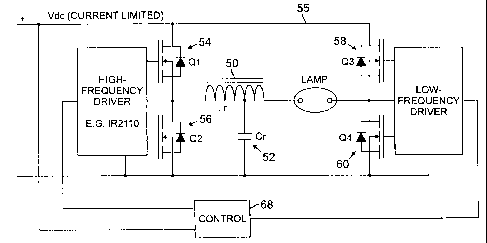
Fig. 7(a) shows an example of a circuit schematic
of the present invention. In Fig. 7(a) Lr is the
resonant inductor 50, Cr the resonant capacitors 52, and
Q1, Q2, Q3, and Q4 are switching devices with internal or
external anti-parallel diodes 54, 56, 58, 60. The four
switches are connected to form a full-bridge circuit. Lr
and Cr form a series-resonant tank.
The DC bus 55 (Voc) must be current limited since
the lamp current must be limited and the inverter stage
provides no control over the current. The bridge itself
can be protected from over-current and over-voltage
3o during the high-frequency operation by proper design of
Lr (Q of the circuit) and by proper frequency control.
Nevertheless, having a current limited DC bus provides
additional protection for the bridge components during
high-frequency modes and during output short circuit
conditions. In most HID ballasts a preceding buck
CA 02224300 1997-12-10
- 11 -
regulator stage or a combined power factor control (PFC)
and power control stage provides this function.
During normal lamp operation, the bridge operates
as a full-bridge, i.e., Q1 and Q4 conduct simultaneously
during one-half cycle while Q2 and Q3 conduct
simultaneously during the other half cycle, thus applying
a low-frequency bipolar rectangular voltage across the
lamp. The amplitude of Vd~ at any instant is function of
the lamp voltage and is controlled by the power control
to stage (not shown). Lr serves as a filter for the high-
frequency component of lamp current which arises due to
high-frequency ripple on the DC bus voltage (i.e., the
output of buck converter/power control stage) . The
resonant frequency of the tank is several orders of
magnitude higher than the normal operating frequency,
i.e., the value of Cr is very small and, thus, it does
not affect the normal operation of the circuit in any
significant way.
What happens during starting is different from the
2o normal operating mode and from operation of known
circuits. Fig. 8 shows exaggerated gate drive waveforms
during starting and during normal operation. Q1 and Q2
(or Q3 and Q4) never conduct simultaneously because, if
they do, they will short Vd~. It will also be noticed
that Q4 is ON continuously and Q3 is OFF continuously
during the start-up high-frequency mode, while Q1 and Q2
switch at high-frequency. This mode of operation
essentially converts the full-bridge to a half-bridge.
There are several important features of this half-bridge
operation as compared to operating the resonant circuit
as a full-bridge. First, only two transistors, Q1 and
Q2, operate at high-frequency and, thus, only one high-
frequency driver is required (high-frequency high-side
drivers cost significantly more than low-frequency
drivers). A high-frequency driver is not required for Q3
CA 02224300 1997-12-10
- 12 -
and Q4. Also, slower transistors can be used for Q3 and
Q4 if so desired (slower transistors are normally
cheaper). Second, the driver for Q3 and Q4, which
operates at low frequency, is simplified and the cost can
s be reduced considerably. Third, Cr can be placed as
shown in Fig. 7 instead of across the lamp. This
eliminates the need for Q4 to carry the high circulating
currents during the high-frequency operation. This is
not possible in a full-bridge operation shown in Fig. 6.
1o As shown in Fig. 7(a), Cr can be placed on a tap of Lr
winding. This provides a voltage boost across the lamp
while keeping the voltage across Cr the same. Up to 400V
can be easily added to the peak of the output voltage by
few extra turns on Lr. It must be noted that this
1s construction of Lr is not a requirement for proper
circuit operation and Fig. 7(b) shows a circuit
implementation where Cr is connected directly to one end
of Lr. One of the main differences between the full-
bridge and half-bridge starting is the current through
2o the lamp after ignition while the circuit is still in
high-frequency mode. In the full-bridge operation this
current is AC with no DC off-set and, as mentioned
earlier, its value is largely determined and limited by
the value of Lr and the DC bus. In the half-bridge
2s operation of the circuit shown in Fig. 7, the lamp
current is DC with a high-frequency ripple component
superimposed on it. The DC value of current is
determined by the current limit of the preceding power
control stage, while the ac ripple is determined by the
3o value of Lr, the operating frequency and the DC bus
voltage, and is small compared to the DC value. The
current limit set by the preceding power stage is crucial
both for the normal warm-up of lamp and for generating
sufficient voltage to strike the arc. If this value is
35 set too low, the circuit may not produce a high-enough
CA 02224300 1997-12-10
- 13 -
voltage to strike the arc or the current may be too low
to warm-up the lamp once it arcs. If this limit is set
too high, it will degrade lamp life and it will cause
additional stress on the circuit components under short-
s circuit conditions of output.
The AC nature of the current in full-bridge
operation may be a disadvantage since its value is
significantly lower (limited by Lr) when compared to the
value of DC (limited by current limit of preceding buck
1o stage) for half-bridge operation on the same circuit.
The lower value of current will not heat the electrodes
fast enough and will adversely affect the lamp life (this
is like dimmed operation).
The advantage of high-frequency resonant ignition
1s over the pulse ignitor is that the open-circuit voltage
is no longer a critical factor. This is because the
voltage across the lamp self adjusts forcing a quick and
smooth transition from glow to arc. During the glow mode
the lamp impedance is high and this causes the resonant
2o tank to get unloaded increasing its Q which increases the
voltage across the lamp. On the other hand, during the
normal arc the lamp impedance is low and this causes the
resonant tank's Q to lower reducing the voltage across
the lamp.
2s Yet another advantage of the circuits shown in
Fig. 7 over the pulse ignitor is that the stray cable
capacitances are effectively placed across the resonant
capacitor. This would affect the resonance frequency
somewhat, but would not degrade the performance to an
3o extent the performance of the pulse ignitor would be
degraded.
As mentioned earlier, during starting, one leg of
the bridge is operated at high-frequency while the other
leg is operated so that it converts the full-bridge into
3s a half-bridge (see Figs. 7 and 8). To get maximum
CA 02224300 1997-12-10
- 14 -
voltage gain, the frequency of operation is ideally the
resonant frequency of the tank,
f = 1
2 Ti LrCr
This however is not possible in production, unless some
sort of feedback is used, because of component
tolerances.
For this reason, the frequency during the high-
frequency operation is not kept constant, but is swept
over a predetermined range 60 (Fig. 9) so that it will
1o cross the resonance point 62 at some instant so a high
peak voltage is applied across the lamp. Thereafter for
the remainder of the high-frequency period the frequency
is kept at a certain minimum value 64 to generate a
certain minimum voltage. For example the nominal
resonance frequency can be selected to be 50kHz. The
tolerances of Lr (~ 5%) and Cr (~ 5%) can easily cause
~5% variation in the resonant frequency. This would
cause the resonance frequency of the tank to vary from
52.5kHz to 47.5kHz. To allow for tolerance of the
2o frequency generator (~ 5%) the frequency sweep is started
at 60kHz. The sweep time 66 is in the order of 100mSec.
The idea is to catch the resonance peak as close as
possible or sweep through it. The frequency at the end
of the sweep is about 46kHz (determined experimentally)
2s and is maintained at that value for the remainder of the
high-frequency period. Fig. 9 shows an exaggerated plot
of switching frequency Fs versus time and the open-
circuit output voltage versus time.
The exact values of the open-circuit voltage
3o during high-frequency operation depends on the resonant
frequency of the tank, the Q of the tank, and the final
frequency value. The circuit must be designed to insure
CA 02224300 1997-12-10
- 15 -
at least 1.2-l.5kV for the final value of open-circuit
voltage. The peak voltage value is a function of the
saturation characteristic of the core, core and copper
loss in Lr (Q of the tank), and to a degree the amount of
current available from the preceding buck stage, its
regulation. A 2-2.25kV of peak value is desirable.
The characteristic shown in Fig. 9 is determined
through experimentation. It is found that having a
higher value of voltage "V" at the end of the sweep, V,
to and having a longer period for time "T" is helpful in
starting stubborn lamps. A high value of peak voltage is
no good if the final value of voltage is too low. The
optimum value of time T is found to be between 400-600mS.
Sufficient time must be allowed for the lamp to stabilize
(go completely from glow to arc) before switching to low
frequency operation. On the other hand, if too long a
time is provided, the DC current flowing through the lamp
may adversely affect lamp life. To minimize the circuit
complexity the high-frequency operation is done in open
loop, i.e., even if the lamp arcs the circuit continues
to operate at high-frequency for a predetermined time and
no effort is made to control the frequency to match the
resonant frequency of the tank. The high-frequency mode
of operation adds stress to the circuit components (Q1,
Q2, Lr and Cr) if it continues for too long and it is
thus another factor affecting the maximum value for T.
Near resonance, the circulating currents are fairly high
and Cr and Lr are subjected to high voltages at the same
time. Also, for below resonance frequency operation, Q1
3o and Q2 experience hard switching (the circuit operates in
this mode for most of the high-frequency period). Also,
since the lamp may not turn on in the first attempt
(because it is still warm from previous operation or is
difficult to start due to age), the circuit must keep
trying to start it for at least 20 minutes. Thus, the
CA 02224300 1997-12-10
- 16 -
circuit must be operated in the high-frequency mode
repetitively. The control circuit 68 (Fig. 7a) is
designed so the ballast tries to start the lamp
approximately every 1.5 seconds for the first 10-15
seconds from power-up, to quickly start the lamp.
However, if the lamp fails to start in this time an
attempt is made every 4-4.5 seconds thereafter for
approximately the next 20 minutes. If the lamp does not
turn on in 20 minutes the ballast shuts off and the power
to must be recycled before it will re-start.
Fig. 10(a) illustrates this sequence, while Fig.
10(b) shows the actual circuit voltage immediately after
power-up. Implementation of control is very simple. The
lamp ON/OFF condition is easily sensed by the DC bus
is voltage at the inverter input. When the lamp is OFF this
voltage is high, typically 200-300V, while when the lamp
is ON it is fairly low, 20V at lamp start-up and 80-115V
under normal running condition. To allow for increase in
lamp voltage due to aging, a lamp OFF condition may be
2o established when the DC bus is greater than 150V. If the
lamp is detected to be OFF, the control starts the high-
frequency ignition cycle described above and, once lamp
turns ON, the high-frequency cycling is stopped.
In all likelihood the lamp will start in the first
25 100-300ms of the applied high-frequency starting voltage.
Some lamps require lower voltage to start and may take
even shorter time to start. Fig. 11(a) illustrates the
lamp voltage and lamp current in this situation. Fig.
11(b) shows the actual lamp current and an expanded time
3o scale plot of transition from high-frequency starting to
low-frequency normal operation region.