Note: Descriptions are shown in the official language in which they were submitted.
CA 02224575 1997-12-12
WO 96/42097 PCT/DK96/00257
1
A METHOD OF PRODUCING AN ELECTRICAL SWITCH
The present invention relates to a method of producing an
electrical switch comprising a housing at least partially
enclosing switching means for cooperating with a set of at
least two metallic terminals, each terminal having an
exterior portion outside the housing and an interior portion
inside the housing.
In relation to switches of this type it is extremely impor-
tant to reduce the manufacturing costs. Any factor that in-
creases the number of switches produced in a given period of
time with the same personnel, factory space and discrete
units of production equipment is essential for the competi-
tiveness of the finished switch in the marketplace.
It is therefore an object of the present invention to provide
a method of producing such switches in which such an in-
creased production capacity is obtained as compared with
prior art methods.
A method for producing keyboard switches is known from Euro-
pean Patent No. 0 329 968 in which a single row of sets of
metallic terminals is punched out of a strip of the base
metal of the terminals, a housing is moulded around each set
of terminals, switching means are installed in each housing
and each set of terminals is thereafter separated from the
strip. In this method the necessary moulding and installing
operations are confined to a single production track defined
by the single row of sets in the strip.
A method for producing push button switches is known from
US Patent No. 4,803,316 in which two parallel rows of sets of
' terminals are punched out of a strip, and a housing frame is
moulded on each set whereafter the sets are separated from
the strip and processed individually for installing the
switching means. In this method the individual processing of
each discrete set of terminals with attached housing frame
CA 02224575 1997-12-12
WO 96/42097
PCT/DK96/00257
2
requires a number of additional handling steps for insertion
in, guidance through, removal from and transportation between
the various work stations corresponding to the subsequent
steps of installing the switching means in each individual
and discrete housing frame.
So as to be able to form the sets, attach the housings to the
sets, install the switching means in the housings and finally
separate the sets from the sheet all in more than one produc-
tion track while the sets still are interconnected in the
sheet, the method according to the invention comprises:
- providing a substantially planar sheet of the base metal of
said terminals,
- removing portions of the sheet so as to form within the
boundaries thereof at least two rows of said sets of metallic
terminals and so that each terminal remains attached to the
sheet solely at the end of the exterior portion of each
terminal farthest from the interior portion thereof,
- attaching a housing to each of the sets in the sheet,
- installing a switching means in each of the housings, and
- separating said end of each of the exterior portions of
each set provided with a housing and a switching means from
the sheet.
Preferably, a housing is attached to each of one or more sets
in each of all the rows substantially simultaneously, and a
switching means is subsequently installed in each of the
housings in one or more steps, each of said steps being
performed in one or more housings of each of all the rows
substantially simultaneously.
When the housings consist of a mouldable plastic material,
the housings are preferably attached to each set by being
moulded around the metallic terminals of the set.
So as to utilize the material of the sheet of base metal as
efficiently as possible, the sets are preferably disposed in
the sheet in an array constituted by substantially parallel,
CA 02224575 2002-02-18
rectilinear rows of sets extending in a first direction and by further
substantially
parallel, rectilinear rows of sets extending in a second direction
substantially at right
angles to the first direction.
Preferably, apertures for guiding and positioning the sheet during the steps
of
attaching the housing, installing the switching means and separating the sets
from the
sheet are provided along the edges of the sheet and in at least some of the
regions
between the sets.
In cases where the same switch can be used for two or more applications it is
advantageous that the same production method and equipment can be used for
manufacturing the switch for all such applications and therefore according to
the
invention each set of terminals may comprise at least two sub-sets, each sub-
set
corresponding to a different application of the switch, the method comprising
a
further step in which at least a portion adjacent said end of the exterior
portion of each
of the terminals of the sub-set or sub-sets of each set not relevant for the
current
application of the switch is separated from the rest of the terminal and
thereby from
the completed switch.
The method of production according to the invention can advantageously be used
for
a variety of different switches such as rotary switches, toggle switches, on-
off
switches etc. The method is particularly advantageous in connection with
keyboard
switches. A currently very utilized keyboard switch is square and has outer
dimensions of 6 mm by 6 mm, and the free ends of the terminals of such a
switch
correspond to the connection points of printed circuit boards designed for
such
switches. To create more room for other components connected to the printed
circuit
board it is advantageous that the keyboard switch have smaller dimensions, for
instance 4 mm by 4 mm. To enable this smaller switch to be used both with
printed
circuit boards designed for the larger switches and with printed circuit
boards
CA 02224575 1997-12-12
WO 96/42097 PCT/DK96/00257
4
designed for the smaller ones, the housing of the keyboard
switch has, according to the invention, a square section in a
plane parallel to the plane of the sheet, the exterior di-
mensions of the square section being 4 mm wide and 4 mm long,
and the set of terminals comprising a first sub-set corres-
ponding to an application, for example exterior printed
circuit board electrical connections, of a keyboard switch
with a square section with exterior dimensions of 6 mm by 6
mm, and a second sub-set corresponding to an application, for
example exterior printed circuit board circuit connections,
of a keyboard switch with a square section with exterior
dimensions of 4 mm by 4 mm.
To further reduce production time and thereby increase the
throughput with given means as regards personnel, space and
production units it is advantageous to reduce the number of
separate elements in the switching means, and therefore it is
advantageous to apply the method according to the invention
to a keyboard switch wherein the switching means of the
keyboard switch comprise a contact element for electrically
interconnecting at least two of the terminals in a first
position of said contact element and interrupting said elec-
trical interconnection in a second position, an activating
element for moving the contact element from its second to its
first position, a resiliently deformable member arranged for
cooperation with the activating element such that it is
resiliently deformed when the contact element is in its first
position and is undeformed when the contact element is in its
second position, and a key element connected to the activa-
ting element, said key element being arranged for being
operated by a fingertip of a user of the keyboard, the acti-
vating element, the deformable member and the key element
constituting an integral unit made from a resiliently
deformable material such as silicone rubber.
To further reduce the number of steps to be performed during
the installation of the switching means, the contact element,
prior to installing the switching means in the housing, is
CA 02224575 1997-12-12
WO 96/42097
PCT/DK96/00257
preferably fixedly attached to said unit, for instance by
partially embedding it in the material of the unit.
Preferably, the sheet of base metal is substantially rec-
tangular, the rows of sets of terminals being substantially
5 parallel to the sides of the rectangle.
In some applications it is advantageous that the sheet con-
stitutes a strip that can be wound on and off a roll.
The invention further relates to an electrical switch pro-
duced by a method according to any of the appended claims 1
14.
In a further aspect of the invention it relates to an elec-
trical switch according to any of the appended claims
- 22.
The invention will be described more in detail in the follow-
15 ing with reference to the drawings where:
Figure 1 shows a plan view of an embodiment of a sheet of
base metal with sets of terminals and housings of a keyboard
switch according to the invention,
Figure 2 shows an enlarged view of the region of the sheet in
Fig. 1 enclosed in the square indicated by A in Fig. 1,
Figure 3 shows a top view of a completed switch produced by
means of the sheet shown in Fig. 1, the outer portions of a
first sub-set of terminals being removed,
Figure 4 shows a side elevational view of the switch shown in
' 25 Fig. 3,
Figure 5 shows a second side elevational view of the switch
shown in Figs. 3 and 4,
CA 02224575 1997-12-12
WO 96/42097
6
PCTIDK96/OOZ57
Figure 6 shows a top view of a completed switch produced by
means of the sheet shown in Fig. 1, the outer portions of a
second sub-set of terminals being removed,
Figure 7 shows a side elevational view of the switch shown in
Fig. 6,
Figure 8 shows a second side elevational view of the switch
shown in Figs. 6 and 7, and
Figure 9 shows a cross section along line B - B in Fig. 3.
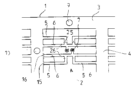
A substantially planar sheet 1 of an electrically conductive
metal such as a tin-bronze coated with silver is subjected to
a punching process whereby the configuration shown in Figs. 1
and 2 is formed. An array of sets of terminals generally
indicated by the reference number 2 are disposed in two
series of mutually orthogonal rows within the boundaries of
the sheet defined by narrow strips 3. Transverse strips 4
interconnect the strips 3 extending in the longitudinal
direction of the sheet 1 indicated by the arrow D.
Each of the sets 2 comprise four terminals 5 and four ter-
minals 6, each of the terminals 5 and 6 being at one end
thereof attached to a respective transverse strip 4. At their
opposite end, the terminals 5 and 6 are connected to each
other in pairs and are connected to a respective circular
contact nib 7 which in said punching process is formed such
that it projects out of the plane of the sheet 1.
After having been subjected to the punching process the sheet
1 is subjected to an injection moulding process in which an
array of fifteen by seven housings 8 of a plastic, electri-
cally insulating material are simultaneously moulded around
the terminals 5 and 6 of corresponding sets of same. One such
array is shown in Fig. 1.
CA 02224575 1997-12-12
WO 96/42097 PCTIDK96/00257
7
The sheet 1 has a length corresponding to a multiple of such
arrays and may comprise a small number of such arrays in case
it is desirable to work with a plurality of discrete sheets 1
in the various steps of the production process, and the sheet
1 may comprise a large number of such arrays in case it is
desirable to work with a continuous strip that may be wound
on a roll for transport between and feeding into the various
work stations or extend as a continuous strip between the
work stations in which the various production steps are
carried out. In all cases the sheet must be advanced to bring
a new area thereof into the work station and thereafter the
sheet must be fixedly positioned correctly in the work sta-
tion. Therefore, during the said punching process, apertures
9 and 10 are punched in the longitudinal strips 3 and the
transverse strips 4, respectively, the apertures 9 serving
primarily to advance the sheet and the apertures 10 serving
to position it.
After the housings 8 have been moulded around or unto the
sets 2 of terminals 5 and 6 the arrays are moved to a switch-
ing means installation work station either by transporting
discrete sheets 1 individually or in stacks to said work
station or by feeding a continuous sheet 1 into the work
station from the moulding station or via an intermediate roll
on which the continuous sheet 1 is wound.
In the said work station, fifteen moulded unitary push button
snap activating elements 11 are inserted substantially simul-
taneously in fifteen corresponding housings each from a
different longitudinal row in the sheet 1 but not necessarily
in the same transverse row. The activating element 11 con-
sists of a resiliently deformable material such as silicone
rubber. A contact element 12 consisting of a tin-bronze
coated with silver is partially embedded in the activating
element 11 during the moulding thereof. The unitary activat-
' -ing element 11 has an upper portion projecting upwards rela-
tive to the housing and intended to serve as a key element to
be depressed by the fingertip of a user of the switch. The
CA 02224575 1997-12-12
WO 96/42097 PCT/DK96/00257
8
dome shaped lower region of the activating element 11 allows
the contact element to be displaced from its inactive posi-
tion shown in Fig. 9 to its active position in which it is in
contact with both the contact nibs 7 when downward pressure ,
is applied to the upper region of the activating element 11.
The dome shape of said lower region entails a snap effect
when the downward pressure builds up sufficiently to overcome
the dome resistance so that a buckling of the dome shaped
lower region of the activating element 11 takes place
whereafter the contact element 12 electrically interconnects
the two contact nibs 7 immediately after the user has felt
the snap effect.
After the activating element 11 has been installed the sheet
is moved to a cover installation work station where a stain-
less steel cover 13 is arranged on the activating element 11
and is fixed to the housing by means of fastening members 14
that may be rivets, screws or projections of the housing
cooperating with corresponding apertures in the cover 13 and
the activating element 11, the fastening members 14 securing
the activating element 11 relative to the housing 8. This
step is also carried out substantially simultaneously on
fifteen switches, one from each longitudinal row of the sheet
1.
In a subsequent terminal separation work station the ter-
urinals 5 and 6 are separated from the sheet 1 at points
indicated by dotted lines 15 and 16, respectively, thereby
separating the completed switches from the sheet 1 and each
other. Depending on the application of the switch, i.e.
whether the application corresponds to utilization of the
terminals 5 (Figs. 3 - 5) or the terminals 6 (Figs. 6 - 8),
the outer portion of the terminals 6 or 5, respectively, are
separated from the switch at points indicated by dotted lines
26 and 25, respectively. '
CA 02224575 1997-12-12
WO 96/42097 PCT/DK96/00257
9
The terminals 5 or 6 may be bent to the required shape as
shown in Figs. 3 - 8 in a bending work station included in
the terminal separation work station such that the terminals
not relevant for the application in question are not separ-
ated from the sheet 1 until after the relevant terminals have
been separated from the sheet 1 and have been bent into the
correct shape in the bending work station.
These final steps are each also carried out substantially
simultaneously on fifteen switches one each from each longi-
tudinal row.
Naturally, a different number of simultaneously processed
switches can be chosen for the different manufacturing steps
depending on the methods chosen for performing the activities
comprised by the steps.
Example
The sheet 1 consists of silver plated tin-bronze with a
thickness of 0.35 mm. The outer portions of the terminals 5
and 6 are 0.6 mm wide and the distance from the bottom of the
housing 8 to the ends of the terminals 5 and 6 in Figs. 4 and
7, respectively, is 3.6 mm while the distance between said
ends in the same Figures is 4.5 mm. The distance between said
ends of the terminals 5 in Fig. 5 is 6.5 mm while the dis-
tance between the ends of the terminals 6 in Fig. 8 is 2.55
mm. The total height of the switch from the bottom of the
housing 8 to the top of the activating element 11 is 4.3 mm.
The diameter of the top of the activating element 11 is 2 mm.
The contact element 12 consists of silver plated tin-bronze
and the distance from its lowest portion in Fig. 9 to the top
of the contact nibs 7 is 0.7 mm. The activating element 11
consists of silicone rubber. The housing consists of PPS and
has outer dimensions of 4 mm by 4 mm in Figs. 3 and 6.
" The method according to the invention can be employed for a
variety of other types of switches such as rotary switches,
toggle switches, on-off switches etc. where a housing is
CA 02224575 1997-12-12
WO 96/42097 PCT/DK96/00257
attached to a set of terminals and switching means are
installed in and/or on the housing. The method can also be
employed in a variety of cases where the same basic switch
has different applications requiring different geometrical
5 configurations of the terminals, different widths and thereby
electrical resistances and so on. The number of sub-sets and
thereby different applications may be more than two. It would
be obvious to those skilled in the art how to apply the
principles of the invention to a series of technical problems
10 of this type.
Similar observations are valid with respect to the switch
according to the invention as the principles of said switch
can be applied to a variety of other types of switches such
as rotary switches, toggle switches, on-off switches etc. The
switch according to the invention can also be employed in a
variety of cases where the same basic switch has different
applications requiring different geometrical configurations
of the terminals, different widths and thereby electrical
resistances and so on. The amount of sub-sets and thereby
different applications may be more than two.
The method according to the invention is the more advan-
tageous the more different manufacturing steps are to be
performed when producing a particular switch.
Although the keyboard switch housing described with reference
to the drawings has a square cross section in a plane paral-
lel to the plane of the sheet, the same principles of the
invention will apply to such a switch with any other suitable
cross section shape, for instance circular, rectangular and
so on. Naturally, said keyboard switch or other switches
having multiple uses may also be manufactured in processes
utilizing per se known methods, for instance one switch at a
time or one row of switches from a narrow strip of conductive
material. '