Note: Descriptions are shown in the official language in which they were submitted.
CA 02225422 1997-12-22
WO 97/07539 PCT/FR96/01034
Laser surface treatment device and method
The invention relates to laser surface treatment, and
monitoring thereof.
It finds a particular application in the annealing of
amorphous silicon samples by excimer laser.
In general terms, the purpose of applying a laser beam to a
surface is to modify said surface, its structure and its
state.
In practice, the mechanism used is a partial fusion of the
surface, in the case of the crystallisation of amorphous
silicon.
The Applicant posed itself the problem bf providing a
device and method capable of monitoring, in real time, on
site, rapidly and non-destructively, a laser surface
treatment in which there are at least two generally similar
surface fields to be treated, of a given depth, to each of
which there is to be applied, on one or more occasions, a
treatment laser beam, with characteristics chosen so as to
change the physical state of each surface field.
The present invention affords a solution to this problem.
According to a general definition of the invention, the
method is characterised by the fact that it effects at
least one ellipsometry measurement before at least one of
the applications of the treatment beam to the second
surface field, in at least one area of the first surface
field, in order to obtain a characterisation of said first
surface field, the application of the laser beams and the
ellipsometry measurement being performed under generally
similar working conditions, which makes it possible to
CA 02225422 1997-12-22
2
monitor in real time, on site, non-destructively and
rapidly, the change in physical field state of each surface
field by means of said characterisation.
According to one embodiment of the invention, the
ellipsometry measurement is spectroscopic.
According to another embodiment of the invention, the
ellipsometry measurement is performed at one or several
wavelengths.
The optical analysis known as "spectroscopic ellipsometry",
normally used in the field of research and development, is
known. This type of analysis allows the characterisation
of a single layer or multilayer stack in a relatively wide
range of thicknesses.
It would there be theoretically possible to use such an
optical analysis for monitoring the change in physical
state of a surface obtained by laser. However, amongst
other factors, the complexity, the cost of such an
analysis, the time required and the size of the laser and
ellipsometer, mean that persons skilled in the art have not
until present thought of using it in this application,
industrially.
The Applicant observed that it is possible to arrange for
the analysis field of the ellipsometer to substantially
cover (in depth, but at a point) the three-dimensional
surface field (often referred to hereinafter as the
"surface", in order to simplify) affected by the impact of
the laser beam. This opens numerous possibilities for
monitoring the treatment of the different layers of said
surface. In addition, it =was observed that this analysis
and the laser treatment can be implemented under generally
similar working conditions by metrology and/or optical
means which are relatively simple and inexpensive, which
CA 02225422 1997-12-22
3
facilitates the obtaining of a reduced bulk, and also helps
to reduce the costs of implementing the method and device
of the invention.
In addition, the Applicant observed that the iriterval of
time between two applications of a high-power laser beam
makes it possible to effect at least one ellipsometry
measurement between the said laser applications.
The Applicant also observed that physico-chemical
characterisation by ellipsometry not only allows
monitoring, carried out before and/or after the laser
treatment, but also the optimisation of at least some of
the parameters of said laser treatment.
According to the invention, this optimisation of the laser
treatment takes place according to a predetermined law
dependant at least partly on said physico-chemical
characterisation, before, during or after each step of the
laser treatment.
In practice, one of the parameters of the optimisation of
the laser treatment is the energy applied by the laser beam
per unit surface and/or per unit time.
For example, the optimisation of the laser treatment
consists of adjusting the energy per unit surface and/or
per unit time afforded by the laser source in order to
obtain a laser beam appropriate to the surface field to be
treated, in accordance with the characterisation of this
field obtained by spectroscopic ellipsometry. More
precisely, this adjustment consists of varying the energy
of the laser beam, optically and/or mechanically and/or
electrically.
Another object of the invention is a treatment device for
implementing the method described above.
,
CA 02225422 2006-04-21
3a
In accordance with a first broad aspect of the present
invention, there is provided a laser surface treatment
method in which a series of at least two distinct zones are
employed that are substantially identical as regards
physico-chemical properties and each comprising a silicon
layer of given depth, and to each of which there is to be
applied, once or several times, a laser beam of energy
chosen so as to recrystalise the silicon layer of the said
zones, the method comprising the following steps:
a) carrying out, before at least one of the
applications of the laser beam to the first zone, at least
one ellipsometry measurement on the said first zone so as to
obtain a set of physico-chemical characteristics of the said
first zone.
b) determining the energy of the laser beam necessary
for the recrystallisation of the silicon layer of the first
zone, as a function of at least the set of characteristics
obtained in step a) and of a stored correspondence table,
c) subjecting the first zone to at least one pulse of
laser energy of magnitude determined in step b),
d) positioning the second zone with respect to the
laser beam, and
e) subjecting the second zone to at least one pulse of
laser energy of magnitude determined in step b), which
enables the process of recrystallisation of silicon by laser
on the said series of zones to be optimised by controlling
the application of the laser energy with the aid of the
ellipsometry measurement.
CA 02225422 2006-04-21
3b
In accordance with a second broad aspect of the present
invention, there is.provided a device for laser surface
treatment, for implementing the above referenced method in
which there is a series of at least two distinct zones,
substantially similar from the physico-chemical point of
view and each comprising a layer of silicon, of given depth,
and on each of which there is to be applied, on one or more
occasions, a laser beam with an energy chosen for
recrystallising the layer of silicon in said zones, said
device comprising an ellipsometer (EL) suitable for
effecting, before at least one of the applications of the
laser beam to the first zone, at least one ellipsometry
measurement on said first zone, in order to obtain a
multiplet of physico-chemical characteristics of said first
zone, calculation means (GES1, GES2) for determining the
energy of the laser beam necessary for the recrystallisation
of the layer of silicon in the first zone, as a function at
least of the multiplet of characteristics thus obtained and
a look-up table stored to memory, means (LA) for effecting,
on the first zone, at least one laser firing with an energy
thus determined by the calculation means, means (TAB) for
positioning the following zone opposite the laser beam, the
means (LA) being suitable for effecting, on the second zone,
at least one laser firing with an energy determined by the
calculation means on the first zone, which makes it possible
to optimise the process of recrystallisation of the silicon
by laser on said series of zones to be treated by
controlling the application of the laser energy by means of
the ellipsometry measurement.
CA 02225422 1997-12-22
4
Other characteristics and advantages of the invention will
emerge in the light of the description and drawings in
which:
- Figure 1 is an outline diagram of the installation for
monitoring the annealing of amorphous silicon panels by
excimer laser, according to the invention;
- Figure 2 is a schematic representation of a spectroscopic
ellipsometer associated with a surface treatment by excimer
laser according to the invention;
- Figure 3 depicts crystallinity curves of the laser
annealing of several types of sample (with or without non-
reflecting layer) performed at room temperature or at 240 C
according to the invention; and
- Figure 4 is a flow diagram illustrating the functioning
of the monitoring of the annealing of amorphous silicon
panels by excimer laser according to the invention.
The following description is based, non-limitatively, on a
particular application of the present invention which
concerns the manufacture of liquid crystal screens with an
active matrix, also referred to as AMLCD for "Active Matrix
Liquid Crystal Displays", and more precisely the step which
consists of manufacturing polysilicon transistors
(polysilicon thin film transistor, TFT), necessary both for
producing the screen control circuits and the display
elements.
The step of manufacturing the transistors determines the
performance of the screens, notably the display speed,
which is directly proportional to the speed at which the
screen control circuits are capable of working and
therefore to the mobility of the electrical charge carriers
in the material making up the TFT transistors.
CA 02225422 2006-04-21
The problem posed by the manufacture of polysilicon
transistors on large glass substrates is the processing
temperature, which must never exceed the critical
temperature of the substrate beyond which it loses its
5 properties (essentially mechanical). This temperature is
around 600 C for normal glass substrates (593 C for CORNINGTM
glass reference 7059 F for example).
However, at the present time, it is not known how to
deposit polysilicon directly at this temperature. The only
known solution consists of depositing a layer of amorphous
silicon and recrystallising it by adding energy to the
layer itself without exceeding the substrate destruction
temperature. The spontaneous crystallisation of the
amorphous silicon occurs, at temperatures of around 900 C.
It is a question therefore of transmitting sufficient
energy to the layer without excessively raising the
temperature of the substrate.
A first known solution consists of performing a heat
annealing of long duration. More precisely, it is a
question of keeping the panels, under a controlled
atmosphere, at a temperature just below the substrate
degradation temperature (typically 600 C), for several
hours. For example, after twelve hours of annealing,
crystallisation in solid phase is obtained. However, such
a technique has the drawback of offering limited production
capacity. In addition, the performance of the polysilicon
thus produced is not optimal in terms of mobility and
leakage current of the transistors which will be created
thereafter, probably because the solid-phase
crystallisation is never complete here.
Another known solution consists of using the technique
known as "rapid thermal annealing", also referred to as
RTP, standing for "Rapid Thermal Processing". It is a
question of effecting a rapid thermal annealing at high
CA 02225422 1997-12-22
6
temperature whilst limiting the heating of the substrate as
far as possible whilst promoting the temperature rise of
the amorphous silicon layer. For example, this preheating
is obtained by an array of infrared lamps disposed in the
vicinity of the panels. Constantly kept in movement, the
panels are preheated to 500 C, under a nitrogen atmosphere
at atmospheric pressure, by the array of infrared lamps,
whose energy is absorbed by the glass. This preheating
reduces the thermal shock produced by a light beam
generated by a high-energy xenon lamp, whose energy is
preferentially absorbed by the layer of silicon. This
additional heating, up to a temperature of around 750 C, is
localised on a strip approximately 1 cm wide on the
substrate by means of a sophisticated optical focusing
system.
Even if this method is fast, the homogeneity of the
treatment is however difficult to control, especially on
large surfaces. In addition, the properties of the
substrate can be degraded by an excessively high increase
in temperature, due to thermal diffusion.
Finally, a third known solution consists of exploiting the
particularly strong absorption of silicon in the
ultraviolet region, whilst glass is completely transparent
to the same wavelengths. It is a case then of using a
pulsed laser beam of high power, making it possible to
selectively raise the temperature of the layer of amorphous
silicon to melting point, without effecting the substrate.
The method has the advantage of being able to be carried
out very rapidly (the mean. duration of a pulse of an
excimer laser at 308 nanometres is generally less than 200
nanoseconds). As a result the interference effects of
heating of the substrate by thermal conduction are
negligible. In addition, the treatment is applied at room
CA 02225422 1997-12-22
7
temperature without any special precautions (at atmospheric
pressure).
In addition, a treatment limited to certain areas of the
panel is here possible, which makes it possible to envisage
a hybrid technology on both amorphous silicon and
polysilicon.
However such a technology is tricky on two points: it is
necessary to provide homogeneous treatment over large
surfaces, and it is necessary to completely control the
physical process of fusion/solidification by laser pulses.
In order to seek to ensure a homogeneous treatment over
large surfaces, it is known to use an excimer laser of
medium power (500 mJ in pulses), and to sweep the surface
of the sample to be treated by a series of laser impacts of
very small width (1 m). The lines thus swept overlap
partially and thus cover, by degrees, the entire surface
needed to be illuminated.
However, this solution has the drawback of requiring
thousands of laser impacts on a single substrate, and
therefore a high rate of operation of the laser (at least
500 Hz) in order to obtain a reasonable total operating
time. This rate is critical for the maintenance and
service life of the equipment, in particular the consumable
components.
In order to seek to provide a homogeneous treatment over
large surfaces, it is also known to use a high-power
excimer laser, for example an excimer laser with pre-
ionisation by X-rays supplying an effective power of 1 kW
(10 J x 100 Hz or 13 J x 80 Hz). This type of laser makes
it possible to obtain a high-power laser beam with a lower
repetition rate than the one previously described, which
CA 02225422 1997-12-22
8
allows treatment over a large surface, even up to the
entire surface of each panel, in a single laser pulse.
The remainder is placed in this context. As already
indicated, "surface field" refers to the whole of the
sample part to be treated; "zone" refers to the part of
this field treated in one pass of the laser. In addition,
"two generally similar surface fields to be treated" means
two surface fields which belong either to two separate
panels, which are generally similar; or to the same panel.
This problem, consisting of perfectly controlling the
physical process of fusion/crystallisation by laser pulses
on at least two generally similar surface fields is
resolved according to the invention by a method which
comprises at least one ellipsometry measurement performed
at at least one zone of the first surface field (at one or
more wavelengths, or else spectroscopic) before the
treatment of the second surface field by laser, in order to
obtain a physico-chemical characterisation of the first
surface field, and a monitoring in real time, on site,
which is non-destructive and rapid, of the laser surface
treatment by means of said characterisation.
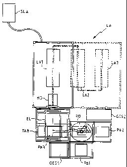
With reference to Figure 1, the device implementing the
method according to the invention comprises a laser source
LA having a power supply SLA and a plurality of excimer
laser heads, individualised at LA1 to LA3. The laser heads
are of high power and are positioned so as to produce a
single laser beam of very high power, for example 45 J.
The head LA1 is depicted in bold lines whilst the heads LA2
and LA3 are depicted in broken lines since they are
optional. The laser source or sources are of the XeCl
type, with a wavelength of 308 nm, for example.
This laser source is described in the patent application
entitled "Method and device for controlling a laser source
CA 02225422 2006-04-21
9
with several laser units in order to optimise laser surface
treatment", filed by the Applicant on the same date as the
present application under the number 95 09780.
Highly advantageously, the laser beam is adapted to the
desired zone size and at the same time homogenised by a
micro-lens device HO described in detail in the patent
application entitled "Optical device for homogenising a
laser beam", filed by the Applicant on the same date as the
present application under the number 95 09781.
The installation is completed by an electronic management
system GES1 and GES2 controlling a robot RO which moves the
panels, a table TAB with x, y and z axes, and an
ellipsometer EL, which can be spectroscopic. This
ellipsometer EL can effect both the monitoring of the
positioning of the panels with respect to the laser beam,
and the real-time monitoring of the development of the
laser treatment of the panels.
Spectroscopic ellipsometry is a non-destructive optical
method of characterisation of multilayer stacks, applicable
in a layer with a fairly large thickness, ranging for
example from 0.1 nanometres to 10 m.
The measurement is based on the variation in polarisation
of a beam of light after reflection on the surface of the
sample to be analysed. The thicknesses are arrived at by
considering the contrast in indices between layers of
different materials.
Advantageously, the physico-chemical characterisation of
the surface field comprises the measurement of at least one
CA 02225422 1997-12-22
of the parameters belonging to the group formed by the
thickness of this field, the density and the optical index
of this field, the thickness of the different layers
constituting the surface, and the physico-chemical
5 composition of this field. The set of quantities measured,
for a given application, can be referred to as the
"multiplet of physico-chemical characteristics".
With reference to Figure 2, the reference EL designates a
10 spectroscopic ellipsometer, for example the one sold by the
Applicant under the commercial references ES4G, MLM, or
GESPS. Such an ellipsometer is described, at least in
principle, for example in French patent No 8603188
published as FR-A-2 595 471.
A power supply 1 excites a light source 2, such as a high-
pressure xenon arc lamp. A first optical system 10,
including means 15 able to act on the polarisation,
transforms the light beam coming from the source 2 into a
beam which strikes a panel PA mounted on the table TAB,
preferably movable in three directions orthogonal to each
other X, Y and Z.
The useful light is that reflected by the panel,
symmetrically with the incident beam with respect to a
normal to the surface of the panel.
This reflected light is taken up by a second optical system
20 comprising an analyser 25, in order to be applied to the
entrance slot of a prism monochromator 6. The light coming
from the exit slot of the monochromator 6 is applied to a
photodetector 7 comprising an array of photodiodes, for
example 512 or 1024 pixels, making it possible to effect
the wavelength detection (or else a single-way
photodetector, in the case of a non-spectroscopic
ellipsometer).
CA 02225422 1997-12-22
11
An electronic control unit GES1 acts:
- on the polarisation means 15, in order to control its
effects on the polarisation of the incident light (in the
presence of polarisation means of the rotary polariser
type, the electronic control unit acts on the continual
setting in rotation of the polariser),
- on the table TAB, in order to control its positioning
with respect to X-Y-Z,
- on the robot ROB in order to control first of all the
extraction of a panel to be treated from the storage rack
in which the panels to be treated are stored, then the
movement of the panel thus extracted to the table, then the
positioning of the said panel on the table at a chosen
location and, after the ellipsometry (at one or more
locations), the gripping of the panel in order to replace
it in the initial storage rack or in another storage rack,
- on the analyser 25, in order to control its orientation
through a stepping motor,
- on the monochromator 6, in order to define its tuning
wavelength,
- on the laser source LA, in order to control its flux
according to the invention.
The signal coming from the photodetector 7 is applied to
the management means GES1 in order to be recorded in
connection with the state of polarisation of the incident
light (for example, the angle of the polariser 15 in the
case of a rotary polariser), and other data collected,
including notably the position of the panel to be treated,
that of the analyser and the wavelength to which each
measurement corresponds.
CA 02225422 1997-12-22
12
This information, optionally pre-processed by the
electronic unit GESl, is transmitted to processing means
GES2, such as a microcomputer, which derives therefrom the
ellipsometry information (for example "tangent psi" and
"cosine delta"), then curves representing the surface state
and/or the multilayer structure of the panel to be treated,
as a function of each impact position of the ellipsometry
analysis spot.
A chassis, preferably a single one, comprises the power
supply 1 of the xenon lamp 2, the management means GES1,
the monochromator 6, the detector 7 and if applicable the
processing means GES2.
In practice, the light radiation of the source 2 is
transmitted by a lens 30 to the entrance coupler 31 of an
optical fibre 3. This joins the optical system 10, which
comprises a fibre exit coupler 11, a lens 12, a collimation
diaphragm 13, and the polariser 15.
The parallel beam from the polariser 15 is focused by a
convergent lens Ll on a focal point PF of the panel to be
treated. The lens Li is disposed at the object plane of
the panel.
The reflected radiation is focused by another convergent
lens L2 on the entrance coupler 27 of the second optical
fibre S. The lens L2 is disposed at the image plane of the
panel. The lenses Li and L2 are optically connected.
The exit coupler 28 of the optical fibre 5 delivers a
radiation taken up by a lens 29 so as to be applied to the
entrance slot of the monochromator 6.
The detector 7 is opposite the exit slot of the
monochromator.
CA 02225422 2006-04-21
13
The optical assembly consisting of the lenses L1 and L2
eliminates the interference reflection caused routinely by
the rear face of a sample comprising a glass substrate with
a large thickness.
This mechanical elimination of the contribution of the rear
face of the sample is described in detail in the patent
application entitled "Ellipsometer device with high spatial
resolution", filed by the Applicant on the same date as the
present application under the No 95 09779.
In addition, the error in positioning the wafers on the Z
axis is critical because of the spatial resolution of the
spot. This positioning error is corrected as follows.
Firstly, the curvature of each type of panel in the
vertical direction Z is taken into account by making an
adjustment, manual or other, of the ellipsometry spot.
After learning, this adjustment is stored to memory, for
the different zones of the panel intended to be analysed by
ellipsometry. In addition, the cartography of the profile
of each type of panel is stored to memory in the computer
GES2 (it is derived from the adjustments related to
curvature.
Secondly, in the remainder of the process of monitoring the
surface treatment, the positions of impacts thus adjusted
and stored are re-used at each analysis position. They can
also serve for a subsequent laser treatment.
However, this is not always sufficient since differences in
deformations can occur between panels of the same type.
CA 02225422 1997-12-22
14
A fine adjustment of the position of the spot on the exit
fibre 5 is obtained by rotating a transparent plate PT
disposed between the analyser 25 and the entrance coupler
of the optical fibre S. This rotation is controlled by the
S management means GESl so as always to be at the signal
maximum on the photodetector array 7.
This last solution is also described in the patent
application filed by the Applicant for an "Ellipsometer
device with high spatial resolution", mentioned above.
In annealing by single-pulse excimer laser, the laser pulse
FLA is of a very short duration, for example less than 200
nanoseconds. Such a pulse very rapidly supplies sufficient
energy to reach partial or total fusion of a layer of
amorphous silicon: the absorption of the laser beam being
complete after 0.2 microns penetration, the heating (with
recrystallisation) is first of all limited to the front
surface, namely the one receiving the laser impact; it next
extends to the whole of the layer, either by simple thermal
diffusion or by a so-called "explosive" crystallisation
phenomenon.
The energy threshold per unit surface needed to obtain the
fusion of the front surface of the layer of amorphous
silicon is here less than 400 mJ/cm2. Above this energy,
the layer of silicon is subject to a more extensive partial
fusion. At 500 mJ/cma, the fusion is total and the energy
added above this is a priori no longer useful for improving
recrystallisation. It can even be harmful, since the layer
of amorphous silicon can also melt with excessively high
absorption of energy, beyond 800 mJ/cm2.
This shows the advantage of obtaining, during laser
treatment, a characterisation of the structure of the
surface to be treated by ellipsometry, with a view to
optimising said laser surface treatment.
CA 02225422 1997-12-22
In addition, the quality of the polysilicon obtained
depends mainly on the size and arrangement of the grains of
the silicon, and therefore on the crystallisation process
itself.
5
However, the average size of the polysilicon crystals
obtained depends on the laser energy applied.
This is because the large crystals, which are the most
10 favourable to an optimum functioning of the device, are
obtained in a very narrow range of flux (or energy per unit
surface). This range corresponds to the operating
conditions of the laser, which make it possible to melt the
layer of amorphous silicon almost entirely, whilst
15 preserving a few unmelted grains of polysilicon. These
grains fulfil the role of crystallisation precursors in the
progressive recrystallisation of the melted layer and thus
promote the appearance of large crystals. On the other
hand, in the case of complete and/or free fusion of the
layer, these precursors disappear, and the size of the
grains obtained falls abruptly by one or two orders of
magnitude.
These observations on the critical character of the
crystallisation process highlight the interest and
advantages afforded by the present invention.
Advantageously, the monitoring method according to the
invention also comprises a step in which provision is made
for optimising at least some of the laser processing
parameters according to a predetermined law dependent at
least partly on the physico-chemical characterisation of
the surface obtained by ellipsometry measurement.
The essential parameters of the laser treatment to be
monitored from the teachings of the present invention are
the flux of the laser and the thickness of the layer of
CA 02225422 1997-12-22
16
amorphous silicon to be treated by laser. However, apart
from the laser flux and the initial thickness of the layer
of amorphous silicon, other parameters can act in the
monitoring process.
In some cases, the structure of the material to be annealed
can be more complex than a simple layer of amorphous
silicon on a glass substrate. This is a case when a
transparent layer is provided (at the laser emission
spectral band), where the judicious choice of its thickness
makes it possible, by simple optical effect, to
substantially increase the efficacy of the laser treatment.
For example, the use of a layer of glass of suitable
thickness, for example 48 nanometres, makes it possible to
increase the effective absorption of the layer of amorphous
silicon from 0.42 to 0.68, that is to say a gain in surface
area treated of approximately 50%- for an equal initial
energy. In addition, the use of a silicon Si3N4 glass
instead of a Si02 glass is even more favourable since the
gain in surface area treated is more than 100%-.
The counterpart of the presence of such a non-reflecting
layer is to make the process more complex and more
difficult to control, since the optimum influence will
depend also on the thickness of the non-reflecting layer,
and this in a critical fashion.
In addition, a preheating of the layer to be treated by a
conventional means at a reduced temperature, for example
250 to 400 C, advantageously makes it possible to
appreciably reduce the flux required for recrystallisation.
The sizes of the polycrystals obtained are slightly
increased. However, the process is then more critical than
when the laser treatment is carried out at room
temperature.
CA 02225422 1997-12-22
17
Advantageously, the monitoring method according to the
invention makes it possible effectively to monitor this
preheating step by means of ellipsometry measurements.
It should be noted that the amorphous silicon deposited by
low-temperature techniques, such as PECVD ("Plasma Enhanced
Chemical Vapor Deposition") is rarely free of hydrogen.
This is because the use of a mixture of silane-based gas
for depositing this type of layer results in the fact that
it is difficult to be rid of the hydrogen which is always
present in large quantities in the reactors as by-products
of the decomposition of the silane.
However, the treatment by excimer laser, without any
precaution, of a layer of amorphous silicon which is highly
contaminated with hydrogen, is generally catastrophic. The
abrupt release of hydrogen during the
fusion/crystallisation process generally leads to a
veritable explosion of the layer and/or to final surface
roughness, which is completely incompatible with the
desired performance.
In this case, one solution consists of effecting a
treatment in two steps. First of all, a low-energy impact
laser is first applied so as to release the hydrogen
without fusion, even partial, of the layer of amorphous
silicon. Next, the recrystallisation process is effected
during a second laser impact of higher power than the first
(its power is to be adjusted having regard to the effects
of the first laser impact).
The on-site monitoring method by spectroscopic ellipsometry
according to the invention here finds another advantageous
application in the treatment of a layer of silicon
contaminated with hydrogen.
CA 02225422 1997-12-22
18
Generally, a spectroscopic ellipsometry measurement before
laser annealing makes it possible to measure precisely,
according to the invention, the following parameters:
- the thickness of the layer of amorphous silicon: the
thickness used is situated between 30 and 80 nanometres.
In this range of thicknesses, the accuracy of the
ellipsometry is better than 0.5%,;
- the thickness of the non-reflecting layer: the accuracy
is comparable with or better than that obtained on the
layer of amorphous silicon;
- the optical index of the layer of amorphous silicon: the
presence of inserted hydrogen in the layer of_amorphous
silicon gives rise to a decrease in the optical indices
which is perfectly detectable in spectroscopic
ellipsometry.
The use of a spectroscopic ellipsometer before any
treatment makes it possible thus to obtain according to the
invention a complete image of the structure of the samples,
both in terms of thickness and with regard to the physico-
chemical composition of the layers of amorphous silicon.
In addition to the crystallinity of the layers, it is
possible to determine the roughness of the surfaces of the
samples. This is because the appearance of a surface
roughness (in particular after treatment) can be detected
since it causes a deformation of the ellipsometry curves
which is different from that caused by a variation in
thickness. This possibility is very important for
monitoring the panel manufacturing process described below.
The starting point is glass panels covered with a small
thickness of amorphous silicon which are substantially
identical, in particular of the same manufacture (the same
CA 02225422 1997-12-22
19
series). Preferably the annealing monitoring method
comprises initially a test procedure followed by an
annealing procedure proper.
The test procedure comprises the following steps:
1) - providing several test panels and effecting, for each
of them, an ellipsometry measurement at the positions of
the centres of the future laser impacts;
2) - providing a step of regression (or other statistical
processing) of the different measurements and evaluating
the average structure of the panels; it should be noted
that, in this application, the parameters which are most
particularly evaluated are the thicknesses of the layers,
the dielectric constants of the amorphous silicon and the
homogeneity of the panels for the amorphous silicon and the
non-reflective layer as appropriate;
3) - estimating the average energy of the laser needed for
the structure thus considered;
4) - treating several test panels with energies in the
range having a value of around 0.5 times the average energy
up to a value of around 1.5 times the said average value;
5) - where applicable, effecting an ellipsometry
measurement on the same panels after laser treatment;
advantageously, this is supplemented with a step of
regressing the measurements, and an evaluation of the
results, in order to determine the crystallinity as a
function of the energy of the laser, the exactitude of the
regressions (as a whole) and the presence of any roughness.
This test procedure results in a precise evaluation of the
optimum energy needed to crystallise the structure under
consideration. -In the ideal case, this evaluation can be
CA 02225422 1997-12-22
validated by a complementary physical measurement such as
resistivity, crystallinity by X-rays, notably.
According to the invention, the incident power of the laser
5 is adjusted either by direct action on the laser pulse or
by an energy variator such as an optical attenuator
(diaphragm, absorbent sheet), a variator for the supply
voltage of the laser source or for the distance between the
two collecting lenses of the homogenising optical device.
In the case of a simple amorphous silicon structure, for
example with a thickness of 45 nanometres and glass treated
at ambient temperature, the measurement by ellipsometry
before treatment gives a thickness of amorphous silicon of
45 nanometres with a variance of around 101; due to the
heterogeneity of the deposition. The presence of a thin
layer of native oxide on the surface, for example of around
2.2 nanometres, must be taken into account for a correct
adjustment of the measurements. The mean index of the
amorphous silicon specific to this type of sample is then
extracted and compared with the reference indices. In this
precise case, the index found is very close to that of a
dense amorphous silicon, and therefore not very liable to
contain a great deal of inserted hydrogen. A conventional
treatment including a single laser pulse can therefore be
optimised.
A certain number of samples are next annealed by laser with
fluxes variable in the range 250 to 370 mJ/cm2. These
samples are analysed by ellipsometry. By regression, using
the index of the previously extracted amorphous silicon,
the crystallinity of various samples is deduced.
The crystallinity curve Cl (Figure 3) shows the presence of
a highly marked crystallisation threshold at approximately
255 mJ/cmz. This is in fact the energy threshold necessary
for partial fusion of the layer of amorphous silicon at
CA 02225422 1997-12-22
21
room temperature. Below this threshold, the entire layer
of silicon appears partially crystallised. The
crystallisation rate increases progressively up to energies
sufficient for the whole of the layer to fuse. This change
is to be related to the description of the process given
previously. The optimum treatment is reached when the
crystallinity level measured by spectroscopic ellipsometry
is at a maximum, here 350 mJ/cm2. This optimum corresponds
to the best adjustment of the model to a simple homogeneous
layer, in the example chosen.
In another example (curve C3), the samples have a non-
reflective layer of silicon with a thickness of around 55
nanometres, deposited on the layer of amorphous silicon.
The optimisation process is effected in the same way as
before, and the energy range chosen is smaller because of
the presence of the non-reflective layer. The same type of
analysis after laser impact gives a crystallinity curve
similar to the previous one, but very appreciably offset
towards the low energies. The optimum energy is reduced to
approximately 260 mJ/cm2, which corresponds to the energy
gain introduced by simple optical effect.
It should be noted that monitoring by spectroscopic
ellipsometry is particularly interesting in the complex
case with a non-reflective layer. This technique also
gives precisely the thickness of the non-reflective layer.
In other applications, ellipsometry with one or several
wavelengths may suffice.
In addition, the same types of sample with and without non-
reflective layer have also been annealed by laser under
vacuum by raising the temperature of the substrate to
approximately 240 with impact. The same types of analyses
give results (curves C2 and C4) set out in Figure 3.
Compared with the results obtained at room temperature,
preheating the substrate again makes it possible to reduce
CA 02225422 1997-12-22
22
the optimum energy required for crystallisation by
approximately 50 mJ/cmz. The best results in terms of
crystallinity are apparently obtained at 240 C in the
presence of a non-reflective layer (curve C4). In
addition, the optimum energy needed is the lowest, below
240 mJ/cmz, which shows the interest of these parameters.
After the test procedure designed to optimise the energy of
the laser beam, the monitoring of the annealing proper can
be set up.
With reference to Figure 4, the method of monitoring the
laser annealing comprises the following steps (for each
laser impact on a panel):
- Step El: first ellipsometry measurement (duration of
around 1 sec, with adjustnient for height and fine setting,
as well as rapid acquisition);
- Step E2: regression and calculation of the laser energies
(duration of 0.5 secs);
- Step E3: adjustment of the laser energy (duration 1 sec);
- Step E4: laser firing;
- Step E5: where applicable, second ellipsometry
measurement (duration 1 sec);
- Step E6: movement of the panel to the following position;
- Step E7: regression and evaluation of crystallinity;
- Step E8, final treatment test; and
- Step E9: change of panel or wafer, and return to step El.
CA 02225422 1997-12-22
23
For example, the period of repetition of the laser impacts
is 6 secs and a panel of 40 x 30 cm is treated in 9 pulses,
that is to say a treatment capacity of around 50 panels per
hour, for the times indicated.
Thus the method described makes it possible not only to
improve the quality and reliability of the laser annealing
of amorphous silicon, but also to monitor a posteriori the
step of deposition of the amorphous silicon, whose
homogeneity is not always perfect.
In so far as, for example, it is possible to sacrifice
samples, as described above, the method described can be
implemented only after the laser surface treatment.
However, it is currently preferred for it also to be
carried out before this surface treatment, at least for
some applications. In other applications, it will only be
carried out before the laser surface treatment.
In its developed version, the method can be defined in
other terms as follows:
- a) effecting, before said laser surface treatment, at
least one ellipsometry measurement on one of the zones to
be treated of a panel immobilised in an initial position
defined by three coordinates relative to an orthonormed
reference frame (X, Y, Z), in order to obtain a multiplet
of physico-chemical characteristics on its surface;
- b) determining the energy of the laser beam necessary for
the treatment, as a function of at least the multiplet of
characteristics obtained at step a) and a look-up table
stored to memory,
- c) effecting a laser firing with an energy determined at
step b) in order to treat the surface of the zone,
CA 02225422 1997-12-22
24
- d) moving the panel in the plane XY so that another zone
is positioned opposite the laser beam, and
- e) recommencing the method at least at step c).
Better still, at step a), an ellipsometry measurement is
carried out on each zone to be treated on the panel, in
order to obtain the multiplet of physico-chemical
characteristics of the surface of each zone to be treated,
whilst at step b) the energy of the laser beam needed for
the treatment is determined according to all the multiplets
of characteristics obtained at step a).
As applicable, at step d), the positioning comprises a sub-
set dl) in which an ellipsometry measurement is effected on
the zone, in order to adjust its positioning according to
the direction Z.
According to a variant, between steps d) and e) an
intermediate step d') is provided in which the energy of
the laser needed for the surface treatment of the zone is
adjusted, according to the energy determined at step b),
the position adjustment effected at sub-step ol) and the
look-up table.
According to another variant, between steps c) and d), a
sub-step c') is provided in which an ellipsometry
measurement of the treated surface is effected, in order to
determine the new characteristics of the multiplet.
In its complete version, the method can be defined as
follows:
- a) performing an ellipsometry measurement on each zone to
be treated on a panel immobilised in an initial position,
before said laser surface treatment, in order to obtain a
CA 02225422 1997-12-22
multiplet of physico-chemical characteristics of the
surface to be treated on each zone,
- b) evaluating the mean energy of the laser necessary for
5 the mean surface treatment of the panel, as a function of
the characteristics obtained at step a) and a look-up table
stored to memory, and
next, for each zone to be treated:
- c) effecting a new ellipsometry measurement on the zone,
in order to adjust its positioning with respect to the
initial position,
- d) adjusting the energy of the laser needed for the
surface treatment of the zone, as a function of the mean
energy evaluated at step b), the position adjustment
effected at step c) and the look-up table, and
- e) effecting a laser firing with an energy determined at
step d) in order to treat the zone.
In all its presentations of method, the invention can also
be defined in the same way in the form of a corresponding
device, and vice versa.