Note: Descriptions are shown in the official language in which they were submitted.
CA 0222~7~1 1997-12-24
W~97/02S97 PCT~S95.
A MET~OD OF MAN~FACTURING A
MONOLITHIC T-TN~ OPTOCO~PLER
TEC~NICAL FIELD
5A related application entitled "A MONOLITHIC LINEAR
OPTOCOUPLER" by the same inventor, is being filed on the
same day herewith and is incorporated by reference herein.
The present invention relates to an optocoupler. The
present invention relates, in particular, to a method of
making a monolithic structure for an optocoupler that
provides improved linearity.
BACKGROUND OF THB lNV,'~l lON
Optocouplers are used to electrically isolate an input
signal from a corresponding output signal. For example,
optocouplers may be used in data access arrangements
("DAAs"). A data access arrangement (DAA) is used for
interfacing a data terminal equipment ("DTE") (such as data
modems, facsimile machines, non-cellular portable
telephones, speaker phones, and message answering machines,
~or example) with lines of the public switched telephone
network ("PSTN"). The network (PSTN) must be protected from
potential damage due to, for example, faulty data terminal
equipment (DTE) or inadvertent shorts through the data
t:erminal equipment (DTE) to its power line. Indeed, the
IJnited States Federal Communications Commission ("FCC")
recruires a 1500 volt isolation between data terminal
equipment (DTE) and the network (PSTN). In the past, data
~ccess arrangements (DAAs) have used transformers to
provide such electrical isolation. However, due to their
relative expense and large size and weight, transformers
are disadvantageous, particularly for use in portable data
t:erminal equipment (DTE). Alternative isolation
components, such as optical isolators, must be used for
siuch reduced volume/weight applications.
Known optocouplers include an LED which is optically
coupleable with, but electrically isolated from, a
CA 0222~7~1 1997-12-24
W097/02S97 ~CT~S96/04975
photodiode. The photodiode ("the output signal photodiode")
generates an output signal based on the intensity of light
emitted from the LED and detected by it.
Known optocouplers may also include an additional
photodiode ("the feedback control signal photodiode") for
generating a servo-feedback signal based on the intensity
of light emitted from the LED and detected by it. The
feedback control signal photodiode allows the optocoupler
to operate more linearly. In these known optocouplers, the
output signal photodiode and the feedback control signal
photodiode are discrete elements. As such, a first
direction defined between the LED and the output signal
photodiode differs from a second direction defined between
the LED and the feedback control signal diode.
Unfortunately, the LED may emit directionally non-uniform
light. As a result, the intensity of light detected by the
output signal diode usually varies from the intensity of
light detected by the feedback control signal diode.
Consequently, the output of the feedback control signal
photodiode will not accurately indicate the intensity of
the light from the LED detected by the output signal
photodiode, thereby preventing the full compensation of
non-linearities in the operation of the optocoupler.
One solution to the problem of directionally
non-uniform light emission is to place the output signal
photodiode in close proximity to the feedback control
signal photodiode. Unfortunately, this offers only a
partial solution because directionally non-uniform light
will still cause non-linearities, although to a lesser
extent. In addition, the feedback control signal photodiode
must be adequately isolated from the output signal
photodiode to provide adequate electrical isolation. Such
isolation is difficult when the two photodiodes are located
close to one another.
In view of the above described problems with known
optocoupler circuits, an optocoupler immune to
directionally non-uniform light emission by the LED is
.
CA 0222~7~1 1997-12-24
PCT/US96/04975
WC~ 97/02597
needed. Furthermore, any photodiodes of the optocoupler
should be ade~uately electrically isolated from one
i~nother. Moreover, the optocoupler should be relatively
r l~imple and economical to manufacture. If possible, the
5 optocoupler should be integrated on a single chip.
~UMMARY OF THE l~.v~ ON
Briefly, the present invention provides a method for
i.abricating a monolithic semiconductor device, comprising
10 c;teps of forming trenches in the top surface of a silicon
wafer; forming an N+ region on the top surface of the wafer
and the inner surfaces of the trenches; forming a first
oxide layer on the N+ region; removing the silicon wafer
such that portions of the N+ region are exposed; forming P+
15 regions that cover the exposed portions of the N+ region;
adding a second oxide layer on the P+ regions; and adding
a substrate on the second oxide layer.
The step of forming P+ regions may include forming a
20 first photodiode having a cathode and an anode, and a
second photodiode having a cathode and an anode.
The method may also include providing electrical
connections to the cathodes and anodes of the first and
25 second photodiodes. The method may also include forming a
light emitting diode on the upper surface of the device.
A reflective dome may be provided above the monolithic
st:ructure thereby forming an optical cavity. The
30 re!flective dome increases the signal to noise ratio of the
optocoupler.
BRIEF DESCRIPTION OF THE DR~INGS
For a better understanding of the invention, reference
35 is made to the following description of an exemplary
embodiment thereof, and to the accompanying drawings,
wherein:
CA 0222~7~1 1997-12-24
WO 97/02597 PCT/US~5/., 1~7:~
Figure 1 is a side view, through the cross-section
defined by line I-I of Figure 2, of an optocoupler
constructed in accordance with the present invention;
Figure 2 is a plan view, through a cross section
defined ~y line II-II shown in Figure 1, of the optocoupler
of Figure l;
Figure 3 is a schematic diagram of a conventional
optocoupler chip having an externally coupled feedback
control loop; and
Figures 4a through 4d illustrate a method for
fabricating the monolithic structure of an optocoupler of
the present invention.
D~TAIL~D DE8CRIPTION
Figure 3 is a schematic diagram of a conventional
optocoupler chip 390 having an externally coupled feedback
control loop. The conventional optocoupler includes a
LED 300, an output signal photodiode 310, and a feedback
control signal photodiode 320. A differential (error)
operational amplifier 330 is coupled from a control signal
output terminal 394 to a LED input signal terminal 391.
The LED 300 emits a light having an intensity based on
the voltage of a signal output from the differential
amplifier 330. ~he differential amplifier 330 may either
source or sink the LED current. The output signal
photodiode 310 is electrically isolated from, and optically
coupleable with, the LED 300. A first direction Dl is
defined from the LED 300 to the output signal
photodiode 310. The anode of the output signal
photodiode 310 is coupled with a first voltage source Vs1
via terminal 395 and the cathode of the output signal
photodiode 310 is coupled with an output load via
terminal 396. Alternatively, if a depletion layer
photodiode is used, the cathode of the output signal
photodiode 310 can be coupled with a voltage source and the
anode of the output signal photodiode 310 can be coupled
- - -
CA 0222~7~1 1997-12-24
PCT/U~ 7a
W~ 97~2597
with the output load, such that the reverse biased
depletion layer photodiode operates below its breakdown
voltage. In either case, the output signal photodiode 310
supplies an output signal to the output load (or to an
output driver) based on the intensity of light detected by
it.
The feedback control signal photodiode 320 is also
op~ically coupleable with the LED 300. Although the
feedback control signal photodiode 320 may also be
electrically isolated from the LED 300, such electrical
isolation is not required. A second direction D2 is
defined from the LED 300 to the feedback control signal
photodiode 320. The anode of the feedback control signal
photodiode 320 is coupled with a second supply voltage Vsz
via terminal 393 and the cathode of the feedback control
signal photodiode 320 is coupled with a first (inverting)
input of the differential amplifier 330. Alternatively, if
a depletion layer photodiode is used, the cathode of the
~eedback control signal photodiode 320 can be coupled with
a voltage source and the anode of the feedback control
signal photodiode 320 can be coupled with the first input
of the differential amplifier 330, such that the reverse
biased depletion layer photodiode operates below its
breakdown voltage. A second (non-inverting) input of the
cLifferential amplifier 330 is provided with an input signal
~ DP~IVE '
Unfortunately, the LED 300 does not emit light in a
directionally uniform manner. Consequently, the intensity
cf the light emitted in direction Dl may vary from the
intensity of the light emitted in the direction D2. This
difference in detected intensity makes it difficult to
properly control the voltage applied to the LED 300. As
discussed above, if the output signal photodiode 310 is
placed in close proximity to the feedback control signal
photodiode 320 such that the direction D1 closely
approaches the direction D2, electrically isolating the two
photodiodes may become difficult.
CA 0222~7~1 1997-12-24
PCT~S96/04975
W097/02597
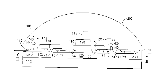
Figure 1 is a cross-sectional side view of the
monolithic structure 100 of an optocoupler of the present
invention. The cross section is taken across a middle of
the monolithic structure as shown by line I-I of Figure 2.
The monolithic structure lOo includes a silicon
substrate 110, a layer of oxide 120 (such as silicon
dioxide for example), an inner silicon section 160, an
inner silicon tub 150, an outer silicon tub 140, a thick
oxide (such as silicon dioxide) covering 130, and a light
emitting diode (LED) 190.
The layer of oxide 120 is located above the silicon
substrate llo such that an interface is defined between an
upper surface of the silicon substrate 110 and a lower
surface of the oxide layer 120. The inner silicon section
160 is located on, and preferably in a center region of, an
upper surface of the oxide layer 120. The inner silicon
tub 150 is located on the upper surface of the oxide layer
120 and surrounds the inner silicon section 160. The inner
edges 159 of the inner silicon tub 150 are spaced from the
outer edges 168 of the inner silicon section 160 thereby
defining an first area 56 of the upper surface of the oxide
layer 120 that is not in contact with a silicon structure.
The outer silicon tub 140 is located on the upper surface
of the oxide layer 120 and surrounds the inner silicon tub
150. The inner edges 149 of the outer silicon tub 140 are
spaced from the outer edges 158 of the inner silicon tub
150 thereby defining a second area 45 of the upper surface
of the oxide layer 120 that is not in contact with a
silicon structure.
The inner silicon tub 150 includes a rectangular
p-doped "tub" region 151. Alternatively, the silicon
tub 150 may have an octagonal p-doped "tub" region 151.
Providing an octagonal p-doped "tub" region 151, however,
requires an additional step of etching corner regions
during fabrication. Indeed, the shape of the p-doped "tub"
region 151 may assume any shape that surrounds the LED 190
and that can be fabricated from the crystalline structure.
CA 0222~7~1 1997-12-24
w~g7l02ss? PCT~S3fl~
~lowever, symmetric shapes, and in particular, shapes
symmetric with respect to two perpendicular lines
~ntersecting at the center of the shape are preferred.
An n-doped region 152 is located within the p-doped
t:ub 151 thereby forming a p-n junction 151-lS2. This p-n
~unction 151-152 defines a first diode; the p-doped tub 151
forming the anode of the first diode and the n-doped
region 152 forming the cathode of the first diode.
Similarly, the outer silicon tub 140 includes a rectangular
p-doped "tub" region 141 but can assume other shapes (such
as octagonal) as discussed above. An n-doped region 142 is
located within the p-doped tub 141 thereby forming a p-n
junction 141-142. This p-n junction 141-142 defines a
second diode; the p-doped tub 141 forming the anode of the
second diode and the n-doped region 142 forming the cathode
of the second diode.
The thick oxide covering 130 covers the inner silicon
region 160, the inner silicon tub 150, the outer silicon
tub 140, and the first and second areas 56 and 45 of the
upper surface of the oxide layer 120 not covered with
silicon. However, voids for providing access to cathode
(144,154) and anode (145,155) bond pads are formed in the
t.hick oxide layer to permit anode and cathode connections
to be formed to the first and second diodes. Specifically,
a; shown in Figures 1 and 2, the void 145 provides access
to a cathode bond pad on the n-doped region 142 of the
outer silicon tub 140. A similar void 144 provides access
to an anode bond pad on the p-doped tub 141 of the outer
s:ilicon tub 140. Similarly, as shown in Figures 1 and 2,
the void 155 provides access to a cathode bond pad on the
n--doped region 152 of the inner silicon tub 150. A similar
void 154 provides access to an anode bond pad on the
p-doped tub 151 of the inner silicon tub 150.
The LED 190 is arranged on an upper exposed surface of
the thick oxide covering 130. As shown in Figure 2, the
~D 190 includes a cathode bonding pad 194 and an anode
bonding pad 195. The thick oxide covering 130 should
CA 0222~7~1 1997-12-24
WO 97102S97 PCT/US9~ J
permit light at the wavelength of the light (typically
infra-red) emitted by the LED 190 to pass. That is, the
thick oxide covering 130 should be substantially
transparent to light emitted by the LED 190.
An optional reflective dome 200, covering the
monolithic structure 100, may also be provided. The
reflective dome 200 may be made from an optically
transparent material having a reflective layer for example.
The first diode 151,152 formed by the inner silicon
10 tub 150 is a photodiode and may be used to either generate
an output signal or a feedback control signal. However,
given its close proximity to the LED 190, the first
photodiode 151, 152 is preferably used for generating a
feedback control signal for the LED l9o. This is because
15 the feedback control signal photodiode does not need to be
electrically isolated from the LED 190. The second
diode 141, 142 formed by the outer silicon tub 140 is a
photodiode and may be used to either generate a feedback
control signal or an output signal. The second
20 photodiode 141, 142 should perform the function not being
performed by the first photodiode 151, 152. Accordingly,
the second photodiode is preferably used for generating an
output signal. This provides even better electrical
isolation between the output signal photodiode and the
25 LED 190.
In operation, when the LED 190 emits light, some of
the emitted light passes through the optically transparent
thick oxide layer 130 to the first and second photodiodes.
The first and second photodiodes produce electrical output
30 signals based on the intensity of the light that they
receive. Since both the first and second photodiode
structures surround the LED, any directional
non-uniformities in the intensity of light emitted by the
LED are compensated for because the intensities of light
35 emitted in all directions is averaged by the surrounding
photodiodes.
CA 0222~7~1 1997-12-24
wa, 97/02S97 PCT/U5~ 7a
If the optional reflective dome 200 is provided, an
optical cavity between the upper surface of the monolithic
structure lO0 and the inner surface of the reflective dome
,!00 is defined. Consequently, some of the light emitted by
t;he LED 190 is reflected by the reflective dome 200 to the
~irst and second photodiodes. Thus, by increasing the net
i.ntensity of the light received by the first and second
photodiodes, the reflective dome 200 improves the signal to
~oise ratio of the optocoupler.
The inner and outer silicon tubs 150 and 140,
respectively (i.e., the first and second photodiodes) are
surrounded by an oxide; in particular, a bottom surface of
the inner and outer silicon tubs 150 and 140, respectively,
rest on the oxide layer 120, and side and top surfaces
(except in the areas of the voids used for accessing anode
and cathode bond pads) of the inner and outer silicon tubs
150 and 140, respectively, are surrounded by the thick
oxide 130. As a result, the first and second photodiodes
are electrically isolated from each othLer and from the LED
1'~0.
Figures 4a through 4d illustrate an exemplary method
o~ fabricating the monolithic 100 structure of Figures 1
and 2. As shown in Figures 4a and 4b, trenches 410 are
formed in an n-type silicon wafer 400 in a known manner,
e.g., etching, stamping, etc. Next, as shown in Figure 4c,
an n-type material is introduced, e.g., by diffusion, into
the wafer 400, thereby forming an N+ region 420. Silicon
is then oxidized to form an SiO2 layer 430. Then, as shown
a]so in Figure 4c, poly silicon (or "amorphous silicon")
44~0 is deposited on the upperside of the resulting
st:ructure. The poly silicon fills the trenches 410 and
provides m~ch~n;cal stability. Next, as shown by the
daLshed line 500 of Figure 4c, the n-type silicon layer 400
is back-lapped to expose portions of the N+ layer 420. As
shown in Figure 4d, the resulting structure is then flipped
and is processed using dielectrically isolated tubs,
thereby forming P+ regions 450. The silicon oxide layer
CA 0222~7~1 1997-12-24
WO 97/02S97 . PCT/U~C,~ 197S
120 and the silicon substrate 110 (See Figure 1) are then
added. The resulting structure is then flipped. The poly
silicon 440 (130) is then appropriately shaped, e.g., by
etching, to form the voids 144, 145, 154, 155 (See Figures
5 1 and 2) that allow bond pads and wire leads to be applied il
to the cathodes and anodes of the two photodiodes.
The embodiments described herein are merely
illustrative of the principles of the present invention.
Various modifications may be made thereto by persons
ordinarily skilled in the art, without departing from the
scope or spirit of the invention.